
4
Magneto‐Optical Switches
K. Sujatha
Department of Electronics and Telecommunication Engineering, Shree Ramchandra College of Engineering, Savitribai Phule Pune University, Pune, Maharashtra, India
4.1 Introduction
The most comprehensive optical switch device is used to open or close an optical circuit. It can be of a mechanical, opto‐mechanical, or electronic type. An optical switch has one or more available input ports and two or more output ports that we commonly call a 1 × N or N × N optical switch.
An optical switch (Figure 4.1) is a multiport network bridge which connects multiple optical cables to each other and controls data packages route between input and outputs. Some electric switches convert lights into electrical data before moving forward and switch them to make the light switch again. Some optical switches, called all‐optical, can route and move forward in the lights themselves without an electrical switch [1, 2].
Fiber‐optic switches connect the wiring to the output fibers on a one‐to‐one basis. They also establish and release connections between fiber pathways. The fiber‐optic switches available today are all low‐voltage exposed. Again, they have less impact on the operator signals and fiber‐optic connectors.
4.1.1 Types of Optical Switch
Depending on the variety of fabrication process and technologies, optical switches can be divided into mechanical switches, MEMS (microelectromechanical system) switches, electro‐optical switches, thermo‐optical switches, magneto‐optical switches, acousto‐optic switches, photonic crystal all‐optical switches, optical‐electrical‐optical (OEO) switches and others. In addition, thermo‐optical switches, electro‐optic switches, and acousto‐optic optical switches are also used for some specific applications.
The opto‐mechanical switch can be considered to be the oldest type of optical switch, and it was the most widely deployed. Mainly due to the way it functions, it is slow, with switching times of 10–100 ms. However, they can achieve excellent reliability, insertion loss, and crosstalk. In general, opto‐mechanical optical switches separate the optical beam from each input and the output fiber and transfer them inside the device. This allows a distance between the input and the output fiber without any detrimental effect to achieve lower optical loss.
Figure 4.1 Optical switch.
Microelectromechanical switch (MEMS) have attracted a lot of attention because of their diversity. MEMS switches can be considered as subdivisions of opto‐mechanical switch [2]. But they differ in the process of their fabrication, their special tiny nature, their characteristics, their performance, and their reliability. The obvious point is that a opto‐mechanical switch is heavier, but replacing MEMS overcomes this drawback.
Consider the switch technology available today. Studies show that opto‐mechanical switches influence the market today. In operation, they use a moving mechanism to revert fiber or optical material. The technique is usually a solenoid, piezoelectric device, or stepper motor. The activity is either manual or electric. The resulting instructions for these types of opto‐mechanical technologies are similar and show low insertion loss and switching speeds in the milliseconds range.
The performance of switching devices has significantly increased in recent years. Consider the details of this standard data for single mode and multimode switches: insertion loss of 0.5 dB; −60 dB back reflection; 0.005 dB repetition; 80 dB isolation; 10 million rounds; and 20 ms conversion speed. These specifications are consistent even with fiber‐optic components. Opto‐mechanical switching technology has matured. Major technological revolutions are not expected. However, step‐by‐step improvements continue to change, and several improvements have been made in recent years. For example, advances in manufacturing technology have allowed for more fiber balance. As a result, switches have a loss of less than 0.4 dB – almost the lowest of fiber‐optic connectors.
Many industry analysts have predicted that opto‐mechanical fiber‐optic switches will be replaced in the future using faster integrated configurations or photonic switches. To date, this change has not occurred. As for electro‐mechanical switch equipment, although there is increasing difficulty in devices, opto‐mechanical switches (relays) are expected to work with optical components integrated in the long term.
On the other hand, no matter how reliable they are, an optical transceiver will always provide a conversion speed of milliseconds. This is not suitable for high‐speed networks that require nanosecond or picosecond switching. Thus, according to technical literature, most research efforts focus on the combination of optical and photonic switching. They employ an electro‐optic device that transforms the dynamic range of the electric field presence. Several switches have been developed from silicone and lithium niobate waveguide technology.
Fiber pigtailing of these devices have also been improved. The remaining improvement hurdles for electro‐optic switches are their relatively high insertion loss (5 dB), high crosstalk (20 dB), and high cost.
Acousto‐optic devices use sound waves to produce sinusoidal refractive index wave that conducts light, a principle known as Bragg diffraction. This effect is used to control the intensity and position of the laser beam. Several factors indicate acousto‐optic effects, including mixed quartz, iron oxide, germanium, indium phosphide, lithium niobate, and tellurium dioxide.
“Acousto‐Opics” are often used as laser beam modulators, deflectors, and frequency shifters. For switching applications, both splitting and multi‐folding are available, with faster conversion speeds possible. However, to date, it has not been successful in its use of fiber‐optic substitutes due to poor light coupling resulting from splitting and fiber‐optic latency.
Other devices considered fiber‐optic substitutes are magneto‐optic devices, liquid crystal modulators, holographic objects, and photo‐refractive materials. However, out of low cost, low insertion loss, high frequency, low back reflection, and accurate return, none showed as much promise or success as technology.
In applications, fiber‐optic switches are widely used for communication (usually single mode fiber), data communication (usually with multimode fiber), and fiber sensing (usually with large core fibers). Most switches are used to replace network security, fiber and component testing, and fiber monitoring.
Switching network security includes bypass switching and computer security switching. The bypass switching consists of two 2 switches of optical bypass terminals, one for the primary FDDI ring and one for the second FDDI ring. The two‐way exchange protects the network by disconnecting the FDDI center dual attachment, and preserving the integrity of the ring, in the event of a malfunction, loss of power, or removal of the permanent base [3].
On/Off switches are widely used to replace fiber security in classified networks. Some computer networks used by banks and the military will need special permission and easily accessible fiber security switches. For example, turning on the fiber‐optic cable in a secure key switch can only be used by authorized personnel to activate computer access in certain areas.
4.1.2 How Does an Optical Switch Work?
Replacing optical fiber is a technology that works in a fiber‐optic circuit to operate in the same way as traditional electrical network switches. The optical switches are powered by a mechanical mechanism that physically moves fiber or other large objects (Figure 4.2). For example, an opto‐mechanic switch reverses the optical signal by moving the fiber using a mechanical device usually driven on a stepper motor. It moves a mirror (prisms, or directional couplers) that illuminates directly from the input of the desired product.
4.1.3 Applications of Optical Switches
The optical switch is an important component of optical networks these days. It is generally used for a variety of applications such as providing light paths, switching protection, and objects that allow high‐speed packets for circular networks. It is also very useful for fiber‐optic components or system testing and measurement, as well as multipoint fiber sensor system applications [4].

Figure 4.2 Optical switch.
4.2 All‐Optical Switch
Today’s service providers are looking to set up new smart networks based on a new generation of optical segments to reduce operating costs and increase revenue. These components are characterized by new optical function as well as high‐performance interactions. One such component is the all‐optical switch (Figure 4.3). The switch has evolved from a simple, state‐of‐the‐art mechanical device to an integrated component that operates at high speed to add new functionality [5]. The addition of new capabilities, such as the dynamic variable optical attenuation and optical multicast, in the optical transformation component, along with the increase in operating speed, offers great benefits and enables a variety of new applications
- Free‐space switches suffer from a significant insertion loss compared to all‐fiber switches, because they require a straight beam collimation and balance free‐space components [6]. This also affects their compatibility with fiber networks. The all‐optical switch controls the path between multiple optic cables without any electrical data being converted. Switching All‐Optical switches goes through all the light signals from the optical input and transmits them all to the optical output without changing or altering the IP data packets. Due to the lack of switching power, all‐optical switches do not release latency data or jitter time.
- No packet routing is essential in an all‐optical switch as it is circuit switch.
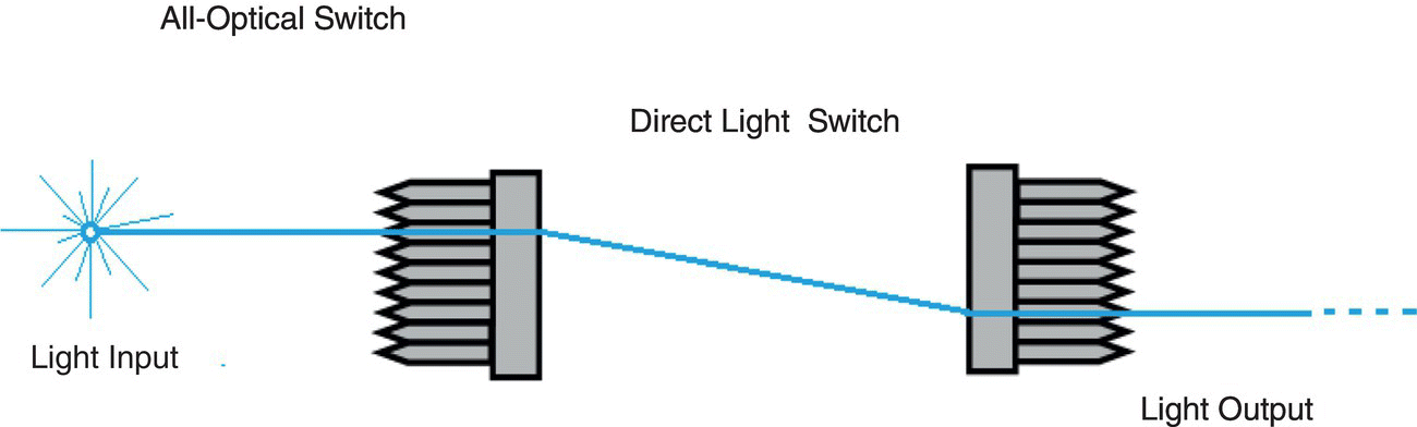
Figure 4.3 All‐optical switch.
- IP packets will not route selectively.
- Optical input, optical switch core, and optical output are used in all‐optical switches.
- OEO (Optical‐Electrical‐Optical) conversion is not used.
- Whole light signal switches from one fiber to another.
- No conversion needed in switching data.
- No data corruption or latency, no timing jitter.
Single‐mode signals with 1260–1675 nm wavelength and multimode signals with 850 and 1300 nm wavelength propagating through all‐optical switches can be transferred and routed. All‐optical switches allow data to transfer at any rate and in any format, no data conversion routing method is required. Video, audio, data, and optical sensor signals can route through all‐optic switches with 400 Gbps+ bandwidth [7]. Conventional copper switches are surpassed by fiber switches.
The static fiber layer is used in optical switches. Patching or manual intervention is not needed in optic switch as cabling needs to be done only once and can be reconfigured remotely. Optical switches create transparent paths with near zero latency, which reduces cost, power usage, and electrical conversion delays. Fiber‐optic switching uses management software in addition to maintain an inventory of cross‐connects routing.
There are three types of all‐optical switches
In the first example (Figure 4.4), the switch is shown on the right. The object here, a single light beam (white), is now released from indirect material in addition to the exit routes. The item here is currently in one of the two switching regions; the “off” state. The current switch turns “on” side, when a second light (black), is imposed onto a nonlinear optical switch and the output beam now changes its direction.
The second example (Figure 4.5) is where one beam of light (white) passes through an indirect device in addition to the exit in a certain direction. The item is in “on” mode. The “off” state of the beam is now reached when the current weak (black) light is injected into the indirect glass device, which will change the direction of the white light.
In the third example (Figure 4.6), a single beam of light (white) passes through an indirect device in addition to the exit in a certain direction. The item here is in one of the two switching regions: the current switch turns to the “off” state when the second light beam (black), is now injected into the indirect material [8]. For this reason, the light of both the first light (white) in addition to the circuit light (black) is present and absorbs the material; in addition, there is currently no output light for either.

Figure 4.4 All‐optical switch that changes the direction of output light.

Figure 4.5 All‐optical switch that redirects light.
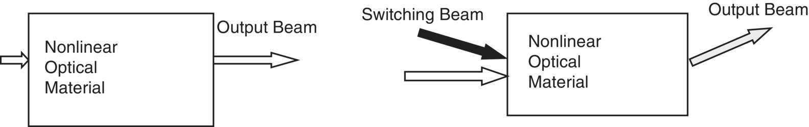
Figure 4.6 Absorptive all‐optical switch
4.2.1 Why is an All‐Optical Switch Useful?
Electronic models were used in the same way as existing electronic devices. The most important power supply at the moment is two opposite wires so the current can be disconnected or added to the communication – “Off” or “On” respectively. In an electric switch, electricity is used for the on/off operation. An all‐optical switch performs the same operation using light.
Undoubtedly, all‐electrical switches are very useful at the moment. At present there is a large presence capable of switching off the “on” power supply in addition to “turning off” the power supply in addition to the use of a switch to control the signal stream in the network. Interestingly, even more important at the moment is the use of all‐electric power that is enjoyed as a transistor usage for digital smart circuits. The concept is now available in both variables (“on” plus “off”) and all electronics because the current switching condition is controlled by other electronic signals.
All‐optical switches are capable of carrying out the same functions as those of all‐electronic switches, for example, directing the streams signal around optical networks or serving as the building blocks of optical computers.
An area connected to all‐optical switches that are now essential for communication exists, taking into account the fact that these days most long‐distance phones are added to the existing internet communications carried by optical cables. These thin sections of glass allow a lot of information to travel long distances near the speed of light. Although we all currently use a lot of optical cables, the computer data available is not an optical signal. Wherever the data signal is switched by wires to reach their destination, the signal must be switched on and converted to electricity so that the current address is able to be read in addition to the data now capable of existing pointing in the right direction. The task of replacing the signal from light to electricity as well as back again uses more power (and causes more heat) and products currently in place will be able to judge whether there is a transfer to occur immediately or several times in a row [6]. The effectiveness of optical communication is increased if the devices are now designed to guide signals while they are currently in optical mode.
All‐optical computing is still the technology of the future. It has some important advantages compared to electronic computers, such as the small size/high density, high speed, and low heating of the joints and the substrate. However, we are very interested in the possibility of using an improved model as our all‐optical switch is an alternative for computing and communication‐based. An all‐optical switch alternative for effective computing and communication should have the ability to identify or deal with single photons.
In the air or in vacuum, the light beams move easily and without interruption. Therefore, in the case of light, it is not possible to change the path of the same light. On the other hand, in a nonlinear material, a strong enough light beam changes the optical properties of material, which can affect any light beam also propagating through the material. Therefore, one beam on the material can control the interaction of the material and another beam. Therefore, one beam can cause a second beam to change direction.
The problem is, this kind of light‐to‐light control happens; the lights and material should interact continuously. Materials usually react as needed only when there are strong light sources. This means that a high‐power beam requires monitoring for even small light by light interactions. These high forces reduce the production design for all‐optical devices as more advanced measures are needed, which increases the cost. Therefore, the difficulty is in finding the right light‐matter interaction necessary to make all‐optical switches.
In order to create a useful all‐optical switch, one has to adjust the operating conditions of the light. Several mechanisms are in place to increase the intensity of light interactions. Research includes the use of light whose frequency is proportional to the amount of light emitted by an atom when the electron is resting from a excited state to a ground state. This technique is called the “resonant enhancement” of light interactions, which simply means that by illuminating the same light source on the atom it emits, the light and the atom interact more easily than if another lights were used.
A nonlinear material formed by a different type of atom can have a strong interaction of light‐matter due to the resonant enhancement [1]; for example, the use of a material that includes only rubidium atoms allows it to have the strong light‐to‐light interactions required for all‐optical switching. On the other hand, most modern television devices are made from semiconductor materials, where resonant enhancement does not work. Therefore, further research is needed to find ways to apply the principles that allow for all‐optical switching in our current devices and available technology.
Increased performance lights up the wavelength in small electrical currents. The effect of each individual increase on the previous channels is irrelevant. Therefore, balance can be maintained. The downside is the length of time required for the connection to be made and for increasing the complexity to the full design.
The concept of multicast packet‐oriented networks has been widely studied in the past due to the increasing number of additional bandwidth‐powered applications [7]. By adding that focus to optical domains, packet‐based applications such as broadband video, high‐definition TV, storage space and network, and multimedia can be provided with additional functionality. In addition, other benefits such as improved performance can occur. This has led to interest in the latest developments in optical multicast networks.
Change operation speed is also important. New wavelength lighting should be done quickly or slowly and with increasing speed performance that allows the optical path to stabilize before the protection mechanism is triggered. They need to stabilize the time in the sub‐millisecond range, which may not be possible with all‐optical components. The effect of each individual increase on the previously associated steps is irrelevant. Therefore, calming down with time can be a relief. The disadvantage is the length of time required for the connection to be made and for increasing the complexity to the full structure. Various tests use optical switches. Time‐consuming tests such as polarization‐dependent‐loss or insertion‐loss measurements are performed on a multiport optical system, and we find significant time savings when manufacturing done by fast, reliable optical switches to turn between the systems port and test equipment. The evolution of the switch in a multifunctional all‐optical device has enabled many novel styles that may not have been available before. These applications originate from user networks such as dynamic all‐optical networks and optical burst switching to test equipment and delay lines.
4.3 Magneto‐Optical Switches
Magnetic‐optical switches use Faraday magneto‐optical switching. Capable of changing the external magnet, this type of magnetic‐optical switch uses Faraday rotation to change the polarization plane of the event that controls the lights to change the optical modes. Compared to the traditional optical switch, the magneto‐optical switch has the advantages of a high‐speed switch and strong stability. Compared to other non‐electronic optical switches, it also handles low voltage better and has low crosstalk. Naturally, it is now slowly gaining widespread use in fiber networks.
4.3.1 Magneto‐Optical Switch Features
- Solid‐state high speed
- High stability, high reliability
- Low driving voltage
- Low cross talk
- Epoxy‐free on optical path
- Fail‐safe latching
- Built‐in circulator and isolator functions
Magnetic‐optical switches are widely used in the running of any optical network. They generally consist of a PBS (polarization beam splitter), FR (Faraday rotator), separator lamp removing polarization, and polarization beam connector [5]. During the usage of a magnetic‐optical switch, the lamp is first divided into orthogonal polarization PBS, and then the magneto‐optical switch will change the polarization plane of this phenomenon, polarize the lamp, and change the external magnet to finally determine the function of the switch
Fiber‐optic beam splitters are used to separate light from one fiber to other fibers. The light from the insertion fiber is first collected, then sent through a fiber‐optic splitter to split it in two. The result of the output beams will be traced back into the output fiber. Both 1XN and 2XN splitters can be built in this fashion, with as many as eight or more outputs with both low return loss and minimal insertion loss. This design is highly flexible, allowing one to use different types of fibers at different channels, and different ports and different beam splitter optics inside. The custom design includes circulators, polarizing splitters, and non‐polarizing plates in one commonly manufactured package. Splitters are made up either of fiber that is completely attached to each port (pigtail system) or of equipment at each station where one can inject the fiber inside (reception method).
The common types of splitters offered are polarizing beam splitters and polarization to protect beam splitters. The operating modes are described below.
In polarization conservation splitters, plates use a reflective mirror to transfer part of the light from the insertion fiber to the main output fiber, and to show the remaining light to the second output fiber. Separated polarization uses a well‐designed multi‐parting light with the exact ratio regardless of the incoming polarization. Due to the nature of this coating, the performance will vary in length, and therefore it is recommended for a working wavelength range of about ±10 nm. Broadband beam splitters are supplied, but with significant variation of the split component they have to do with setting polarization. Splitters that only divide a small part of the input light are commonly known as taps. These splitters are commonly used in power tests. There is a very low‐cost alternative solution, including tap operation and photodiode testing in one unit.

Figure 4.7 Polarization orientation on polarizing fiber beam splitters.
In split beam splitters, polarizing beam splitters divide incoming lights into two orthogonal states. They can also be used to combine light from two fibers to form a single output fiber. When used as a connecting beam, each input signal transmits on a different output polarization axis. It is important when using these splitters with polarization to preserve the fiber that one understands how polarization axes fit on each channel. Figure 4.7 one shows the standard configuration. With this configuration, the following behavior will be observed.
- The slow axis of T input port induces light to slow axis of output port 1.
- The fast axis of T input port induces light to slow axis of output port 2.
- The slow axis of R input port induces light to fast axis of output port 1.
- The fast axis of R input port induces light to fast axis of output port 2.
This configuration may change as per customer need.
In the polarizing splitters there are two factors to consider: the ability of the splitter to prevent the light arranged at port 1 to reach port 2 and to maintain the polarization extension of light emerging fibers at each port. The level of crosstalk is equal to or greater than that of the split extinction level. For example, splitter can be made with the high crosstalk ratio, but if the output fibers have has a medium shape, then the output polarization extension ratio intend be lower.
4.3.2 Principles of Magneto‐Optical Switches
Compared to the traditional mechanical‐optical switch, the magneto‐optical switch [9] has the advantages of being a high‐speed switch and having strong stability. Compared to other non‐electronic optical switches, the magneto‐optical switch has the advantages of lower driving voltage and smaller crosstalk. In the near future, the magneto‐optical switch aims to be a competitive product.
4.3.2.1 The Design Core of the Magneto‐Optical Switch
The Faraday rotation effect was applied to the magneto‐optical switch. Adjust the action of the magnetic‐optic crystals in the event of lighting and a polarized plane by adding the external magnet, to gain the ability to change the optical path. In other words, the Faraday rotation effect is the event that the separation plane rotates when linearly polarized light passes through the center in an external magnetic field. There is a polarized lamp with a line next to M in the center, which can be divided into two circular lights on the other side. And then the two circular flashing lights scatter forward in two different velocities without any interaction. After illumination, there is only a step difference between them. Therefore, the light output is still refined, but the separation plane rotates in a certain direction compared to the light‐paced event. This means that when the outer magnet acts on the magneto‐optical crystal, its separation state can be changed after the illumination of the light.
The magneto‐optical switch can detect the e‐optical switching function that is required for all‐optical communication.
4.3.3 Magneto‐Optic Effect
Magnetic‐optic effect refers to the physical contact between light and magnetism. Once the light source enters the source material, the light emissions can be adjusted by the interaction of the light‐object, such as the polarization, spectrum, phase, and intensity of light. The magneto‐optic system [9] has played important roles in the evolutionary history of electrical engineering, as it provides a solid basis for experimenting to understand electromagnetic theory, classical theory of matter, and quantum theory. In 1845, Michael Faraday observed that when a light passed through a glass toward the outer magnet, its polarization angle was rotated by angle. This is the first time that the magnetic‐optic performance (Faraday effect) was tested and provides some solid evidence that light is an electromagnetic wave in nature [10]. In 1876, John Kerr observed a plane of light reflected from a magnetic field. Demonstrating such a magneto‐optic effect will be called the magneto‐optic Kerr effect (MOKE). The sensitivity of MOKE is very high as it can be affected by sub‐atomic layer magnetism, so this is an ideal tool for reflecting magnetic ground‐side systems, especially for atomic‐thickness two‐dimensional (2D) materials and other nanostructures. Subsequently, the Zeeman endings and the magneto‐birefringence endings (Voigt effect and Cotton–Mouton effect respectively) were obtained. Currently, giant magnetic‐optic effects have been found in many magnetic objects, such as rare‐ground element‐doped garnets, rare‐ground element‐doped magneto‐optical glasses, rare‐ground element‐doped iron garnet films and magnetic alloy films. Due to its high sensitivity, low power output or even no power supply (if magnets are constantly used) and high‐efficiency, magneto‐optic results are attracting great interest from scientists and engineers in different fields. In particular, as the future of electronics grows to focus on the atomic level, conventional devices, or technologies for magnetic resonance imaging, such as vibrating magnetometer sampling and superconducting quantum interference technology (SQUID), may lose performance. Therefore, it is essential to use the MOKE or Zeeman results as high‐throughput systems for analyzing the physical properties of micro, nano, or even systemic systems, as they show a meaningful retaliation to the magnetism of the subatomic layer. Meantime, improvements to compact and sensitive magnetic‐optic systems are also promising the realization of future lighting modulation with the advantages of non‐interference, low power consumption, and non‐damage.
The Cotton–Mouton effect refers to the behavior of 2D materials diffused in liquid. The other three effects are characterized in the form of solids. The 2D material shown is in xy‐plane. In contrast, 2D products are a class of sheet‐type non‐standard, with a thickness of hundreds of nanometer or sub‐nanometer. Depending on the specified measurement ? = l/t, where l and t are the back size and thickness, 2D materials have a very large form anisotropy r. Since the discovery of graphene in 2004, it has been found that the 2D substance family has more than 1000 elements, such as iron dichalcogenides (TMDCs), black phosphorus (BP), hexagonal boron nitride (h‐BN), and iron oxides. In general, most of the objects are designed with a strong intra‐buffer connection while weak van der Waals forces between the components, enabling the surface preparation of 2D object from multiple suspensions and extensions. Meanwhile, chemical carbon deposition (CVD) is widely used to create high‐quality 2D crystals. Currently, bands of 2D products cover a wide range, and that family of 2D products contains protective, semiconducting, and metallic materials. Again, by creating separate 2D elements on top of each other, the new and magnetic properties of 2D heterostructures can be enhanced. Thus, the magneto‐optic output of 2D objects has become one of the areas of research in recent years, as it reflects a wide range of physical phenomena. Figure 4.8 shows the fourth case‐based analysis of magneto‐optic effects of 2D objects, related to the interaction between light event and 2D objects in front of an external magnetic field. In 2011, the giant Faraday effect of graphene was reported. More recently, due to its increased Dirac electron dispersion and chiral characteristics of the electromagnetic field, graphene was found to contain half‐dimensional Hall effect, which results in a higher Faraday effect and MOKE. Even with 2D magnetic field devices, such as TMDCs, the large Zeeman effects determined by the magnet field caused a clear valley crack of 3030 μeV/T observed. The reported 2D giant magneto‐optic devices work with the latest magnetic 2D objects, such as Cr2Ge2Te6, Fe3GeTe2, and CrI3, as well as opening up new 2D objects based on magneto‐optic writing and also laying the groundwork for further deep‐diving on the search for open source magneto‐optic effects.
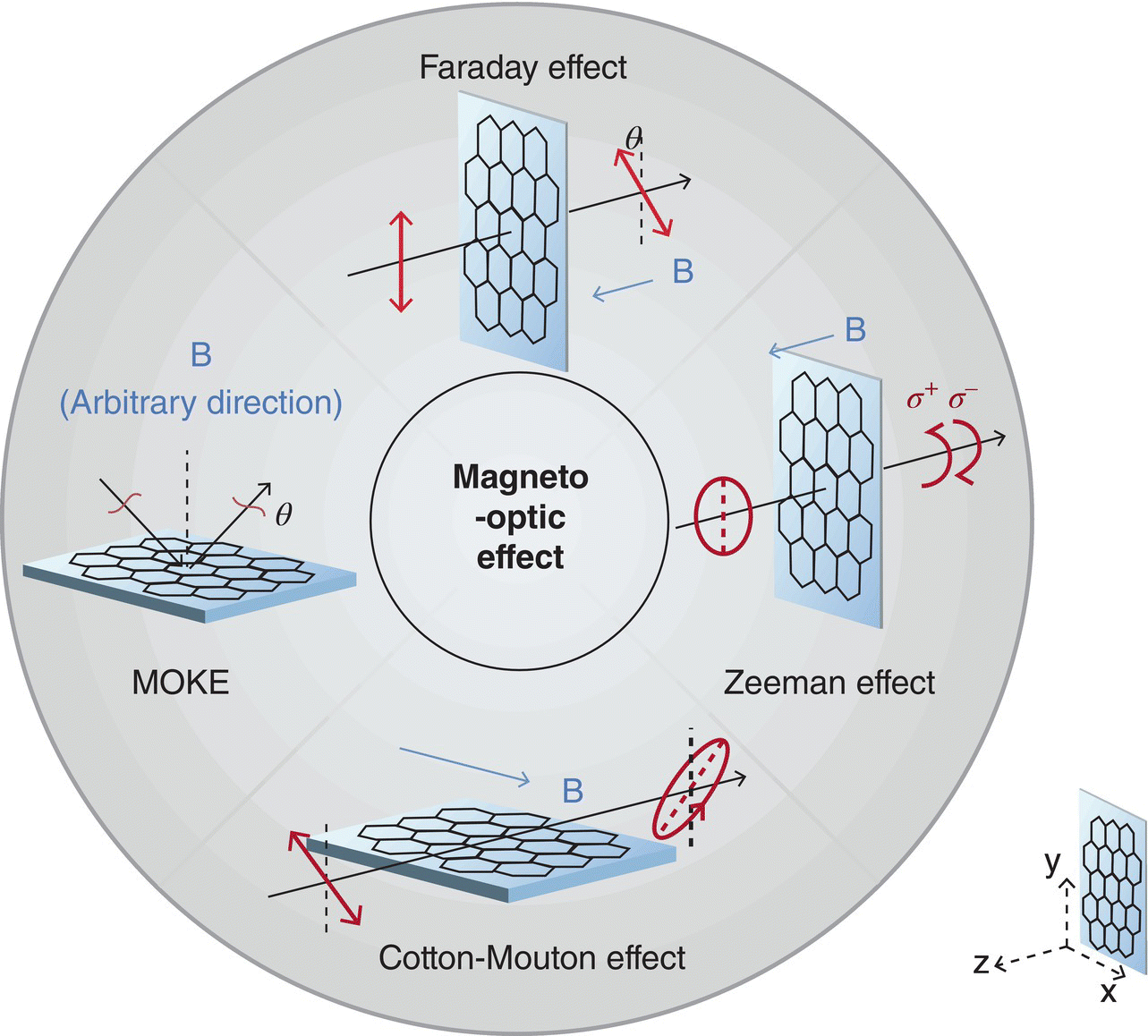
Figure 4.8 Typical magneto‐optic effects of two‐dimensional (2D) materials: Faraday effect, magneto‐optic Kerr effect (MOKE), Cotton–Mouton effect, and Zeeman effect.
4.4 Faraday Rotation
The inception of Faraday rotation was explained by two possible models – the phenomenological model and the atomic model – by Balanis and Zvezdin respectively [9, 10].
4.4.1 Phenomenological Model
In this model magnetic field objects are replaced by a description of magnetic dipoles corresponding to each other creating the magnetic state of the object. When the outer field is used the dipoles are rotated by a field path. It is similar to the direction of the top of the magnetic field in a magnetic field, a fixed magnetic field that rotates with a constant frequency, known as the Larmor precession frequency, in front of the external magnetic field. As the way that torque exerted is by the gravitational field on a spinning top, single magnetic dipole moment m exerted by an external magnetic field exerts a torque T given as
Where m= nIds, H0 is the applied magnetic field and B0 is the applied magnetic flux density.
4.4.2 Atomic Model
The atomic model describes magneto‐optic (MO) features, so free‐ion theory is useful in explaining the magneto‐optical effects of quantum mechanics [4]. The Hamiltonian of a free ion can be written as
H0 is the sum of the one‐half Hamiltonians with the force corresponding to the equal‐center‐field projection, Hee is the energy associated with the magnetic field and Hso is the Hamiltonian defining spin‐orbit interaction. The state of the ion is determined by the distribution of electrons between single electrons, which is also determined by the Paul–Fermi principle and by the low power of the ion. Most of the magnetic‐optical properties are controlled by ions touching incomplete 3d and 4f shells. For these Russel–Saunders coupling (LS coupling) means spin‐spin and orbit‐orbit coupling is the strongest. Here the orbital angular time of the electric field is so strong that it communicates with a different full L and/or different full S with a different power. Thus the ground configuration, defined by H0, is divided into characteristics of the (Spin) S and (orbital) L time, and the state is defined by the waves of activity (k; S, L, Ms, ML), where K is the configuration index.
If there is any solid or liquid is applied to the magnetic field of the field, and the field beam is polarized and passed through it in the direction of the magnetic lines of force (through holes in the pole of the electric field gate), they found that the transmitted light is still a fixed plane. This “optical rotation” is called the Faraday rotation (or Faraday effect) and contradicts significant aspects of a similar effect, called the optical phenomenon, occurring in a sugar solution [6]. In a sugar solution, the circular motion goes the same way, whichever way the light beam is directed. In Faraday practice, however, the optical rotation, such as when looking inside a band, is restored when the light exceeds an object facing the magnetic field; that is, the rotation can be restored by changing the field direction or the direction of light. By setting an example between two pieces of Polaroid or two Nicol prisms, it can be arranged (with sufficient magnetic force) so that small light is passed through the system in one way, while it can pass, eventually without exhaustion, in opposite directions. The result is that it allows the construction of an irreplaceable mirror object such that observer A can see observer B, while A cannot be detected by B.

Figure 4.9 Polarization rotation due to the Faraday effect.
Magneto‐optic results are cases in which the optical properties of an object are altered by the presence of a quasi‐static magnetic field (either externally applied, or due to the magnetization of that object). The first discovery of a magnetic‐optical effect, now known as the Faraday effect, occurs when a light separated differs when passing through an object exposed to a magnetic field directly aligned to the light direction. Under these conditions, the polarization of plane appears to rotate; this cycle is called the Faraday rotation (Figure 4.9).
The strength of the polarization rotation due to the Faraday effect is defined according to the empirical relationship:
Here, V is the Verdet constant of the material, D the thickness of the sample, and B is the strength of the magnetic field. For most transparent materials, V is extremely small and is both temperature‐ and wavelength‐dependent.
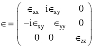
The permitting tensor is the traditional first point of access for the Faraday Output (although the magneto‐optic output can be the equivalent taken from the load tensor). To explain the Faraday effect, dielectric permittivity is treated as a non‐diagonal tensor taking form (for propagation in the z direction). Here, the specification of the applied magnet (or magnetization) is taken as an axis. The diagonal properties represent the operation of objects in the absence of magnetic‐optic results. The diagonal element ϵxx is the origin of the Faraday effect: it can be shown that non‐zero ϵxx creates a phase lag between left‐right and right‐handed circularly polarized components of linearly polarized light, which results in rotation of the polarization plane.
One of the unique and important features of Faraday rotation is its non‐reciprocal character; if the light makes two opposite faces passing through magnetic‐optic objects, the Faraday rotation does not cancel (such as the polarization rotation due to the optical event) but rather doubles. This non‐repetition allows the Faraday effect to be used as a operating principle for optical isolator and optical circulators, important components in optical telecommunications and other laser applications.
Bibliography
- 1 D. Papadimitriou et al. Optical multicast – a framework. OIF2001.093, April 2001.
- 2 Karl Heinz Bennemann. Non‐Linear Optics in Metals. No. 98. Oxford, Oxford University Press, 1998.
- 3 R. Doverspike and J. Yates. Challenges for MPLS in optical network restoration. IEEE Communications, February 2001.
- 4 B. Mukherjee et al. Light trees: optical multicasting for improved performance in wavelength router networks, IEEE Communications Magazine, February 1999.
- 5 C. Leycuras, H. Le Gall, J. Desvignes, M. Guillot, and A. Marchand. Magnetic and magneto‐optical properties of a cerium YIG single crystal. IEEE Transactions on Magnetics, 21(5): 1660–1662, 1984.
- 6 N. Ghani, J. Fu, D. Guo, X. Liu, Z. Zhang, P. Bonenfant, L. Zhang, A. Rodriguez Moral, M. Krishnaswamy, D. Papadimitriou, S. Dharanikota, and R. Jain. Architectural framework for automatic protection provisioning in dynamic optical rings. OIF 2001.041, January 2001.
- 7 D. Papadimitriou. Optical rings and optical hybrid mesh‐rings topologies, Internet draft, work in progress, https://datatracker.ietf.org/doc/html/draft‐papadimitriou‐optical‐rings‐00, February 2001.
- 8 S. Ayandeh and P. Veitch. Dynamic protection and restoration in multilayer networks. OIF 2001.166, April 2001.
- 9 A.K. Zvezdin and Y.A. Kotov. Modern Magnetooptics and Magnetooptical Materials. Bristol, Institute of Physics Publishing, 1997.
- 10 C.A. Balanis. Advanced Engineering Electromagnetics, Chichester, John Wiley and Sons, 1989.
Further Reading
- E.U. Condon and G.H. Shortley. Theory of Atomic Spectra. Cambridge, Cambridge University Press, 1959.
- A. Cotton and H. Mouton. Influence of polydispersity on the phase behavior of colloidal goethite. Annales de chimie et de physique, 11:145, 1907.
- M. Faraday. Experimental researches in electricity. Nineteenth Series. Philosophical Transactions of the Royal Society London, 136:1, 1846.
- T. Hayakawa and M. Nogami. Dynamical Faraday rotation effects of sol–gel derived Al2O3–SiO2 glass containing Eu2+ ions. Solid State Communications, 116:77, 2000.
- T. Hayakawa, M. Nogami, N. Nishi, and N. Sawanobori. Faraday rotation effect of highly Tb2O3/Dy2O3‐Concentrated B2O3−Ga2O3−SiO2−P2O5 glasses. Chemistry of Materials, 14:3223, 2002.
- T. Kato, S. Iwata, M. Yasui, K. Fukawa, and S. Tsunashima. Magneto‐optical spectra of (Mn1‐xMx)Pt3 (M‐Fe, Co) ordered alloy films. Journal of Magnetism and Magnetic Materials, 177–181:1427, 1998.
- J. Kerr. XLIII. On rotation of the plane of polarization by reflection from the pole of a magnet. Philosophical Magazine Series 1, 3:321, 1877.
- J. Kerr. JXXIV. On reflection of polarized light from the equatorial surface of a magnet. Philosophical Magazine Series 1, 5:161, 1878.
- M. Kucera, J. Bok, and K. Nitsch. Faraday rotation and MCD in Ce doped yig. Solid State Communications, 69:1117, 1989.
- C. Leycuras, H. Le Gall, J.M. Desvignes, M. Guillot, and A. Marchand. Magneto‐optic and magnetic properties of praseodymium substituted garnets. Journal of Applied Physics, 53(11):7125–8425, 1982.
- W. Liu, Y.H. Dai, Y.E. Yang, J.Y. Fan, L. Pi, L. Zhang, and Y.H. Zhang. Critical behavior of the single‐crystalline van der Waals bonded ferromagnet Cr2Ge2Te6. Physical Review B, 98, 214420, 2018.
- K. Nassau. Handbook of Laser Science and Technology, Supplement 2: Optical Materials. Boca Raton, FL, CRC Press, 1995.
- S. Novoselov, A.K. Geim, S.V. Morozov, D. Jiang, Y. Zhang, S.V. Dubonos, I.V. Grigorieva, and A.A. Firsov. Electric field effect in atomically thin carbon films. Science, 306:666, 2004.
- M. Shamonin, T. Beuker, P. Rosen, M. Klank, O. Hagedorn, and H. Dotsch. Feasibility of magneto‐optic flaw visualization using thin garnet films. NDT and E International, 33:547, 2000.
- A. Vafafard and M. Sahrai. Tunable optical and magneto‐optical Faraday and Kerr rotations in a dielectric slab doped with double‐V type atoms. Scientific Reports, 10:8544, 2020.
- W. Voigt. Doppelbrechung von im Magnetfelde befindlichem Natriumdampf in der Rischtung normal zu den Kraftlinien. Mathematisch‐Physikalische Klasse, 1898:355, 1898.
- Q.H. Wang, K. Kalantarzadeh, A. Kis, J.N. Coleman, and M.S. Strano. Electronics and optoelectronics of two‐dimensional transition metal dichalcogenides. Nature Nanotechnology, 7:699, 2012.
- Y. Xu, J.H. Yang, and X.J. Zhang. Quantum theory of the strong magneto‐optical effect of Ce‐substituted yttrium iron garnet. Physical Review B, 50:13428, 1994.
- P. Zeeman. On the influence of magnetism on the nature of light emitted by a substance. Astrophysical Journal 5:332, 1897.
- X. Zhang, Z. Lai, C. Tan, and H. Zhang. Solution‐processed two‐dimensional MoS2 nanosheets: preparation, hybridization, and applications. Angewandte Chemie, 55:8816, 2016.