
The MCS51 Microcontroller
The 8051, like many microcontrollers, has the CPU, memory and I/O (Input/Output) integrated together in a flexible and extendable manner. It is an established product which is very popular in many different industries. The core features of the device are
• 8-bit CPU optimized for control applications
• Extensive Boolean processing (single-bit logic) capabilities
• 64K Program Memory address space
• 64K Data Memory address space
• 4K bytes of on-chip Program Memory
• 128 bytes of on-chip Data RAM
• 32 bidirectional and individually addressable I/O lines
• 6-source/5-vector interrupt structure with two priority levels
The basic architectural structure of the core is shown in Figure 2.1.

Family Members/Variants
The MCS51 microcontroller family comes in a variety of options, and a selection of these are summarized in Table 2.1.
Table 2.1

Basically, the options available from the MCS51 family are:
• A microcontroller with internal mask-programmed ROM
This is the option chosen for mass-produced items. The act of specifying and creating a mask-programmed ROM is an expensive capital outlay, but the unit cost falls to a very low level if the economies of scale determine that enough devices can be ordered.
• A microcontroller with internal EPROM
This option is chosen for prototyping/developing microcontroller software, or for short production runs. The EPROM-based 8751 is relatively expensive and has the limitation that it will only tolerate 100 erase/program cycles (manufacturer’s figures). Against this high(ish) initial outlay, it must be remembered that these devices hold software. The cost of developing software is the most significant part of any project.
Both the ROM- and EPROM-based versions have an inbuilt ‘security fuse’. This controls the memory read mechanism, so that an external device cannot read the ROM (i.e. ‘steal’ the software).
• A microcontroller with external program memory
This is the cheapest option. The drawback is that some of the I/O pins now have to be used for accessing the external memory device(s). This is acceptable if the device additionally has to access other peripheral or memory components. It is also a less expensive development method since EPROM programmers are cheaper than 8751 programmers. The exact interface circuitry is detailed on page 19. The cost of the 8031 is of the same order as the basic PIC model; however, memory and interface still have to be paid for. In Figure 2.2(a), Pins 32–39, 16, 17 and several of 21–28 (depending on memory size) would be needed for external memory devices.

The DS750 family is a reaction to consumer demand for a physically smaller device (0.3 inch pin pitch) with all functions integrated onto the IC. These small (24-pin DIL) microcontrollers come in EPROM or OTPROM program memory. They are not designed for external memory expansion, so are made smaller and more compact. Many engineers feel that this simplification has been achieved at the expense of one major flaw – the serial port is not available in this package. Otherwise, it is generally held to be a good thing.
The 40-pin DIL version shown in Figure 2.2a is the simplest version – i.e. an 8051/8751 (EP)ROM version with all four (8-bit) ports being used as I/O lines. Active-Low lines are identified with a preceding oblique, e.g. /EA.
(‘Active-Low’ means that a logic 0 is needed for the input to perform its stated function. In this case /EA is pronounced ‘not-External-Access’ or ‘not-E-A’. The implication is that in order to access external memory, this line should be tied low to 0 V.)
Common to all electronic circuits are the power supply lines VCC and VSS. In some variants, these may be called VDD (= VCC) or GND (= VSS). Technically, this is a mix of terminology since VCC is usually used for +V bipolar transistor supplies and VSS is usually used for MOS Ground supplies. However, it is the terminology used by Intel. The letter ‘C’ in the designation implies a CMOS (low power variant). The power supplies needed are:
| Voltage | Current |
| VCC= +5 | 160 mA/20mA (8031/80C31) or |
| VSS = 0V | 250 mA/40 mA (8751/87C51) |
The following section will cover the housekeeping input lines RST, XTAL1, XTAL2 and Vpp|/EA. (/PROG|ALE and /PSEN are outputs and will be explained later.)
Reset
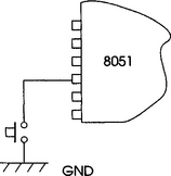
RST is the system ReSeT line. It is essential to reset the microcontroller at power-up to initialize internal control registers. RST is an active high control line which will reset the microcontroller when a logic ‘1’ is applied to it. The circuit of Figure 2.3 shows the basic configuration, with a switch added as an option to provide manual (additional) reset if required. The R-C circuit provides a time delay which must hold the RST line HIGH for a minimum of 24 oscillator periods.

The Watchdog Timer
In some designs it is considered necessary to add a WATCHDOG controller. This is a separate integrated circuit which will reset the microprocessor automatically if it is not regularly ‘serviced’ (send a logic signal from the microcontroller to reset the watchdog). It also provides the power-on-reset function of Figure 2.3. It is difficult to guarantee the integrity of any software, so if an error occurs, such as the microcontroller hanging up while waiting for an input which never arrives or getting stuck in a software loop, then the watchdog would not be serviced, so it would generate a reset.
Figure 2.4 shows one type of watchdog controller that integrates the reset function. Some members of the 8051 family have an inbuilt watchdog that can be programmed into the users’ designs if necessary. These include the ’542, ’550, ’552, ’558, ’562, ’580 and ’592 variants.

Clock and Resonator Circuits
All microprocessors require a clock. It is used to synchronize all the activities and data transfers within the CPU. Originally, the 8051 used quartz crystals up to 12 MHz, but later designs are capable of operating at up to 40 MHz. Figure 2.5(a) shows a circuit suitable for a 12 MHz crystal. This sounds quite a fast rate (40 MHz has period of some 25 ns) but the Intel family of devices divide this rate by 12 internally to produce the machine cycle – the basic interval which handles single-byte instructions. This brings the machine cycle rate down to 1 MHz (or up to 3.33 MHz for a 40 MHz clock).

If low cost or minimum component count is of prime importance, then consider the use of 3-terminal ceramic resonators which are made from barium titanate. These small devices have a central pin which is connected to ground. No capacitors are required. The disadvantages are:
• not as accurate as crystals (0.5% as compared to 0.002%)
• not as stable as crystals (as compared to 0.005%)
• not available in as high a frequency range as crystals (only up to 8 MHz).
Figure 2.5(b) shows a typical connection.

Figure 2.5(b)
VPP|/EA is a control pin which has two functions. VPP is a programming voltage for the EPROM version. A high voltage (12.5 V or 21 V, dependent on version) is used to store the users’ programs on the internal EPROM. An 8751 programmer will apply address and data signals to the device, and a controlled pulse applied to the ALE pin will use the high voltage on the VPP pin to store the data.
/EA is a signal which informs the MCS51 to look for its program in External Memory. If /EA is high (+5 V), the device looks for its program in internal EPROM. If /EA is low (0 V) the device looks for its program in external EPROM. Several examples of applications of /EA will be given in the memory decoding section.
I/O Port Structures
All four ports in the MCS51 family are bidirectional. Each consists of a latch, an output driver, and an input buffer. When using the 8051/8751, all four ports can be used as inputs or outputs. Each I/O line can be independently used as an input or an output (although as an output, the pins can sink more than they can source). A source output is when current is output from the microprocessor (the microprocessor ‘sources’ current). A sink output is when current enters the output port (the microprocessor acts as a current ‘sink’). Figure 2.6 shows the difference.

Ports 1, 2 and 3 are called quasi-bidirectional. After the 8051 has been powered up or after a RESET, all ports act as inputs. The exception to this is when the EA (External Access) pin is connected to 0 V in order to instruct the IC to access external program memory. In this case, Ports 0 and 2 have special functions which I will deal with shortly. The quasi-bidirectional structures are shown in Figure 2.7. Ports 1 and 3 (and Port 2 if not used to access memory) have a ‘weak internal pull up’ formed from a FET switch. When used as an output, each pin of each of these ports will turn on the lower FET to output a ‘0’ or it will turn off the lower FET to output a ‘1’ via the pull-up resistor. This is the reason why the 8051 ports can sink more current than they can source. The lower FET represents a low impedance connection to ground when it is turned on, while the pull-up resistor (FET) is a higher impedance. The diagrams are actually a little oversimplified. In parallel with the pull-up ‘resistor’, there is another FET which switches on for 2 oscillator periods whenever a ‘1’ is to be output. This FET pulls the output voltage up sharply, i.e. if there is a capacitive load, it would be rapidly charged to the VCC potential and would stay there once the weak pull-up was the only output device.

This facility is useful, because if you wish to create an input from (say) a push-to-make push-button, then the only circuit needed is that of Figure 2.8. Reading this pin would normally result in a ‘1’ being input since the pull-up resistor would connect that voltage to the CPU buffer. Pressing the button would connect the pin to ground and hence a 0 V would be input.
When using the pin as an output, the only care that must be taken is that you must not write a ‘0’ out on that pin before trying to use it again as an input. To do so would cause a conflict with any devices which may be connected to the pin. If an external device is trying to input a ‘1’ and the 8051 is simultaneously trying to output a ‘0’, then catastrophe will be the only result! The output FET of the 8051 is capable of sinking up to 0.5 mA which could damage sensitive devices which are trying to output a logic ‘1’. Alternatively, if the external device trying to put a signal into the 8051 is capable of outputting more than 15 mA, then there is a good chance of damaging the input buffer of the 8051. In practice, though, it is rare to want to use a port as both input and output, so this situation should not arise.

Port 0 is different. This port has no weak pull-up because of its capability to read from and write to external memory devices. It has two output FETs which provide high current paths to either the +VCC or GND supplies. The pull-up FET only operates when executing an instruction which causes it to access external memory. The output pins for normal operation are ‘open-drain’, i.e. only connected to the lower pull-down FET. It would need external pull-up resistors to function in the same way as Figure 2.7. It is a true bidirectional port because when used as an input, the pins float (are not connected to any particular voltage).
Some Design Examples
Figure 2.10 is a simple example of an 8751 being used as a combinational door lock controller. Port 1 is used to operate a 16-key matrix keypad, while Port 2 operates the indicator lights and door solenoid.

The keypad is arranged in columns and rows. Pressing a key causes a column to be connected to a row. The software of the MCS51 must sequentially ‘strobe’ the four columns. This means that it outputs a logic ‘1’ pulse to column 1; then a logic ‘1’ pulse to column 2 and so on. While a column is driven high by a logic ‘1’, the microprocessor inputs the data on the 4 rows. If a button in that column is pressed, it will be sensed in the appropriate row.
In Chapter 4 (page 113) a dedicated keyboard interface IC is introduced. This is the 74C922. The design in Figure 2.10 uses 8 pins connected to the microcontroller, while the 74C922 would only connect 5 pins to the IC. Chapter 4 (page 113) explains how to use an output driver IC to increase the current available from the microprocessor.
Accessing External Memory
If the /EA line of the microcontroller is LOW, then Port 0 and Port 2 are used to access the program memory. Every time a byte of data is to be fetched from this external memory the following sequence occurs:
1. Port 0 outputs the low byte of the external memory address while Port 2 outputs the high byte of the external memory address.
2. The ALE line (pin 30) is asserted – this will cause the lower byte of the address to be stored by an external latch (see Figure 2.11).

3. Port 0 is ‘floated’ (put in a high impedance mode).
4. /PSEN (pin 29) is asserted. This signal operates the external memory device (i.e. /CE of the EPROM).
This is somewhat confusing as a word description, so Figure 2.12 shows the timing of the control signals. The sequence of these signals (ALE and /PSEN) is started automatically by the action of setting /EA low. Additional circuitry would be needed to use these signals and Figure 2.14 shows how this could be achieved. The latch could be a ’373 or ’573 octal latch. These devices store a byte of data when the E (enable) line is activated.


Logical Separation of Program Memory (read only) and Data Memory (read/write)
An original design feature of the 8051 is that it has separate Program and Data Memory. The microcontroller uses /PSEN (pin 29) to access Program Memory and /RD (pin 17) and /WR (pin 16) to access Data Memory. The logical separation of these two memory spaces allows the Data Memory to be accessed by 8-bit addresses which can be more quickly stored and manipulated by an 8-bit CPU (although 16-bit addresses can be used if necessary).
Figure 2.13 shows the timing of data transfers, while Figure 2.14 shows how the 8031 could support both Program Memory in EPROM and Data Memory in RAM. The distinction is due to the fact that the /PSEN signal is used to access the EPROM, while the /RD – /WR signals are used to access the RAM.

Larger size EPROM and RAM devices can be used directly up to 64 kbytes each. Designers of embedded systems are frequently as interested in target board size as much as cost, so the usual solution is to use as large a memory device as possible, i.e. use 1 × 64 kbyte instead of 4 × 16 kbyte. However, Figure 2.15 shows a fully decoded example with segmented memory and memory-mapped I/O.

A single 16 kbyte memory will have 14 address lines which address
![]()
There are four of these shown in Figure 2.15 and there are a total of 16 address lines of which only 14 are used on each RAM IC. The upper two address lines allow the 74138 to work out which of the RAM IC’s are to be accessed for any particular address. The 74138 is a 3 to 8 line decoder. In this circuit, only two binary inputs are used to determine which of the four chip enable (CE) outputs activate which RAM device.

In this particular example of Figure 2.15, the 8255 I/O port responds to one of four RAM addresses. That is, it appears as if it is 4 of the 64 kbyte memory addresses. To do this, the particular 4 addresses must be detected by the address decoder, and when it enables the 8255 I/O port, it must disable those particular 4 RAM addresses in the RAM devices. The 8255 I/O port has 3 × 8 bit ports A, B and C; so it expands the I/O capability of the microprocessor. The reason it needs 4 discrete addresses is that it has 3 I/O ports and 1 control port. This is an example of ‘memory mapped I/O’ in that the I/O device behaves somewhat like a memory device in that it can be written to and read from.
Non-volatile Memory
There are many situations where it is important not to lose the contents of memory when the power is removed. The two main solutions for this use Electrically Erasable EEPROM or battery/capacitor-backed RAM.
EEPROM is available in serial or parallel access. Serial EEPROM needs special algorithms to save and read data. Parallel EEPROMs are easier to drive since they more closely resemble conventional EPROMs.
RAM whose contents are preserved with backup capacitor or battery are most conveniently interfaced via proprietary control ICs. The difficulty with RAM is that if there is any noise or jitter on the /WE and /CE lines as the main system power shuts down, then parts of memory will be lost. Several manufacturers produce suitable ICs which can be used, as in Figure 2.16. This circuit is also capable of driving the RESET line of the 8031.

Some applications such as data loggers could require much more memory than the 64k directly available from the 8051. Figure 2.17 shows a circuit which uses spare lines of Port 3 to activate different banks of RAM. The 3 to 8 line decoder 74LS138 allows up to 8 × 64 kbytes of memory to be selected. This arrangement could be extended almost indefinitely. In practice, of course, PLDs (Programmable Logic Devices) would be used since they could integrate many other functions.

Port 3 and two lines of Port 1 have alternate functions. These can be used selectively (see Table 2.2).
Table 2.2
| PORT PIN | Alternate Function |
| *P1.0 | T2 (Timer/Counter 2 external input) |
| *P1.1 | T2EX (Timer/Counter 2 Capture/Reload trigger) |
| P3.0 | RXD (serial input port) |
| P3.1 | TXD (serial output port) |
| P3.2 | /INT0 (external interrupt 0) |
| P3.3 | /INT1 (external interrupt 1) |
| P3.4 | T0 (Timer/Counter 0 external input) |
| P3.5 | T1 (Timer/Counter 1 external input) |
| P3.6 | /WR (external data write strobe when/EA is low) |
| P3.7 | /RD (external data read strobe when/EA is low) |
*P1.0 and P1.1 serve these alternate functions only on the 8052 and more complex MCS family parts which have more than just the two timers.
Intel use the dot notation of the form P3.4 to indicate bit 4 of Port 3.
Questions
1. Design the hardware of an 80C51 based electronic die where the input is a single ‘throw’ switch and the output is the drive to a seven-LED array. How could this be reduced to 4 outputs?
2. Show how to interface an 8031 to a 27128 EPROM, a 62128 Static RAM and 2 × 8255 parallel input output interface devices. The 8255 devices should use addresses FF00H–FF03H and FF04H–FF07H.
3. Look forward to page 126; the ADC 0803 analogue to digital converter. Show how to design this into the 8031 based system of question 2 so that the address of the ADC is F000H.
Architecture
We cannot make much more forward progress with the device until more is revealed about the internal architecture of the 8051. Figure 2.1 shows a typical implementation with the four ports, two timers, internal registers and all the other bits and pieces which make up the microcontroller. The base model has 128 bytes of available RAM addressed from 00 to 7F. There is an additional area of RAM from 80 to FF called the Special Function Register (SFR) space which hold registers which control or report on the many functions built into the IC. These two memory areas are called the direct memory space. All of these addresses can be read or written to, but obviously the SFR space is reserved for the special functions. Not all of the 127 locations in SFR are used.
Register Structures
There are 8 general purpose registers which are called R0, R1, R2, R3, R4, R5, R6 and R7. They are not physical registers in the CPU as such. They actually occupy general-purpose RAM addresses 00–07. The 8051 allows the programmer to have 4 sets of these 8 registers. These are called Register Banks 0, 1, 2 and 3, but at any one time there are only 8 active registers called R0–R7. At power-up, the machine defaults to Register Bank 0.
Table 2.3
| Register Bank | Address in RAM of R0–R7 |
| 0 | 00–07 |
| 1 | 08–0F |
| 2 | 10–17 |
| 3 | 18–1F |
So, if Register Bank 0 is selected, storing a number in Register R3 would cause it to be saved at internal RAM location 03. But if Register Bank 1 is selected, storing a number in Register R3 would cause it to be saved at internal RAM location 0B. Obviously, there is a potential problem here which could be caused by moving data from a Register when the wrong Register Bank is selected. The wrong data would be moved. This is the responsibility of the programmer. (The addresses and data shown are in the hexadecimal (16) number base. For an explanation of this, see Appendix B.)
As far as the Special Function Register (SFR) is concerned, Table 2.4 shows the various functions of the Direct Bytes.
Table 2.4
| Direct Byte Address | Hardware Register Symbol | Function |
| F8H | ||
| F0H | B | B Register |
| E8H | ||
| E0H | A or ACC | A Register |
| D8H | ||
| D0H | PSW | Program Status Word |
| C8H | ||
| C0H | ||
| B8H | IP | Interrupt Priority |
| B0H | P3 | Port 3 |
| A8H | IE | Interrupt Enable |
| A0H | P2 | Port 2 |
| 99H | SBUF | Serial Data Buffer |
| 98H | SCON | Serial Control |
| 90H | P1 | Port 1 |
| 8DH | TH1 | Timer 1 High Byte |
| 8CH | TH0 | Timer 0 High Byte |
| 8BH | TL1 | Timer 1 Low Byte |
| 8AH | TL0 | Timer 0 Low Byte |
| 89H | TMOD | Timer Mode |
| 88H | TCON | Timer Control |
| 83H | DPH | Data Pointer High Byte |
| 82H | DPL | Data Pointer Low Byte |
| 81H | SP | Stack Pointer |
| 80H | P0 | Port 0 |
The Hardware Register Symbol is the term for each register coined by Intel and it is also the term which is accepted by all assembler software (which converts the 8051 instructions into machine code). The address is just as acceptable a term as the symbol, so instructing the CPU to write (move) the hexadecimal number 3A to address 80 would be achieved with the instruction
![]()
More readable would be the instruction
![]()
In both cases, the binary number 00111010 would be written out on Port 0. Most assemblers use the suffix H to indicate hexadecimal numbers, B for binary numbers (and sometimes O for octal numbers). However, there are a few which use an H (or B or O) prefix with the number itself in single quotes, i.e. H‘3A’. Sometimes when handling control registers, it helps fix the bit pattern more visually if binary is used: as in
![]()
The # symbol is used by Intel to indicate that it is the number itself which is to be loaded. The difference would be

The full instruction set is shown in Appendix A. Note that any register in the SFR which has an address ending in −8 or −0 is bit addressable. This means that the dot notation can be used to read or write to an individual bit in that register. The following are valid instructions:

If the register is not bit addressable, individual bits can be manipulated with the logical OR or AND instructions, e.g.

Appendix B explains more about hexadecimal numbers and arithmetical/logical manipulation of this sort.
The other registers are all special function and are:
A register or accumulator.: This register has its counterpart in most 8-bit microprocessors. It is connected to the output of the ALU (Arithmetic and Logic Unit) and is the repository for the result of most arithmetic and logic operations. It is also the source of data for many instructions.
B register.: This is mostly used in multiply and divide operations. If not required for these functions, the memory space is available as a general-purpose 8-bit register.
PSW (Program Status Word).: The Status register exists in one form or other for all microprocessors. It reports on both the nature of the result of some arithmetic and logic operations and the state of the A register. It allows the programmer to select which of the register banks is in use. (See Table 2.5.)
Table 2.5

The working Register Bank would be selected according to Table 2.6.
Table 2.6

One way to select a register bank would be to write directly to the PSW:
![]()
This is OKish, but it does override some of the status bits. A better way would be to alter the appropriate PSW bits directly as in:
![]()
or even by:

Most assemblers will even recognize the abbreviations RS1 and RS0 allowing
![]()
which is even more meaningful.
Some instructions test bits in the PSW:
![]()
Table 2.7
| IP | Interrupt Priority | This sets the priority of the 5 interrupt sources |
| P3 | Port 3 | A general-purpose Input/Output port. It also has alternate functions which allows it to act as I/O for Serial, Timer and External Interrupt signals |
| IE | Interrupt Enable Register | |
| P2 | Port 2 | Also used to provide the upper byte of external memory address |
| SCON | Serial Port Control/Status Register | |
| P1 | Port 1 | |
| TCON | Timer/Counter Control/Status Register | |
| SP | Stack Pointer | |
| P0 | Port 0 |
The following (trivial) program shows how the input from Port 3 could be copied onto Port 1.

This shows the assembler directives org and end.
| Org | tells the assembler to assemble code from memory location 0000. This is where the CPU looks for its first instruction after a RESET |
| end | instructs the assembler to stop assembling. |
In this example, it looks as if a simpler solution would be if there was such an instruction as mov P1, P3. This does not exist. Some microprocessor families do allow such a flexibility, but the 8051 keeps a manageable instruction set which is more easily learnt, even if occasionally, it is at the expense of an extra line or two of code.
Questions
1. Write a program to set the carry flag if the contents of register R1 is between the values held in registers R2 and R0 (contents of R2 > contents of R1 > contents of R0).
2. Write a program to convert a 16 bit number stored in registers R0 and R1 into 4 ASCII digits stored in registers R3, R2, R1, R0. Page 189 shows the ASCII values of numbers.
3. Write a program which converts a binary number in the range 00–99 (00000000–01100011) into binary coded decimal, i.e. as explained on page 187 so that the expected range is 00000000–10011001. Assume that the number is initially in the R1 register and that the answer must be left in the R2 register.
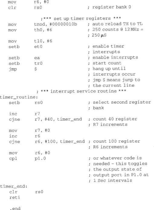
Timer/Counters
The 8051 has two 16-bit Timer/Counter registers – Timer 0 and Timer 1. When activated, these registers increment once for each event. An event can be related to the system clock (Timer) or from an external logic signal transition (Counter). If required, a Timer/Counter register can be set up to generate an interrupt when it ‘rolls over’ from all 1s to all 0s, i.e. when it reaches its full possible count of FFFFH (65535) and advances the register to 0000 on its next increment. This Timer/Counter register is called TL0 and TH0 for Timer 0 or TL1 and TH1 for Timer 1. The ‘L’ and ‘H’ refer to the low and high byte of the 16-bit register respectively.
The Timer/Counter register can be preset to any value so that any time or count limit can be set up. For example, to time or count 20 events, the register should be loaded with the number FFDCH (65616). There are several modes of operation of the Timer/Counters. The hardware inputs for the Timer/Counter channels 0 and 1 are Port pins P3.4 and P3.5 respectively.
When used as a timer, deriving its count from the system clock, it first divides that clock by 12 as in Figure 2.18.

Table 2.8
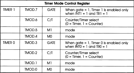
Table 2.9

The operation of Timer 0 and Timer 1 is effected by
| Timer Mode Control Register | TMOD | (address 89) |
| Timer Control Register | TCON | (address 88) |
Mode 0
This is a (virtually obsolete) mode which is included for functional compatibility with the earlier 8048 microprocessor family. In it, both Timer 0 and Timer 1 are 13-bit Counter/Timers with a divide-by-32 prescaler. The 13 bits of the Timer/Counter register are specifically:
Table 2.10

The counted input is enabled to the Timer when

If GATE = 1 then the Timer can be controlled solely by the external input INT to facilitate pulse width measurement.

Mode 1
This is the same as Mode 0, except that the Timer register is run with all 16 bits of TL0 and TH0 (or TL1 and TH1).
![]()
In this example, both channels are set up to be Timers in Mode 1. Timer 1 is to be controlled by the external pin 13, P3.3 while Timer 0 is to be controlled by the software setting of TR0. In Mode 1, both of the timers are 16 bit and so TH and TL must be loaded. Timer 1 is to be loaded with F000 and Timer 0 with D000.

The TCON timer control needs setting up, but in this example it is not proposed to use interrupts, so it becomes a simple task:
![]()
Thereafter, Timer 1 can be started with a signal on External Interrupt 1 while Timer 0 can be started with an instruction such as
![]()
For polling purposes, each byte of the Timer/Counter registers would have to be monitored. The following code locks up progress until both High and Low bytes of Timer 0 advance to zero.

The first line compares the contents of Timer register TH0 with 00 and jumps if it is not equal (to 00) to the line with the label wait1. The second line compares the contents of the Timer register TL0 with 00 and jumps if it is not equal (to 00) to the line with the label wait1. The overall effect is that the code will ‘hang up’ on these two lines until the 16-bit register TH0 and TL0 advances from its initial setting of D000 to 0000. Polling is cumbersome and wasteful of time, so all but the most trivial programs tend to use interrupts. It might be risky for the externally controlled Timer 1 to hang up in such an endless loop in case the external signal was lost or changed unexpectedly.
If the MCS51 operates from a 12 MHz clock, then timer 0 would increment every 1 ms once setb TR0 has been issued.
Mode 2
This useful mode configures the Timer register as an 8-bit Counter with automatic reload. When TL0 (or TL1) overflows, it sets the Timer Flag TF0 (TF1) and reloads TL0 (TL1) with the contents of TH0 (TH1). The reload leaves TH0 (TH1) unchanged. This mode is quite often used for baud rate generation for the serial communication port. Or, for any application which requires a regular frequency to be output. When setting up, load both TH0 and TL0 (TH1 and TL1) with the reload figure since the TL register is only reloaded when it overflows. Otherwise, the first timing run could be slightly longer if the TL register is at its reset value of 00.
Mode 3
This mode affects the two timers in different ways.
Timer 1 in Mode 3 simply stops counting. The effect is the same as setting TR1 = 0.
Timer 0 in Mode 3 splits the TL0 and TH0 registers into two independent 8-bit counter timers. TL0 is controlled in exactly the same way as in Mode 1, i.e. using control bits C/T GATE and TR0. TH0 can only act as a timer and uses the Timer 1 control functions TR1 and TF1. Timer 1 loses its ability to generate interrupts if Timer 0 is set into Mode 3. However, this mode finds a use in the circumstances when an extra Timer function is required.
Timer Example: A 50 Hz Square Wave
The following example shows how to generate a 50 Hz square wave on Port 1 bit 0. 50 Hz requires a 10 ms on and 10 ms off-cycle which can be derived from a 12 MHz clock if 10000 machine cycles are counted for each ON and each OFF period. To make a timer count up to 10000, the 16-bit register must actually be loaded with 65536 − 10000 = 55536 – which is D8F0H.


Questions
1. Two tone horn. Write a program which outputs two tones from P3.1 when the single P3.0 input goes high. The two tones should switch between 256 Hz and 440 Hz at a rate of 0.6 second intervals.
2. An alarm annunciator has 3 inputs on P1.0, P1.1 and P1.2. These are labelled and function as ALARM, ACCEPT, CLEAR. There are two outputs on P1.6 and P1.7 which provide a drive to a horn and a lamp. When the ALARM input goes high, the horn should sound a 1 kHz tone with an off–on pattern of 2 Hz. The output lamp should flash at a sound synchronized rate of 2 Hz. When ACCEPT is pressed, the alarm is cancelled and the lamp stays steady-on. When CLEAR is pressed, the system is reset with both outputs being set to ‘0’.
3. An 8051 has two inputs on P2.0 and P2.1, and uses Port 3 as an output and P2.7 as an ‘over-range’ output. The microcontroller is to time the difference between input P2.0 going high and input P2.1 going high. The basic time interval is to be LSB = 25 ms (LSB = least significant bit). The output should be displayed in binary from Port P3. If the delay exceeds the maximum counts, the over-range output should go high for 2 seconds before the system resets.
4. Write a program which outputs the frequency of a stream of pulses. Assume that the signals are input on Port P1.0. Start a timer when the input first performs a 0–1 transition, and stop the timer when the input next does a 0–1 transition. Then use the mathematical DIVIDE function to calculate the frequency of the input. For simplicity, assume that the timer never counts more than 255 between pulses (an 8 bit timer). How could this problem be extended to cope with the situation where the input stream counts up to 65535 between input pulses (a 16 bit timer?). More generally, how could the problem be extended to cope with any time interval between pulses. How could you set a ‘time-out’ to terminate the waiting after a sensible interval?
Interrupts
A CPU executes a program instruction by instruction. It will work its way through the instructions sequentially unless one of two events occurs.
1. The current instruction is an explicit command to jump a set number of instructions or to jump to a particular address.
2. An interrupt occurs. If interrupts have been enabled then that interrupt will cause the CPU to jump to a fixed location.
The 8051 has a useful vectored interrupt system that allows for 5 interrupt sources which are (in the order of priority) shown in Table 2.11.
Table 2.11
| Interrupt | Flag Name | Vector |
| External Interrupt 0 | IE0 | 0003 |
| Timer/Counter 0 | TF0 | 000B |
| External Interrupt 1 | IE1 | 0013 |
| Timer/Counter 1 | TF1 | 001B |
| Serial Port | RI + TI | 0023 |
The ‘vector’ address represents the address to which the CPU will relocate in the event of the named interrupt occurring. What will actually happen is that the Program Counter register holds the address of the next instruction to be executed. When the interrupt occurs, the Program Counter saves that next address on the memory area known as the stack and loads one of the above addresses into the Program Counter instead. If, for example, IE1 (External Interrupt 1) had been enabled and at a particular point in the program, Port 3 bit 3 (pin 13) was taken from a logic 1 to a logic 0, then an interrupt would be generated. The Program Counter would be loaded with the address 0013 and after the current instruction had finished, then the CPU would fetch its next instruction from location 0013. Each interrupt has been allocated 8 bytes, and so if the interrupt is to take more code than this, then the simplest action is to place a jmp (jump) instruction at address 0013.
The code which handles the interrupt is commonly called the interrupt service routine. The end of the interrupt service routine is terminated with the instruction reti (RETurn from Interrupt). This retrieves the return address from the stack and loads it into the Program Counter. Hence, the CPU resumes with the next instruction it was due to execute before the instruction occurred.
One last point. The vectors for the interrupt service routines are located fairly low in memory. If an interrupt doesn’t happen, then after a power-up or system reset, the CPU will quite naturally execute code from locations 0000, 0001, 0002, 0003, 0004, 0005, etc. It will quite happily work through the addresses, not knowing that the code at location 0003 contained code for External Interrupt 0. The way around this is to start the program something along the lines of

Where, for example, jmp isr_tf1 represents an instruction to jump to the piece of code labelled isr_tf1.
Here is a simple program which is designed for an 8051 operating from a 12 MHz clock and merely outputs a slow square wave from Port 1.0.

Some words must shortly be said about the nature of the 8051 stack, but first we must look at the interrupt control structure more closely. Special Function Register IP affects the priority of the interrupts. It was stated initially, that the priority of interrupts was IE0, TF0, IE1, TF1, TI + RI.
So, if all interrupts have been enabled, then if the CPU is handling <external interrupt 1> and a <timer 0> interrupt occurs, the CPU will:
However, since it has a lower priority, if a <timer 1> event occurs while the CPU is handling <external interrupt 0> then the code for isr_tf1 will just have to wait until the CPU has finished with isr_ie0. One way to alter the priority is to use the IP register. This has 5 active bits which alter the priorities according to:
| IE0 | IP.0 | External Interrupt 0 |
| TF0 | IP.1 | Timer 0 Interrupt |
| IE1 | IP.2 | External Interrupt 1 |
| TF1 | IP.3 | Timer 1 Interrupt |
| RI + TI | IP.4 | Serial Port Interrupt |
An instruction such as mov ip, #00001001B would set TF0 and RI+TI as high priority interrupts. The priority order now becomes:
Figure 2.19 shows this diagrammatically:

To enable interrupts, the Interrupt Enable (IE) register must be used.
Table 2.12


Stack
At a reset, the stack pointer is set to 07. This is an 8-bit register which is used for holding the address of a position in memory for temporary storage of data and addresses. When data is pushed onto the stack, the stack is first incremented then data is stored at that stack pointer address. A pop retrieves data from the current stack pointer address and then decrements the stack pointer. So, the first interrupt to occur would store the return address for CPU code at locations 08 and 09. Note that the default setting for the stack will cause it to overwrite the register bank 1. (Recall that Register Bank 1 sets R0–R7 as using RAM memory addresses 08–0F.) It does not overwrite the interrupt vector addresses because of the way in which the 8051 separates program code and data. Interrupt vectors would be part of the program code, whilst register banks are RAM.
The usual thing to do in any non-trivial application is to adjust the stack location, e.g.
![]()
The stack grows as necessary. Every push instruction or subroutine call or interrupt causes the next address(es) in the stack memory to be used. The limit to the size of the stack is the available data RAM.
There is an interesting modification suggested by Philips Semiconductors which allows the 8051 to seem to have 5 external interrupts. EI0 and EI1 are already known about. Two others can be created by setting Timer/Counters 0 and 1 into 8-bit Counter mode (Mode 2) with a preloaded count of FF. Thus, one more falling edge input on the Timer 0 or Timer 1 input would cause the Counter to roll over and generate an interrupt. The interrupting Counter would automatically be reloaded with FF from the TH0 or TH1 register so that the interrupt could occur again as soon as the interrupt service routing had been completed. To set up both timers for this type of operation,

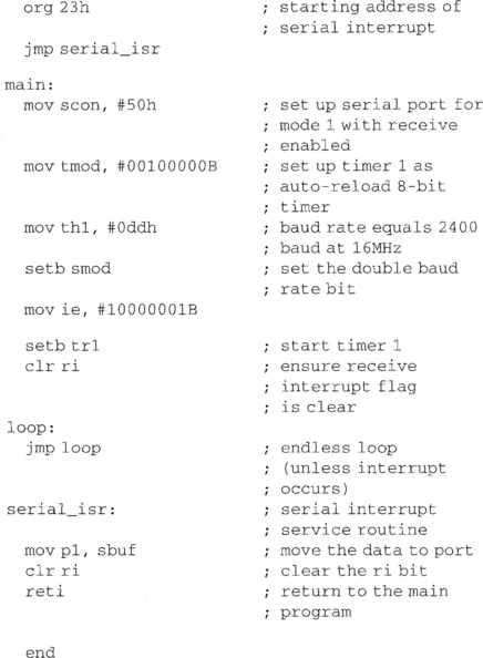
Although covered in the following section, the serial Receive Data input line can also be used to generate an interrupt in the same manner. The serial port must be set into Mode 2 (a 9-bit UART with the baud rate determined by the oscillator). The setup would be
With these parameters set up, the first 1 to 0 transition of the RxD pin would create an interrupt.
Serial Ports
The 8051 family has a full duplex serial transmission circuit. The two pins P3.0 and P3.1 have the alternate function Receive Data (RxD) and Transmit Data (TxD). Full Duplex means that it can transmit a byte of data through the TxD output at the same time as it is receiving a byte of data at the RxD input.
The most popular serial protocol is the (in)famous RS232 and this is supported by the 8051 family. P3.0 is connected to a serial to parallel converter, while P3.1 is connected to a parallel to serial converter as in Figure 2.20. The rate at which data is shifted in or out is very important in RS232 transmission. One of the Counter/Timers is usually used to set the baud rate (i.e. bits/second of transmission). For more details on the RS232 standard see Chapter 5.

Table 2.13
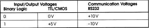
Figure 2.21 shows the MAX232 level converter connected to pins 10 (P3.0) and 11 (P3.1) to change the 8051 logic level signals into RS232-compatible voltage levels.

The serial port uses two registers and one of the timers. SCON is used for setting up and monitoring the serial port, while SBUF holds serial data. SBUF is physically two separate registers; one for holding data prior to serial transmission and one for accepting serial transmission and storing it before it is read by the CPU. Which register is accessed depends on whether the CPU performs a READ or WRITE to SBUF.
The control register SCON performs the functions listed in Table 2.14.
Table 2.14

The flexibility of RS232 is the cause of the complexity of this register. It is capable of operating in 4 modes according to the value of SM0 and SM1 Table 2.15):
Table 2.15

Mode 0: The TxD pin outputs the shift register clock (at fOSC/12) while the RxD receives and transmits the 8 bits of data. The CPU is ‘told’ to expect incoming data when RI is set to 0 and REN is set to 1.
Mode 1: Data is handled in a conventional 1 start, 8 data, 1 stop RS232 style. The 10 bits are transmitted via TxD and received via RxD.
Mode 2: This mode allows the use of parity since the 9th data bit is handled by TB8 or RB8. So in all, 11 bits are handled in the order 1 start, 8 data, RB8 (or TB8), 1 stop. It takes more effort to use since the programmer has to work out the parity of the data byte and then adjust the TB8 (or analyse the RB8) bit accordingly. This mode tends to be used for multiprocessor communication since it operates at fOSC/32 or fOSC/64 as set by the baud rate doubling bit PCON.7 (SMOD). (More of this in the following baud rate setting section.)
Mode 3: Mode 3 is the same as Mode 2 except that the baud rate is variable.
Modes 1 and 3 are used for RS232 communication: Mode 1 for 1 + 8 + 1 and Mode 3 for 1 + 8 + P + 1.
Multiprocessor Communication
Modes 2 or 3 can be programmed to act as channels for intercommunication between two or more microprocessors. This was quite an innovation when it was introduced and, while the feature still has its uses, standardization of other serial multiprocessor protocols has rendered it somewhat in a niche market. Operation is as follows:
Making bit SM2 = 1 sets up the serial port so that it will only generate an interrupt if the 9th bit received (into RB8) is a ‘1’. Hence, if an 8051 is acting as a MASTER to several SLAVES, then it may only want to address one of them. It would set TB8 to a 1 and output the address of the slave processor to which it wanted to communicate. All slaves would have an interrupt generated, and so all would be programmed to respond by looking at the received byte to see if they were being addressed. Thereafter, only the addressed slave would listen and respond to the master. All the other slaves get on with their own programs until a byte was transmitted with the 9th bit as a ‘1’.
Baud Rate Generation
RS232 conventionally uses one of a limited range of bit rates. In most cases, it is generated from the system clock and uses one of the Timers. A common method is to use Timer 1 in its Auto Reload mode. To recap, this is a mode whereby TH1 is loaded into TL1 every time TL1’s register overflows to 00. Before we detail some commonly used frequencies and their Timer load values, there is yet one more register to explain. This is PCON. PCON is the Power Control register, and the 8051 only uses 3 of its bits for internal functions and 2 bits as general-purpose flags which the programmer can utilize.
Table 2.16
| SMOD | PCON.7 | Double Baud Rate. When SMOD = 1 a double baud rate is generated if Timer 1 is used and serial mode 1, 2 or 3 is selected |
| GF1 | PCON.3 | General-purpose user flag |
| GF0 | PCON.2 | General-purpose user flag |
| PD | PCON.1 | Power Down PD = 1 activates Power Down mode until the processor is reset. The clock is stopped and minimal power is consumed. Only data held in the on-chip RAM is preserved, but all other settings are lost |
| IDL | PCON.0 | Idle. IDL = 1 disconnects the clock from the CPU but not from the Interrupt, Timer or Serial ports. All registers and settings are preserved. The processor can be woken up either by an interrupt or a full reset |
Baud Rate Generation using Timer 1
Table 2.17

The formula for calculating the TH1 value given oscillator frequency and baud rate is
TH1 = {256 – (K × Oscillator Frequency) ÷ (384 × Baud Rate)}
where K = 1 for SMOD = 0 and K = 2 for SMOD = 1.


RS422 Serial Transmission
Although the most famous, RS232 is not the only serial data standard. One of the common industrial standards which has the advantage of faster, longer haul and more reliable data transmission is the RS422. This standard uses a twisted pair differential signal to achieve 60 m at up to 10 Mbaud. None of the 8051 family have this transmission standard built in, so an example is shown in Chapter 5.
The I2C Serial Bus
Another serial standard which is available in the family is the I2C or Inter Integrated Circuit bus. This two-wire system is used for interconnecting such devices as LCD drivers, remote I/O ports, RAM, EEPROM or data converters. Many variants of the range of the 8051 family are fitted with this standard. Figure 2.22 shows a simple hardware application of the standard. Chapter 5 gives more detail of the standard and the devices which can use it.

Related to I2C is the CAN serial standard which was originally developed for the automotive industry by Bosch. The 8XCE958 and 8XC952 both have the CAN standard interface protocol as part of their I/O capability.
Bit Addressing
There is an area in the DATA RAM where each bit can be individually addressed and manipulated. Intel highlight this as the family’s ‘Boolean Processing Capability’ and many of the instructions operate on single bits. The 16 bytes from 20H to 2FH provide the 128-bit addressable locations as shown in Table 2.18.
Table 2.18

The instruction mov C, 13 loads the carry flag with the contents of bit location 13 (0CH). This corresponds to bit 5 of DATA RAM BYTE 21 otherwise known as bit 21.5 Single-bit Boolean operations would then take place with other bits with instructions such as:

Of course, these bits could be given meaningful names so that the program could start with:

In this way, binary status parameters can be stored efficiently. A common sequence might have a structure such as
A bit contrived, perhaps, but easily implemented with

Only if heat = 1, start = 1 and pump = 0 would emergency contain a 1. There are many other ways of solving this – maybe with a test such as a jc … jump if carry set etc.
Using the ADC in the 80550 Family
The 80552 family is a functional derivative of the 8051 in that it has all the same facilities and more, namely:
• 8k × 8 EPROM (83552) expandable externally to 64 kbyte
• 256 × 8 RAM expandable to 64 kbyte
• 2 standard 16-bit Timer/Counters
• 1 additional 16-bit Timer/Counter coupled to 4 capture and 3 compare registers
• 8 multiplexed analogue inputs coupled to a 10-bit ADC
• 2 8-bit Pulse Width Modulated outputs
• 5 8-bit I/O ports (plus 18-bit port shared with the analogue inputs)
Available in a 68-pin PLCC, the functional layout is shown in Figure 2.23.

The larger amount of data RAM means that the 256 locations must be split:

Obviously with more functions, the SFR gets more complex as more of its 128 bytes are needed to control and report on the status of the microcontroller.
Analogue to Digital Conversion
The analogue to digital (ADC) input circuitry consists of a 10-bit converter fed by one of 8 multiplexed inputs (from Port 5). Part of the programming process involves selection of the appropriate channel. The sucessive approximation A–D conversion process takes 50 machine cycles, which is 20 μS at a clock frequency of 12 MHz. The internal circuitry uses its own +5 V and 0 V supplies (AVDD and AVSS) which help to cut down on switching noise inherent in microprocessor circuits. The reference supplies are also brought out separately on the chip, although many designers take the simplest route of connecting ref– to the analogue 0V (which in many cases is kept as the digital 0 V) and the ref+ to either the analogue +5 supply or a separate precision reference IC.
Table 2.19


Good design principles dictate that:
• Digital and analogue grounds should be kept separate.
• The ADC reference voltage should be derived from a separate precision source.
• The analogue and digital supplies should be separately derived and controlled.
However, compromises sometimes must be reached and either through pragmatism, negligence or ignorance, you may find that because of switching noise creeping into the analogue electronics, the full 10-bit resolution is never achieved.
The result of the 10-bit conversion obviously needs two registers in which to store the result. The upper 8 bits are stored in the register ADCH and the lower 2 bits are stored in the ADC control register ADCON. Once the appropriate channel has been selected, conversion can be initiated by either a hardware signal or a software command. End of Conversion can be signalled either by an Interrupt or by polling the ADSC bit in ADCON. In more detail (Table 2.20):
Table 2.20

The most convenient way to use the converter is with interrupts. The full interrupt priority for this device is shown in Table 2.21:
Table 2.21

The vector table at the head of the code listing should be amended to include
![]()
Thereafter, setting up code such as
![]()
Conversion would be started with
![]()
When the interrupt occurs, the first task is to reset the flag:
![]()
Thereafter, the top 8 bits could be read for simplicity, or the full 10 bits could be used in whatever application is required.
If it is absolutely essential to poll the ADC rather than enable interrupts, then:
![]()
This illustrates the fact that it is impossible to perform a bit test on certain SFR registers. If the SFR register does not end in 0 or 8 then bit tests are unavailable – and ADCON is SFR register C5.
Digital to Analogue Conversion (the PWM output)
A pulse width modulated (PWM) output is available from many microprocessors: both the 805l and PIC families have members which give this useful output. Once buffered by an external amplifier, a PWM output can be used as a form of digital to analogue converter (DAC). This is often used to drive external devices such as motors. Figure 2.24 shows the effect of varying the pulse width and the way in which the average voltage applied to the external device increases as the mark:space ratio increases.
The ‘552 has two PWM output channels which generate pulses of programmable length and frequency. These are called PWM0 and PWM1. An 8-bit counter counts through the sequence 0–254 and the counter is continually compared with the contents of PWM0 and PWM1. Pulse Width Channel 0 is HIGH while the 8-bit counter is smaller than the PWM0 register. Pulse Width Channel 1 is HIGH while the 8-bit counter is smaller than the PWM1 register.
This means that if the PWM0 register is loaded with (say) 63 then the Channel 0 output will be HIGH while the Counter is lower than, or equal to, this value and LOW while the Counter is higher than this value. The averaged channel output is thus proportional to the contents of the corresponding PWM register. There is also a register PWMP which is a prescalar to set the repetition frequency of the output. The repetition frequency is given by:
fPWM= fOSC/(2 × (1 + PWMP) × 255)
By loading PWMP with different values, a repetition frequency range of 92 Hz to 23.5 kHz can be obtained with a 12 MHz clock. By loading the PWM registers with either 00 or FF, the PWM output channels will output a constant HIGH or LOW level respectively. There are no other controls for the PWM outputs and the output pins themselves are not used for any other purpose. Software operation is simple.
![]()
Alternatively, a ramp could be generated using code which incremented or decremented the PWM0 or PWM1 registers. Care would need to be taken that the register was not incremented at a rate faster than the pulse repetition frequency, so it is frequently implemented in a timer interrupt routine. A simple command such as inc PWM0 would have the desired effect.
The 80552 Watchdog Timer
The Watchdog Timer is enabled by connecting the /EW input pin (pin 6) to 0 V. It cannot be disabled by software. Timer T3 is used to implement the Watchdog Timer. It is an 8-bit timer (direct address FFH) which, if allowed to overflow, will RESET the ‘552. The timer is incremented every 12 × 2048 × 1/fOSC seconds, ≈ 2 ms with a 12 MHz clock.
The 8-bit timer T3 can be preloaded with numbers to give a watchdog interval of between 2 ms and 524 ms from a 12 MHz clock.
Bit 4 in the PCON control register is used to restart the Watchdog with the new value loaded into the T3 register. Hence the code
![]()
will set the maximum timeout from the Watchdog. This code needs to be repeated at intervals of not more than the 524 ms needed for a 12 MHz clock. In practice, the two lines of code would be embedded into a subroutine such as
![]()
This would be tucked away with the subroutines in their usual position at the end of the program and could be called with an instruction such as
![]()
If a shorter watchdog period is required, then (for example) mov T3, #206 would be incremented 50 times before overflow and hence would give a WDT period of 100 ms from a 12 MHz clock.
Parallel Expansion
A common I/O device used in the Intel families is the 8255 Programmable Peripheral Interface (PPI). This 40-pin IC has three 8-bit programmable I/O ports. The control can be seen to be fairly straightforward, as it requires:
• 2 address lines (to discriminate between the various output ports)
Figure 2.25 shows how the MCS51 family could be interfaced. Note that it is treated as external DATA RAM in that information is both written to it and read from it. The decoder could be combinational logic or a PLD set up to select the 8255 whenever the correct address was output at the same time as a /RD (read) or /WR (write) signal.

This implies that it occupies a portion of DATA RAM – and the programmer must not forget which address it uses and inadvertently try to read/store data at that location.
An 8255 PPI requires 4 × 8-bit addresses:
This is why there are 2 address lines required. To decode for addresses see Table 2.22.
Table 2.22
| Port A | E0 | 11100000 |
| Port B | E1 | 11100001 |
| Port C | E2 | 11100010 |
| Port D | E3 | 11100011 |
Then a logic circuit similar to Figure 2.26 would need to be used.

The 8051 is unusual in having quasi-bidirectional ports, and as such they do not require to be given data direction information prior to their use. Like many other interface ICs (and microcontrollers count as that) the 8255 needs to be told which ports are to act as inputs and which as outputs. This information needs to be sent to the Control Port prior to any ports being used. Another old-style feature of the 8255 is that it is not bit programmable. This means that Port A must be wholly programmed as an output or an input port. The same applies for Port B. However, Port C can be nibble programmed, i.e. the upper nibble can be an output while the lower nibble can be an input.
The 8255 control byte should be
![]()
Sending the binary word 10001010 to the control port would result in
| Port A | Output |
| Port B | Input |
| Port C upper | Input |
| Port C lower | Output |
The mode bits set the different handshake requirements but for straightforward uncontrolled nibble/byte transfer, Table 2.23 would suffice:
Table 2.23

To output binary data 01010101 on Port A as previously programmed, use the sequence:
![]()