
Appendices
A MCS51 Instruction Set
| Rn | Register R7–R0 of currently selected register bank |
| direct | 8-bit internal data location’s address |
| @Ri | Internal RAM location 0–255 addressed indirectly through R7–0 |
| #data | 8-bit constant included in instruction |
| #data16 | 16-bit constant included in instruction |
| addr16 | 16-bit destination address (used in LCALL & LJMP) |
| addr11 | 11-bit destination address (used in ACALL & AJMP) |
| rel | Signed (2’s complement) 8-bit offset byte (SJMP) |
| bit | Direct addressed bit in internal data RAM or Special Function Register |
Arithmetic Operations
| ADD | A,Rn | Add register n to A |
| ADD | A,direct | Add direct byte to A |
| ADD | A,@Ri | Add indirect RAM to A |
| ADD | A,#data | Add immediate data to A |
| ADDC | A,Rn | Add with carry Register n to A |
| ADDC | A,direct | Add with carry direct byte to A |
| ADDC | A,@Ri | Add with carry indirect RAM to A |
| ADDC | A,#data | Add with carry immediate data to A |
| SUBB | A,Rn | Subtract with borrow Register n from A |
| SUBB | A,direct | Subtract with borrow direct byte from A |
| SUBB | A,@Ri | Subtract with borrow indirect RAM from A |
| SUBB | A,#data | Sub. with borrow immediate data from A |
| INC | A | Increment Accumulator |
| INC | Rn | Increment Register n |
| INC | direct | Increment direct byte |
| INC | @Ri | Increment indirect RAM |
| DEC | A | Decrement Accumulator |
| DEC | Rn | Decrement Register n |
| DEC | direct | Decrement direct byte |
| DEC | @Ri | Decrement indirect RAM |
| INC | DPTR | Increment Data Pointer |
| MUL | AB | Multiply A & B |
| DIV | AB | Divide A by B |
| DA | A | Decimal Adjust Accumulator |
Logical Operations
| ANL | A.Rn | AND Register n to A |
| ANL | A,direct | AND direct byte to A |
| ANL | A,@Ri | AND indirect RAM to A |
| ANL | A,#data | AND immediate data to A |
| ANL | direct,A | AND A to direct byte |
| ANL | direct,#data | AND immediate data to direct byte |
| ORL | A.Rn | OR Register n to A |
| ORL | A,direct | OR direct byte to A |
| ORL | A,@Ri | OR indirect RAM to A |
| ORL | A,#data | OR immediate data to A |
| ORL | direct,A | OR A to direct byte |
| ORL | direct,#data | OR immediate data to direct byte |
| XRL | A.Rn | Ex-OR Register n to A |
| XRL | A,direct | Ex-OR direct byte to A |
| XRL | A,@Ri | Ex-OR indirect RAM to A |
| XRL | A,#data | Ex-OR immediate data to A |
| XRL | direct,A | Ex-OR A to direct byte |
| XRL | direct,#data | Ex-OR imm. data to direct byte |
| CLR | A | Clear A |
| CPL | A | Complement A |
| RL | A | Rotate A Left |
| RLC | A | Rotate A Left through Carry |
| RR | A | Rotate A Right |
| RLC | A | Rotate A Right through Carry |
| SWAP | A | Swap nibbles within A |
Data Transfer
| MOV | A,Rn | Move Register n to A |
| MOV | A,direct | Move direct byte to A |
| MOV | A,@Ri | Move indirect RAM to A |
| MOV | A,#data | Move immediate data to A |
| MOV | Rn,A | Move A to Register n |
| MOV | Rn,direct | Move direct byte to Register n |
| MOV | Rn,#data | Move immediate data to Register n |
| MOV | direct,A | Move A to direct byte |
| MOV | direct,Rn | Move Register n to direct byte |
| MOV | direct,direct | Move direct byte to direct byte |
| MOV | direct,@Ri | Move indirect RAM to direct byte |
| MOV | direct,#data | Move immediate data to direct byte |
| MOV | @Ri,A | Move A to indirect RAM |
| MOV | @Ri,direct | Move direct byte to indirect RAM |
| MOV | @Ri,#data | Move immediate data to indirect RAM |
| MOV | DPTR,#data16 | Load data ptr with a 16-bit const |
| MOVC | A,@A+DPTR | Move code byte rel. to DPTR to A |
| MOVC | A,@A+PC | Move code byte relative to PC to A |
| MOVX | A,@Ri | Move external RAM (8-bit) to A |
| MOVX | A,@DPTR | Move external RAM (16-bit) to A |
| MOVX | @Ri,A | Move A to external RAM (8-bit) |
| MOVX | @DPTR,A | Move A to external RAM (16-bit) |
| PUSH | direct | Push direct byte onto the stack |
| POP | direct | Pop direct byte from stack |
| XCH | A,Rn | Exchange register n with A |
| XCH | A,direct | Exchange direct byte with A |
| XCH | A,@Ri | Exchange indirect RAM with A |
| XCHD | A,@Ri | Exch. low-order digit ind. RAM with A |
Boolean Variable Manipulation
| CLR | C | Clear carry |
| CLR | bit | Clear direct bit |
| SETB | C | Set carry |
| SETB | bit | Set direct bit |
| CPL | C | Complement carry |
| CPL | bit | Complement direct bit |
| ANL | C,bit | AND direct bit to carry |
| ANL | C,/bit | AND complement of direct bit |
| ORL | C,bit | OR direct bit to carry |
| ORL | C,/bit | OR complement of direct bit |
| MOV | C,bit | Move direct bit to carry |
| MOV | bit,C | Move carry to direct bit |
| JC | rel | Jump if carry set |
| JNC | rel | Jump if carry not set |
| JB | bit,rel | Jump if direct bit set |
| JNB | bit,rel | Jump if direct bit not set |
| JBC | bit,rel | Jump if direct bit is set and clear bit |
Program Branching
| ACALL | addr11 | Absolute subroutine call |
| LCALL | addr16 | Long subroutine call |
| RET | Return from subroutine | |
| RETI | Return from interrupt | |
| AJMP | addr11 | Absolute jump |
| LJMP | addr16 | Long jump |
| SJMP | rel | Short jump (relative addr) |
| JMP | @A+DPTR | Jump indirect relative to the DPTR |
| JZ | rel | Jump if A is zero |
| JNZ | rel | Jump if A is not zero |
| CJNE | A,direct,rel | Comp dir byte to A and jump if not eq. |
| CJNE | A,#data,rel | Comp imm to A and Jump if not eq. |
| CJNE | Rn,#data,rel | Comp imm to reg n and jump if not eq. |
| CJNE | @Ri,#data,rel | Comp imm to ind and jump if not eq. |
| DJNZ | Rn,rel | Dec register n and jump if not zero |
| DJNZ | direct,rel | Dec direct byte and jump if not zero |
| NOP | No operation |
The Special Function Register
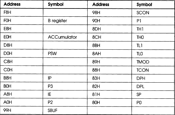
B register: This is mostly used in multiply and divide operations. If not required for these functions, the memory space is available.
PSW (Program Status Word): CY AC F0 RS1 RS0 0V – P
Table A.2
| CY | PSW.7 | Carry Flag: set/cleared by hardware or software during certain arithmetic and logical instructions |
| AC | PSW.6 | Auxiliary Carry Flag: set/cleared by hardware during addition or subtraction instructions to indicate carry or borrow out of bit 3 |
| F0 | PSW.5 | Flag0: set/cleared/tested by software as a user-defined status flag |
| RS1 | PSW.4 | Register bank select control bits |
| RS0 | PSW.3 | |
| 0V | PSW.2 | Overflow flag: set/cleared by hardware during arithmetic instructions to indicate overflow conditions |
| – | PSW.1 | (reserved) |
| P | PSW.0 | Parity Flag: set/cleared by hardware each instruction cycle to indicate an odd/even number of ‘one’ bits in the accumulator |
IP (Interrupt Priority): These set the priority of the 5 interrupt sources. There are two priority levels: low and high. A 0 in the bit position is a low priority, while a 1 sets a high priority. Within each priority level, the order of evaluation of simultaneous interrupts is
| IE0 | IP.0 | External interrupt 0 |
| TF0 | IP.1 | Timer 0 interrupt |
| IE1 | IP.2 | External interrupt 1 |
| TF1 | IP.3 | Timer 1 interrupt |
| RI + TI | IP.4 | Serial port interrupt |
P3 (Port 3): A general-purpose Input/Output port. It has the following alternate functions shown in Table A.3.
Table A.3
| RD | P3.7 | Read data control output. Active low pulse generated by hardware when external data memory is read |
| WR | P3.6 | Write data control output. Active low pulse generated by hardware when external data memory is writtten |
| T1 | P3.5 | Timer/Counter 1 external input or test pin |
| T0 | P3.4 | Timer/Counter 0 external input or test pin |
| INT1 | P3.3 | Interrupt 1 input pin. Low-level or falling edge trigger |
| INT0 | P3.2 | Interrupt 0 input pin. Low-level or falling edge trigger |
| TXD | P3.1 | Transmit Data pin for serial port in UART mode. Clock output in shift register mode |
| RXD | P3.0 | Receive Data pin for serial port in UART mode. Data I/O pin in shift register mode |
IE Interrupt Enable register
Table A.4
| EA | IE.7 | Enable All control bit: cleared by software to disable all interrupts, independent of the state of IE.4–IE.0 |
| – | IE.6 | |
| – | IE.5 | |
| ES | IE.4 | Enable serial port control bit: set/cleared by software to enable/disable interrupts from TI or RI flags |
| ET1 | IE.3 | Enable Timer 1 control bit: set/cleared by software to enable/disable interrupts from Timer/Counter 1 |
| EX1 | IE.2 | Enable External interrupt 1 control bit: set/cleared by software to enable/disable interrups from INT1 |
| ET0 | IE.1 | Enable Timer 0 control bit: set/cleared by software to enable/disable interrupts from Timer/Counter 0 |
| EX0 | IE.0 | Enable External interrupt 0 control bit: set/cleared by software to enable/disable interrupts from INT0 |
P2 Port 2: SCON Serial Port Control/Status Register.
Table A.5
| SM0 | SCON. 7 | Serial port mode control bit 0; set/cleared by software |
| SM1 | SCON.6 | Serial port mode control bit 1: set/cleared by software |
| SM2 | SCON.5 | Serial port mode control bit 2: set by software to disable reception of frames for which bit 8 is zero |
| REN | SCON.4 | Receiver Enable control bit: set/cleared by software to enable/disable serial data reception |
| TB8 | SCON.3 | Transmit bit 8: set/cleared by hardware to determine state of ninth data bit transmitted in 9-bit UART mode |
| RB8 | SCON.2 | Receive bit 6: set/cleared by hardware to indicate state of ninth data bit received |
| TI | SCON.1 | Transmit Interrupt flag: set by hardware when byte transmitted. Cleared by software after servicing |
| RI | SCON.0 | Receive interrupt flag: set by hardware when byte received. Cleared by software after servicing |
| SM0 | SM1 |
| 0 | 0 Shift register I/O expansion |
| 0 | 1 8-bit UART variable data rate |
| 1 | 0 9-bit UART fixed data rate |
| 1 | 1 9-bit UART variable data rate |
P1 (State of Port 1): TCON Timer/Counter Control/Status Register
Table A.6
| TF1 | TCON.7 | Timer 1 overflow flag: set by hardware on Timer/Counter overflow. Cleared when interrupt processed |
| TR1 | TCON.6 | Timer 1 run control bit: set/cleared by software to turn Timer/Counter on/off |
| TF0 | TCON.5 | Timer 0 overflow flag: set by hardware on Timer/Counter overflow. Cleared when interrupt processed |
| TR0 | TCON.4 | Timer 0 run control bit: set/cleared by software to turn Timer/Counter on/off |
| IE1 | TCON.3 | Interrupt 1 edge flag: set by hardware when external interrupt edge detected. Cleared when interrupt processed |
| IT1 | TCON.2 | Interrupt 1 type control bit: set/cleared by software to specify falling edge/low level triggered external interrupts |
| IE0 | TCON.1 | Interrupt 0 edge flag: set by hardware when external interrupt edge detected. Cleared when interrupt processed |
| IT0 | TCON.0 | Interrupt 0 type control bit: set/cleared by software to specify falling edge/low level triggered external interrupts |
SP (Stack Pointer): At a reset, the stack pointer is set to 07. When data is pushed onto the stack, the stack is first incremented, then data is stored at that stack pointer address. A pop retrieves data from the current SP address and then decrements the stack pointer. Note that the default setting for the SP will cause it to overwrite the Register bank 1.
B Number Systems
Computers deal in binary quantities, i.e. a ‘low’ voltage (0 V–0.8 V) is a logic ‘zero’ while a ‘high’ voltage (3.4 V–5.0 V) is a logic ‘one’. Humans work in a decimal system, and as such you probably learned your maths as Hundreds, Tens and Units (HTU). Mathematically, we could express this as 102, 101, 100, so a sum would be:

Note that adding 6 tens to 8 tens generates a ‘carry’, i.e. it overflows the capability of the tens column.
The same happens in the binary scale. We do not have Hundreds, Tens and Units, but we do have powers of 2:
![]()
A decimal system has 10 symbols (0123456789) while the binary system has 2 (01).
Conversion: Binary → Decimal
A binary number can simply be converted to decimal by noting the position and value of the 1s:

Conversion: Decimal → Binary
A common way of converting decimal numbers to binary is to use the ‘repeated division by 2 method’. For example, to convert 20710 into binary:

The initial number is repeatedly divided by 2 until either a ‘1’ or a ‘0’ is left. At each stage, the remainder is written down, i.e. 207 divided by 2 is 103 r 1 etc. The answer is then read from bottom to top, i.e. 20710 = 110011112.
Hexadecimal Notation
Computers work in binary quantities, and also handle words of various sizes. These could be 4, 8, 16, 32 or even 64 bits wide. In this book, we are concerned mostly with 8-bit processors. 8 bits are known as a byte, while 4 bits are known as a nibble. 4 bits contain 16 possible binary numbers, so it has become convenient to use a numbering system called hexadecimal. In this system there are 16 single symbols: 0 1 2 3 4 5 6 7 8 9 A B C D E F. Our ‘HTU’ sum has now become
![]()
Conversion: Decimal → Hexadecimal
Given a number such as 237, it will be found that 237 divided by 16 is 14 r 13. 14 has a hexadecimal value of E. 13 has a hexadecimal value of D. So, 23710 = ED16.
Conversion: Hexadecimal → Decimal
Conversion of a number such as 7A requires the use of both number systems, i.e. A has a decimal value of 10, 7 in the 161 column has a decimal value of 7 × 16 = 112. 7A16 = 11210 + 1010 = 12210.
Of course, the simple way to convert is to use the convert facility available on most calculators. But there is no reason for not knowing the mechanism behind the conversion principle.
This section is concerned with the manipulation of 8-bit binary and hexadecimal numbers. It deals with the various ways in which numbers can be combined.
Logic
There are four main logical fuctions: AND, OR, NOT, EXCLUSIVE OR. They are defined as follows:


The following examples show the effects of two 8-bit numbers being combined.


Applications of Logic Functions
Masking: It is sometimes necessary to SET (to 1) or RESET (to 0) a single bit of an 8-bit byte. This is done by a process called masking. For example, if it is necessary to set bit 3 of a byte, then that byte should be ORed with:
00001000 (note that bit 0 is the Least Significant Bit (LSB))
This is known as the mask byte. When any two numbers are ORed together, a 1 in any position causes a 1 in the output. This mask byte would cause bit 3 to be set to 1, i.e. if the byte was

If a bit needs to be RESET, the AND function is used. ANDing a number with 11110111 would cause bit 3 to be RESET and all others to be left unchanged. This is because 0 ANDed with 1 = 0, 1 ANDed with 1 = 1, while 0 ANDed with 0 = 0 and 1 ANDed with 0 = 0.
For example, to reset bit 7 – AND with 01111111.

If the supplied byte was 11000110 then the result would be 01000110, i.e. unchanged apart from bit 7.
Occasionally, it is necessary to change the state of one or more bits. The simplest way to do this is with the EXCLUSIVE-OR function.
The mask on the lower half of the sum modifies the original byte as shown. When the mask bit is ‘0’ the source bit is unchanged, and when the mask bit is ‘1’, the source bit is complemented.

Arithmetic
You have probably grasped the practicalities of decimal addition quite well by now. Adding 27 to 31 is easy, but given 89 added to 47, then you have to start using the concepts of ‘carries’. The same occurs in binary:
![]()
(In decimal 1 + 1 = 2, which is binary 10.)
If a carry is involved, then 1 + 1 + 1 = 1 carry 1 (in decimal, 1 + 1 + 1 = 3 which is binary 11).
Subtraction
Subtraction involves the concept and possibility of negative numbers. An integer byte as used so far does not deal in negative numbers, so the theory must be altered. The number system is altered so that the Most Significant Bit (MSB) – which is bit 7 in a byte – is used to indicate the sign of the number. 10000000 is the smallest number which is −128, while 01111111 is the largest number which is +127.
The process of converting a positive to a negative number is called ‘taking its 2’s complement’. The process of handling numbers which indicate positive and negative numbers is called ‘2’s complement arithmetic’.
| For example, form the 2’s complement of → | 01101001 | 105 |
| 1’s complement = | 10010110 | |
| add 1 = | 00000001 | |
| result | 10010111 | (−)23 |
The ‘–23’ refers to the fact that the negative version of ‘105’ is 23 up from the maximum negative number of −128. (Work it out and see!)
To subtract 105 from 123, the procedure is to convert 105 into its negative equivalent and then add the two numbers.
| 105 in binary | 01101001 | |
| 2’s complement | 10010111 | |
| 123 in binary | 01111011 | |
| addition | 00010010 | = 18 |
Binary Coded Decimal
Binary Coded Decimal (or BCD) is another binary encoding scheme which encodes each decimal digit into a 4-bit binary code. It is a somewhat inefficient method since only 10 of the possible 16 codes are used. However, it finds a very important use where numeric displays are involved. For example, calculators, tills etc. An 8-bit byte would be encoded as:
![]()
Gray Code
This is commonly used for mechanical shaft-angle encoders, among other things. It has the property that only one bit changes in going from one state to the next. This prevents errors, since with conventional binary, there is no way of guaranteeing that all bits will change simultaneously at the boundary between two encoded values. For example, in going from 7 (0111) to 8 (1000), as a mechanical shaft rotates, it could be possible to generate 15 (1111) for a very short period of time.
Gray code avoids this. A 4-bit Gray code would be:

American Standard Code for Information Interchange (ASCII)
Whenever characters, numbers and other codes need to be send from one device to another, it is frequently encoded into ASCII. Originally, this was a 7-bit code, but now has been extended into an 8-bit code to cover a greater variety of symbols. Most of the codes are directly for symbols, but the first 32 are used as control characters. They control things like serial transmission of data, or printers, or file exchange (see page 189).
Table B.1

