Chapter 4
Add a LoRa Radio to a Raspberry Pi Zero
A recent phenomenon in the Internet of Things area is the proliferation of new, long-reaching radio modules, in particular LoRa radios that can transmit data more than 10km in the open ISM radio bands (434 and 912MHz in the United States, 868MHz elsewhere). Also, the $10 Raspberry Pi Zero is a great option when you need to embed more computing power than a microcontroller in a project. In this chapter we will use surface-mount parts to design an EAGLE library for a LoRa radio module, and then connect it to a Raspberry Pi Zero (see Table 4-1).
Table 4-1: LoRa for Pi bill of materials
| Part | Source | Price ($) |
| (1) RFM95 LoRa radio module | Digi-Key 1597-1488-ND | 7 |
| (1) 10k SMT 1206 resistor | Digi-Key 311-10.0KFRCT-ND | .01 |
| (1) 10uF SMT 1206 capacitor | Digi-Key 587-1352-1-ND | .10 |
| (1) .1uF SMT 1206 capacitor | Digi-Key 399-5615-1-ND | .05 |
| (1) SMA antenna edge connector | Digi-Key CON-SMA-EDGE-S-ND | 1.77 |
| (1) 2×20 female header | 4UCON | .35 |
The finished product is shown in Figure 4-1.

Figure 4-1: The finished board, with custom artwork on the silkscreen layer and the top solder mask layer, as described in this chapter
Designing an EAGLE Library
An EAGLE library is a collection of devices, so it may be more accurate to say that we’re designing an EAGLE device in this chapter—a device that will reside in its own library. In EAGLE, a device has three components:
- Symbol: This is the representation of the device that appears in the schematic view. It describes the interfaces and signals of the part, and it provides pins to hook it up to other parts.
- Package: This how the part appears in the board design tool, and it corresponds to the physical form factor of the part. The package provides holes or pads for connecting the part by traces to other parts. A device can come in several different packages.
- 3D package: EAGLE version 8 is much more integrated with Autodesk’s Fusion 360; each library package part can have a 3D model attached to it. The 3D model can be created in Fusion 360 or in EAGLE’s built-in tool, or it can be imported from 3D tools like SketchUp.
Start EAGLE on your computer. Select File → New → Library to open a dialog box showing the various components of the library part. We’ll start with the symbol. The Add symbol will bring up a layout tool with a similar but slightly different toolbox than the Schematic Editor.
When creating a device, you’ll need to have access to the datasheet for the part in question, and you’ll have to do a little hunting to find the information necessary to interpret the part as a device. At a minimum, you’ll be looking for a table showing the pin numbering and functions, and a mechanical drawing showing the size of the part and pads. You may also find suggested application notes that will provide minimal hookup circuits and recommendations for filters and such.
For example, the HopeRF LoRa RFM95 module we will be using has a 121-page datasheet that can be downloaded from Digi-Key or the manufacturer (it’s also in the GitHub repo): www.hoperf.com/upload/rf/RFM95_96_97_98W.pdf.
Figure 4-2 shows the module and the pin assignments, which appear on page 10 of the datasheet and are described in more detail on page 11.

Figure 4-2: The pin descriptions from the module’s datasheet. Note that pin numbering is counterclockwise from the upper-left pin 1.
Creating the Symbol
With this diagram in hand, we can start laying out the schematic symbol for the part. Start with the Pin tool. Pins are connection points for signals; they have one side with a “hot spot” for making connections that should be facing outward from the part.
You have a lot of leeway in how you lay out your symbol; it doesn’t have to correspond to the physical layout and, in fact, usually shouldn’t.
Note that pins have default names numbered by the order they were placed. Use the Name tool to change these names to the physical pin that the signal corresponds to. Doing so will help later when connecting the symbol to the package, and the names will also appear on the schematic next to the pin to indicate the mapping (see Figure 4-3).
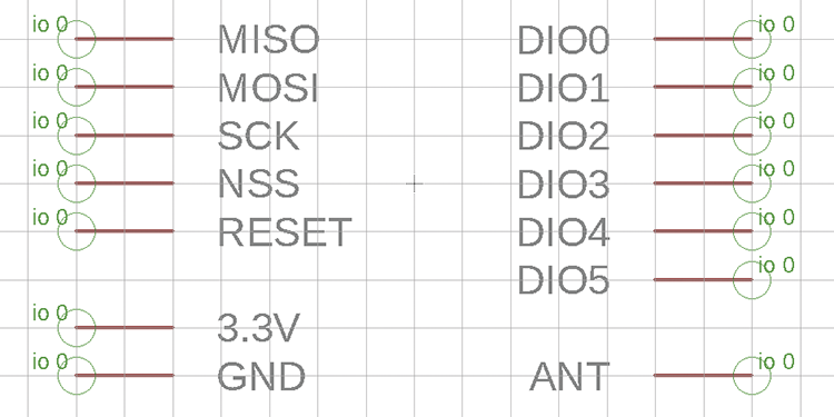
Figure 4-3: Adding pins. Group pins functionally in the schematic symbol. In this case, all the module’s IO pins are together on the right, the SPI communication interface is on the left, and power and the antenna are at the bottom.
Use the Line tool to draw a box around the pin labels. Add a label with the Text tool.
Each of the pins can be given additional attributes that help EAGLE apply the design rules when checking your circuit for correctness (see Figure 4-4). For example, each of the pins in the symbol can have their directionality marked as inputs, outputs (or both), or power pins. Use the Info tool to change the direction attribute of the 3.3V and GND pins to PWR. This enables additional design checks; you could also change the direction of the other pins to match the table on page 11 of the datasheet.

Figure 4-4: When you set the direction parameter, you indicate that the power pins are in a special class. This allows EAGLE to make additional checks with the design rules.
Save the library; by default it will be saved in the lbr directory of your EAGLE installation. EAGLE libraries are XML files with an eagle.dtd doctype and an .lbr extension. EAGLE also periodically autosaves your work in a file in the same directory with a .l#1, .l#2, etc. extension.
Creating the Package
Now let’s move on to the package, which is what will appear in the board view. Some parts can have the same symbol but come in various standard packages; you may see package names like SOT23, DIP, DPACK, and QFN. The RFM module is in its own custom package footprint, so call it something like RFM95_MODULE in the Library Manager.
For the package, we need to find the mechanical drawing of the part in the datasheet. Usually it is toward the end of the document; for the RFM95 module, refer to the package drawing on page 120 of the datasheet (see Figure 4-5).

Figure 4-5: Mechanical drawings for parts can range from the verbose to the cryptic. This datasheet sketch is somewhere in between, with a couple of ambiguous dimensions, like the pad size on the module and tolerances for variations in parts.
Some notes on interpreting mechanical drawings:
- They are almost always in millimeters (mm) unless otherwise specified. Sometimes Imperial dimensions aren’t labeled as such but appear in parentheses.
- Sometimes there is a suggested land pattern, and sometimes you need to calculate some dimensions.
- In some cases, there may be additional application notes for ground planes for heat dissipation.
- When in doubt, get out some calipers and measure the actual part.
- After you draw a land pattern, print it out to scale and place the actual part on the paper as a sanity check.
The RFM95 module is 16mm square, and there are eight pads per side. By measuring the pads on the actual module, you’ll find they are just about 1.5mm wide and a little more than 1.5mm long. The datasheet says the pitch of the pads is 2mm on center, which leaves .5mm between each pad. We will make pads that the module can sit on, with a little bit of pad sticking out the side so the module can be soldered by hand if needed. The pads will be 1.5mm×3mm so that they can be easily centered on the module outline.
Start by setting the grid to something that matches the pad pitch. In this case we can set a 1mm grid. Use the default pad size to lay out 16 pads, as in Figure 4-6.
A few notes on pad placement:
- Numbering starts with 1 in the upper left, then incrementing counterclockwise.
- Use the Pad tool and set the dimension to the default (we’ll change the pad size in a minute).
- Start at coordinate (–8, 15), and then place the pads 2mm apart on the y-axis. Note that you should start at 15 because the center of the pad is 1mm from the edge, as shown in the datasheet.
- As you place the pads, move counterclockwise.
When you’re done, pin 1 should be in the upper left, pin 9 in the lower right, and pin 16 in the upper right. We’ll use these pin numbers later to hook up to the symbol, so they have to be correct. Confirm with the Info tool if you need to.

Figure 4-6: Placing the default-sized pads
Now we’ll resize the pads using the Change Object Properties tool. Go to the SMD submenu (for surface-mount pads) and select the ellipsis (…), which allows you to type in a user-defined option. In the dialog box that appears, type 3 x 1.25 (that’s width × height using the units set by the grid). After you click OK, you won’t get much feedback that the tool is active, but move your crosshair over the origin of each of the pads (note, as mentioned in Chapter 2, that the TOrigins layer must be active) and click on a pad to change its dimensions. It should look like Figure 4-7. Note that the pad names will be easier to read when the pads are larger; double-check them now.

Figure 4-7: Resizing the pads with the Change Object Properties tool
Pads will have default names like P$1; you can rename them to match the mapping of the schematic pins to the pads on the board layout.
Change the layer to tPlace and draw in the outline of the module; this layer shows the dimensions of components for placement. Add a dot on pin 1 and some descriptive text for landmarks on the board (like the antenna). Confirm that the bounding box is 16mm×16mm as specified in the datasheet.
Connecting the Symbol and Package in a Device
Next we will create a device definition, which makes connections between the symbols and packages of the library. In the Library Manager, select Add Device and name it something like RFM95_RADIO_MODULE. You’ll see the device connection panel, as shown in Figure 4-8.

Figure 4-8: The device connection panel
First, add the RFM95 symbol to the left pane using the Add Symbol tool. Add the RFM95_MODULE to the right pane by selecting New → Add Local Package. Then connect all of the signal pins of the symbol to the pads of the package by clicking the Connect button. When everything is connected, the dialog box should look like Figure 4-9.
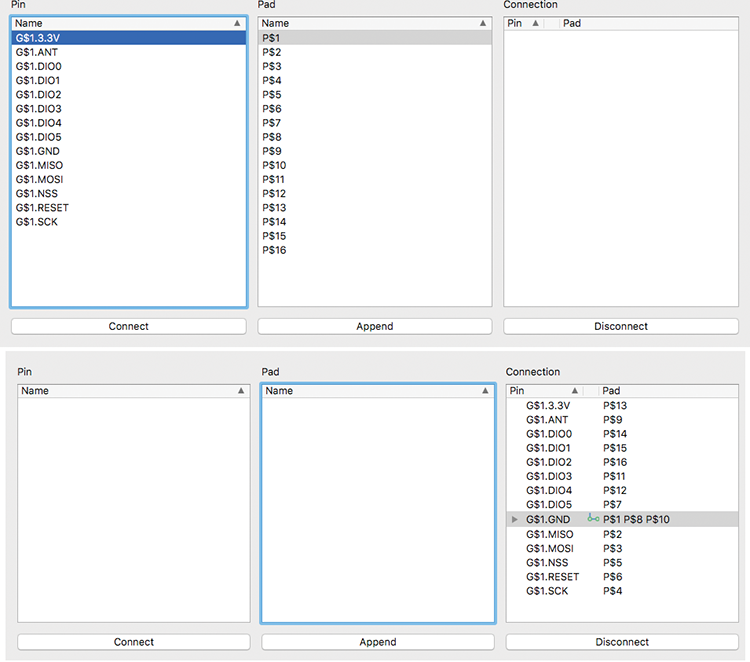
Figure 4-9: Connecting pins to signals. Use the Append option to connect the multiple grounds (pins 1, 8, and 10) together.
Using the New Device in a PCB Design
Now you’re ready to use the library. Restart EAGLE to load the library automatically or load the library by choosing Library → Open Library Manager → Use. We’ll also be using the Raspberry Pi Zero library included in the GitHub repository, so load that as well if you haven’t already.
To create the schematic, you’ll follow the process of placing symbols described in Chapter 3. Start with the RFM95 module. The Pi will communicate with the radio module using the SPI serial communications pins. This is a three-wire communications protocol (with a fourth chip select line).
Connect signals to
- MOSI: Master Out/Slave In
- MISO: Master In/Slave Out
- SCK: Data clock
- NSS: Chip select. This requires a 10k pull-up resistor so it won’t be in a floating state.
The datasheet recommends a .1μF filter capacitor close to the power pin on the RFM module, so add that. These will all be surface-mount parts in the large, easy-to-hand-solder 1206 format (0603 would be more common in production to save space). Add a 10μF capacitor between power and ground as well to act as a charge store for when the radio transmits. The radio part of the schematic should look like Figure 4-10.
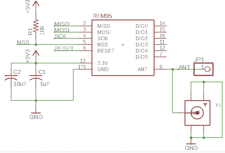
Figure 4-10: Using the RFM95 radio module in a schematic. Connecting the signals (top), then adding a pull-up resistor, a couple of capacitors to power, and a coax antenna connector.
Next, add the Raspberry Pi part from the library. You’ll notice that the schematic labels all the pins on the 40-pin Raspberry Pi header. Find the SPI pins on the Pi (19, 21, and 23) and connect them by drawing a signal and labeling it the same as on the radio module. Connect the NSS select line to pin 31 (GPIO6) and the radio reset to 33 (GPIO13). These will match the radio control code that can be used later. Next, hook up power and ground and you’re finished with the schematic (see Figure 4-11).
Switch to the board view and move the parts onto the work area. The Pi library device has an outline on the dimension layer, so you can delete the default dimension lines and EAGLE will figure out the board shape based on the library part. Place the parts something like in Figure 4-12.
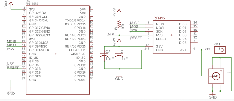
Figure 4-11: The finished Raspberry Pi Zero and radio module schematic

Figure 4-12: Placing the parts on the board
Route the top signals as in Figure 4-13. We’re going to add a ground plane, so don’t worry too much if your ground signals are all messy; they’ll all be combined into a single plane later.
Next, route the bottom signals (Figure 4-14). In this case, only +3V and GND will be on the bottom.
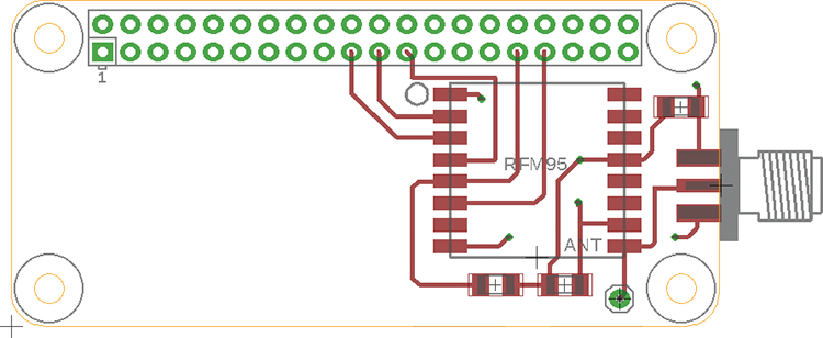
Figure 4-13: Routing the top signals
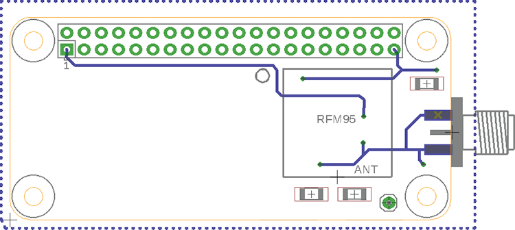
Figure 4-14: Routing the bottom signals
Adding a Ground Plane
EAGLE allows you to draw polygons into layers and give them signal names. Using the Ratsnest tool, the named polygon areas will all be unioned together into a signal plane. This is commonly used for turning extra board space into a ground plane, which can help in noise reduction and heat dissipation.
To create a ground plane, first select the Polygon tool and then draw a polygon box around the perimeter of the board. It doesn’t matter how close you are to the edge; you’ll see in a minute that it helps that the polygons do not overlap so they are easier to select (Figure 4-15).

Figure 4-15: Drawing polygons for a ground plane on the bottom (blue) and top (red) layers
Now select the Name tool and click the polygon. You’ll get a dialog box like the one shown in Figure 4-16. Change the name of the polygon to GND and it will be automatically connected to all the other GND pads and traces. When you click the Ratsnest button, you’ll see the polygon fill all of the empty space on the bottom with a ground plane connected to GND.
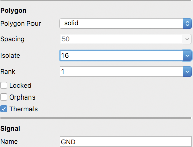
Figure 4-16: Changing the name of the polygon to GND will result in all of the ground connections contiguous with the polygon being merged into a plane. The Isolate field will make sure that there is at least that much clearance between the ground plane and any traces (16 mils in this case).
Drawing a Custom StopMask Layer
In Chapter 2 you saw how to import bitmap images into a custom silkscreen layer. You can also import bitmaps into other layers, like the top or bottom copper or stopmask layers. What is nice about drawing into the stopmask layer is that any copper left exposed by the stopmask will be plated in nickel or gold (depending on your manufacturing process), effectively giving you a second way of marking or decorating your boards. Use the bitmaps included in the GitHub repository to create the graphic shown in Figure 4-17.
Your manufacturer will usually remove any place that the silkscreen ink overlaps with pads or stopmask, so you need to account for this in generating the bitmap files (Figure 4-18).

Figure 4-17: Import a bitmap into the top stopmask layer (gray).

Figure 4-18: Import a bitmap into the silkscreen layer (blue shaded).
Going Further
Once you get your boards back, you have a couple of options for assembling surface-mount parts (see Figure 4-19). This design is easy enough to solder by hand with an iron or a hot-air rework gun. If you’re making a bunch of boards, you may want to go the solder paste route, in which case you’ll need a stencil to apply the paste before placing the parts and cooking them.
You can order a metal solder stencil from your PCB manufacturer for around $20. Metal requires a laser in the 1000W range, so most people can’t make one themselves. If you have access to a school or makerspace with a lower-power laser, you can make a perfectly fine stencil using Mylar or acetate. First export the tcream layer as a black-and-white bitmap; that’s the paste layer.
The trick to creating a Mylar or acetate stencil is to use the etching settings on your laser, rather than cutting the outlines as vectors. If you’re using a 35W laser, try a speed setting of 15 and a power setting of 40 at 1200dpi (your settings may vary!).

Figure 4-19: A metal stencil (left) or DIY Mylar (right)