

Architecture and technical overview
This chapter describes the overall system architecture for the IBM Power System E980 (9080-M9S) server. The bandwidths that are provided throughout the section are theoretical maximums that are used for reference.
The speeds that are shown are at an individual component level. Multiple components and application implementation are key to achieving the best performance.
Always do performance sizing at the application workload environment level and evaluate performance by using real-world performance measurements and production workloads.
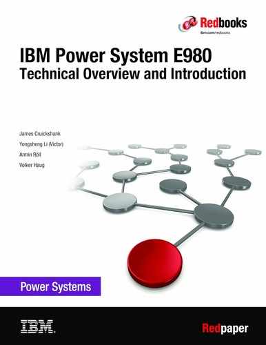
Figure 2-1 shows the logical system architecture of the Power E980 server.

Figure 2-1 Power E980 logical system diagram
Figure 2-2 shows the symmetric multiprocessing (SMP) connections between nodes for 2-, 3-, and 4-drawer configurations.

Figure 2-2 Symmetric multiprocessing cabling
2.1 The IBM POWER9 processor
This section introduces the latest processor in the IBM Power Systems product family, and describes its main characteristics and features in general.
2.1.1 POWER9 processor overview
The POWER9 processors are single-chip modules (SCMs) manufactured on the IBM 14-nm FinFET Silicon-On-Insulator (SOI) architecture. Each module is 68.5 mm x 68.5 mm and contains 8 billion transistors.
As shown in Figure 2-3, the chip contains 12 cores, two memory controllers, Peripheral Component Interconnect Express (PCIe) Gen4 I/O controllers, and an interconnection system that connects all components within the chip at 7 TBps. Each core has 512 KB of level 2 cache, and 10 MB of level 3 embedded DRAM (eDRAM) cache. The interconnect also extends through module and system board technology to other POWER9 processors in addition to memory and various I/O devices.

Figure 2-3 The POWER9 processor chip
The Power E980 server uses memory buffer chips to interface between the POWER9 processor and the DDR3 or DDR4 memory. Each buffer chip also includes an L4 cache to reduce the latency of local memory accesses.
The POWER9 chip provides an embedded algorithm for the following features:
•External Interrupt Virtualization Engine. Reduces the code impact/path length and improves performance compared to the previous architecture.
•Compression and decompression.
•PCIe Gen4 support.
•Two memory controllers that support buffered connection to DDR3 or DDR4 memory.
•Cryptography: Advanced encryption standard (AES) engine.
•Random number generator (RNG).
•Secure Hash Algorithm (SHA) engine: SHA-1, SHA-256, and SHA-512, and Message Digest 5 (MD5)
•IBM Data Mover Tool
Table 2-1 provides a summary of the POWER9 processor-based technology.
|
Note: The total values represent the maximum of 12 cores for the POWER9 processor-based architecture. The Power E980 server has options for 24, 32, 40, 44, and 48 cores per node.
|
Table 2-1 Summary of the POWER9 processor-based technology
|
Technology
|
POWER9 processor
|
|
Die size
|
68.5 mm × 68.5 mm
|
|
Fabrication technology
|
•14-nm lithography
•Copper interconnect
•SOI
•eDRAM
|
|
Maximum processor cores
|
12
|
|
Maximum execution threads core/module
|
8/96
|
|
Maximum L2 cache core/module
|
512 KB/6 MB
|
|
Maximum On-chip L3 cache core/module
|
10 MB/120 MB
|
|
Number of transistors
|
8 billion
|
|
Compatibility
|
With prior generation of POWER processor
|
2.1.2 POWER9 processor core
The POWER9 processor core is a 64-bit implementation of the IBM Power Instruction Set Architecture (ISA) Version 3.0, and has the following features:
•Multi-threaded design, which is capable of up to eight-way simultaneous multithreading (SMT)
•64 KB, eight-way set-associative L1 instruction cache
•64 KB, eight-way set-associative L1 data cache
•Enhanced prefetch, with instruction speculation awareness and data prefetch depth awareness
•Enhanced branch prediction that uses both local and global prediction tables with a selector table to choose the best predictor
•Improved out-of-order execution
•Two symmetric fixed-point execution units
•Two symmetric load/store units and two load units, all four of which can also run simple fixed-point instructions
•An integrated, multi-pipeline vector-scalar floating point unit for running both scalar and SIMD-type instructions, including the Vector Multimedia eXtension (VMX) instruction set and the improved Vector Scalar eXtension (VSX) instruction set, which is capable of up to 16 floating point operations per cycle (eight double precision or 16 single precision)
•In-core AES encryption capability
•Hardware data prefetching with 16 independent data streams and software control
•Hardware decimal floating point (DFP) capability
For more information about Power ISA Version 3.0, see OpenPOWER: IBM Power ISA Version 3.0B.
Figure 2-4 shows a picture of the POWER9 core, with some of the functional units highlighted.

Figure 2-4 POWER9 processor chip
2.1.3 Simultaneous multithreading
POWER9 processor advancements in multi-core and multi-thread scaling are remarkable. A significant performance opportunity comes from parallelizing workloads to enable the full potential of the microprocessor, and the large memory bandwidth. Application scaling is influenced by both multi-core and multi-thread technology.
SMT enables a single physical processor core to simultaneously dispatch instructions from more than one hardware thread context. With SMT, each POWER9 core can present eight hardware threads. Because there are multiple hardware threads per physical processor core, more instructions can run at the same time.
SMT is primarily beneficial in commercial environments where the speed of an individual transaction is not as critical as the total number of transactions that are performed. SMT typically increases the throughput of workloads with large or frequently changing working sets, such as database servers and web servers.
Table 2-2 shows a comparison between the different POWER processors in terms of SMT capabilities that are supported by each processor architecture.
Table 2-2 SMT levels that are supported by POWER processors
|
Technology
|
Cores/system
|
Maximum SMT mode
|
Maximum hardware threads per partition
|
|
IBM POWER4
|
32
|
Single thread
|
32
|
|
IBM POWER5
|
64
|
SMT2
|
128
|
|
IBM POWER6
|
64
|
SMT2
|
128
|
|
IBM POWER7
|
256
|
SMT4
|
1024
|
|
IBM POWER8
|
192
|
SMT8
|
1536
|
|
IBM POWER9
|
192
|
SMT8
|
1536
|
2.1.4 POWER9 compatibility modes
The POWER9 processor can run in compatibility modes for previous POWER processor generations. This enables older operating systems (OSes) to run on POWER9 systems. Compatibility modes also allow for LPM from systems based on previous generations of POWER processors. The POWER9 processor can run in the following compatibility modes:
•POWER7
•POWER8
•POWER9 Base
2.1.5 Processor feature codes
Each system enclosure in a Power E980 server has four sockets for processor modules. All sockets must be populated with a matching processor module. In servers with multiple system enclosures, all sockets on all enclosures must be populated with matching processor modules.
Table 2-3 shows the processor feature codes that are available for the Power E980 server.
Table 2-3 Power E980 processor features
|
Feature code
|
CCIN
|
Description
|
|
EFB1
|
5C35
|
CBU for Power Enterprise Systems typical 3.9 to 4.0 GHz (max), 32-core POWER9 processor
|
|
EFB2
|
5C36
|
CBU for Power Enterprise Systems typical 3.7 to 3.9 GHz (max), 40-core POWER9 processor
|
|
EFB3
|
5C39
|
CBU for Power Enterprise Systems typical 3.55 to 3.9 GHz (max), 48-core POWER9 processor
|
|
EFB4
|
5C46
|
CBU for Power Enterprise Systems typical 3.58 to 3.9 GHz (max), 44-core POWER9 processor
|
|
EFBZ
|
5C33
|
CBU for Power Enterprise Systems typical 3.58 to 3.9 GHz (max), 24-core POWER9 processor
|
|
EFP0
|
5C33
|
24-core (4x6) typical 3.58 to 3.9 GHz (max) POWER9 Processor
|
|
EFP1
|
5C35
|
32-core (4x8) typical 3.9 to 4.0 GHz (max) POWER9 Processor
|
|
EFP2
|
5C36
|
40-core (4x10) typical 3.7 to 3.9 GHz (max) POWER9 Processor
|
|
EFP3
|
5C39
|
48-core (4x12) typical 3.55 to 3.9 GHz (max) POWER9 Processor
|
|
EFP4
|
5C46
|
44-core (4x11) typical 3.58 to 3.9 GHz (max) POWER9 Processor
|
|
EHC6
|
5C36
|
Solution Edition for Healthcare typical 3.7 to 3.9 GHZ, 40-core POWER9 Processor
|
Processors in the Power E980 system support Capacity on Demand (CoD). For more information about CoD, see 2.3, “Capacity on Demand” on page 78.
Processor-specific CoD features are shown in Table 2-4.
Table 2-4 Processor activation feature codes
|
Processor feature
|
Static activation feature
|
Mobile enabled activation feature
|
Static activation for Linux feature
|
|
EFP0 (3.58 - 3.9 GHz 24-core)
|
EFPQ
|
EFPR
|
ELBS
|
|
EFP1 (3.9 - 4.0 GHz 32-core)
|
EFPA
|
EFPE
|
ELBK
|
|
EFP2 (3.7 - 3.9 GHz 40-core)
|
EFPB
|
EFPF
|
ELBL
|
|
EFP3 (3.55 - 3.9 GHz 48-core)
|
EFPC
|
EFPG
|
ELBM
|
|
EFP4 (3.58 - 3.9 GHz 44-core)
|
EFP9
|
EFPN
|
ELBQ
|
CoD features that are independent of the processor feature are shown in Table 2-5.
Table 2-5 Processor-independent activation features
|
Feature code
|
Feature description
|
|
EF2R
|
Single 5250 Enterprise Enablement
|
|
EF30
|
Full 5250 Enterprise Enablement
|
|
EFPD
|
Mobile processor activation for M9S/80H
|
|
EFPH
|
Mobile processor activation for M9S/80H (Upgrade from POWER7)
|
|
EP2W
|
Mobile Processor activation M9S/80H (Upgrade from POWER8)
|
|
EP9T
|
90 Days Elastic CoD Processor Core Enablement
|
|
MMC1
|
Elastic CoD Processor Day for IBM i
|
|
MMCX
|
Elastic CoD Processor Day for AIX and Linux
|
2.1.6 Memory access
One POWER9 processor module of a Power E980 high-end system provides two integrated memory controllers to facilitate access to the main memory of the system. One memory controller drives four differential memory interface (DMI) channels with a maximum signaling rate of 9.6 GHz. This yields a peak memory bandwidth of up to 28.8 GBps per memory channel or 230.4 GBps per processor module. Every DMI channel connects to one dedicated memory buffer chip. Each memory buffer chip provides four DDR4 memory ports running at 1,600 MHz signal rate and one 16 MB L4 cache. A single memory buffer chip is mounted with the associated DRAM chips on one circuit board, which is referred to as custom DIMM (CDIMM) module.
With a new system order, the DDR4 technology-based CDIMMs are available with 32 GB, 64 GB, 128 GB, 256 GB, and 512 GB capacity. Also, the POWER9 memory channels support the same electrical signaling, transport layer characteristics, and high-level, neutral read/write protocol as the POWER8 counterparts on Power E870, Power E870C, Power E880, and Power E880C servers. This enables the option to reuse DDR3 and DDR4 CDIMMs when transferred as part of a model upgrade from the named POWER8 high-end servers to a Power E980 system.
The maximum supported memory capacity per processor module is 4 TB, which requires the use of 512 GB CDIMMs in all eight available CDIMM slots of a module. A maximum of 16 TB of main memory can be provided by the four processor modules that are available in one system node. A 4-node Power E980 system makes up to 64 TB of system memory accessible to configured logical partitions (LPARs).
Figure 2-5 shows the POWER9 hierarchical memory subsystem of a Power E980 system.

Figure 2-5 POWER9 hierarchical memory subsystem that uses memory buffers
For more information about the CDIMM technology, memory placement rules, memory bandwidth, and other topics that are related to the memory subsystem of the Power E980 server, see 2.2, “Memory subsystem” on page 68.
2.1.7 On-chip L3 cache innovation and intelligent caching
Similar to the POWER8 processor, the POWER9 processor uses a breakthrough in material engineering and microprocessor fabrication to implement the L3 cache in eDRAM technology and place it on the processor die. The L3 cache is critical to a balanced design, as is the ability to provide good signaling between the L3 cache and other elements of the hierarchy, such as the L2 cache or SMP interconnect.
Like the POWER8 processor, the POWER9 processor supports the same L3 non-uniform cache access (NUCA) architecture that provides mechanisms to distribute and share cache footprints across the chip. The on-chip L3 cache is organized into separate areas with differing latency characteristics. Each processor core is associated with a fast 10 MB local region of L3 cache (FLR-L3), but also has access to other L3 cache regions as a shared L3 cache. Additionally, each core can negotiate to use the FLR-L3 cache that is associated with another core, depending on the reference patterns. Data can also be cloned and stored in more than one core’s FLR-L3 cache, again depending on the reference patterns.
This intelligent cache management enables the POWER9 processor to optimize the access to L3 cache lines and minimize overall cache latencies. Regarding the POWER8 L3 implementation, the POWER9 L3 introduces an enhanced replacement algorithm with data type and reuse awareness that uses information from the core and L2 cache to manage cache replacement states. The L3 cache supports an array of prefetch requests from the core, including both instruction and data, and for different levels of urgency. Prefetch requests for POWER9 cache include more information exchange between the core, cache, and the memory controller to manage memory bandwidth and to mitigate the prefetch-based cache pollution.
The following list provides an overview of the features that are offered by the POWER9 L3 cache:
•Private 10 MB L3.0 cache/shared L3.1:
– Victim cache for local L2 cache (L3.0)
– Victim cache for other on-chip L3 caches (L3.1)
•20-way set associative.
•128-byte cache lines with 64-byte sector support.
•Ten EDRAM banks (interleaved for access overlapping).
•64-byte wide data bus to L2 for reads.
•64-byte wide data bus from L2 for L2 castouts.
•Eighty 1 Mb EDRAM macros that are configured in 10 banks, with each bank having a 64-byte wide data bus.
•All cache accesses have the same latency.
•20-way directory that is organized as four banks, with up to four reads or two reads and two writes every two processor clock cycles to differing banks.
The L3 cache architecture of the 12-core POWER9 processor is identical to the 24-core POWER9 implementation. For more information about the L3 cache technology, see POWER9 Processor User’s Manual.
For more information about the L3 cache in the context of the POWER9 core architecture, see H. Le, et al., IBM POWER9 processor core, IBM Journal of Research & Development Volume 62 Number 4/5, July/September 2018, which you can search for at IBM Journal of Research & Development.
2.1.8 Hardware transactional memory
Transactional memory is an alternative to lock-based synchronization. It attempts to simplify parallel programming by grouping read and write operations and running them like a single operation. Transactional memory is like database transactions where all shared memory accesses and their effects are either committed or discarded as a group. All threads can enter the critical region simultaneously. If there are conflicts in accessing the shared memory data, threads try accessing the shared memory data again or are stopped without updating the shared memory data. Therefore, transactional memory is also called a lock-free synchronization. Transactional memory can be a competitive alternative to lock-based synchronization.
Transactional memory provides a programming model that makes parallel programming easier. A programmer delimits regions of code that access shared data, and the hardware runs these regions atomically and in isolation, buffering the results of individual instructions and retrying execution if isolation is violated. Generally, transactional memory enables programs to use a programming style that is close to coarse-grained locking to achieve performance that is close to fine-grained locking.
Most implementations of transactional memory are based on software. The POWER9 processor-based systems provide a hardware-based implementation of transactional memory that is more efficient than the software implementations and requires no interaction with the processor core, therefore enabling the system to operate at maximum performance.
2.1.9 POWER9 accelerator processor interfaces
The POWER9 processor supports three dedicated interfaces and protocols to attach advanced accelerator and future memory technologies:
•Coherent Accelerator Processor Interface (CAPI)
•Open Coherent Accelerator Processor Interface (OpenCAPI)
•NVIDIA NVLink
The CAPI protocol uses the PCIe Gen4 bus, which is natively supported on the POWER9 processor die. CAPI-capable accelerators are implemented as adapters that are placed in a CAPI-enabled PCIe Gen3 or Gen4 slot. The maximum bandwidth of a CAPI accelerator is limited by the PCIe bandwidth, which is 64 GBps for a x16 PCIe Gen4 adapter slot in a POWER9 processor-based system.
All eight x16 PCIe Gen4 slots in a Power E980 system node are enabled for CAPI support, which yields a maximum of 32 CAPI-attached accelerators per 4-node system. The CAPI protocol has been developed and standardized since 2013 by the OpenPOWER Foundation. For more information about the CAPI protocol, see the OpenPOWER Foundation.
On Power E980 systems, OpenCAPI-attached accelerators and devices and NVLink graphics processing unit (GPU) connections are supported by two buses per POWER9 processor. They are using the same interconnect technology that facilitates the SMP communication between Power E980 nodes and provides a combined transfer capacity of 48 lanes running with a signaling rate of 25.78 Gbps. Each system node has four interconnect buses, which are referred to as O-buses O0, O1, O2, and O3, which are designed to support the SMP, OpenCAPI, or NVLink protocol.
On Power E980 system nodes, the buses are configured to support the following protocols:
•O0: SMP, NVLink, or OpenCAPI
•O1: SMP only
•O2: SMP only
•O3: SMP, NVLink, or OpenCAPI
The OpenCAPI technology is developed and standardized by the OpenCAPI Consortium. For more information about the consortium’s mission and the OpenCAPI protocol specification, see OpenCAPI Consortium.
The NVLink 2.0 protocol is natively supported by dedicated logic on the POWER9 processor die. By using it, you can coherently attach NVIDIA GPUs through a maximum of two O-buses per processor. Each NVLink O-bus is composed of two bricks, and each brick provides eight data lanes in NVLink mode running at 25 Gbps signaling rate. The maximum bandwidth of one O-bus that is used to attach a NVLink GPU is 103.12 GBps, as calculated by the following formula:
Two bricks x 8 lanes x 25.78 Gbps x 2 full duplex = 103.12 GBps
The NVLink technology is developed by the NVIDIA Corporation. For more information about the NVLink protocol, see NVIDIA NVLink.
|
Note: The Power E980 system supports the OpenCAPI and the NVLink protocol, but at the time of writing OpenCAPI-attached accelerators these technologies are included for future reference only.
|
Coherent Accelerator Processor Interface 2.0
IBM CAPI 1.0, along with the related coherent accelerator interface architecture (CAIA), was introduced with POWER8 in 2014. By using CAPI 1.0, you may attach special processing devices or accelerators to the POWER8 processor bus through the native PCIe Gen3 interface. The attached devices exhibit the form factor of a standard PCIe adapter and typically use field programmable gate arrays (FPGAs) or application-specific integrated circuits (ASICs) to provide a specific function with significantly enhanced performance. In the CAPI paradigm, the specific algorithm for acceleration is contained in a unit on the FPGA or ASIC and is called the accelerator function unit (AFU).
One of the key benefits of CAPI is that the devices gain coherent shared memory access with the processors in the server and share full virtual address translation with these processors by using the standard PCIe interconnect logic. In CAPI 1.0, the address translation logic of the attached devices or accelerators is implemented as POWER Service Layer (PSL) on the FPGA or ASIC. To ensure cache coherency, the PSL exchanges the relevant address information with the coherent accelerator processor proxy (CAPP) unit that is on the POWER8 processor chip.
Applications can have customized functions in FPGAs or ASICs and queue work requests directly into shared memory queues to the accelerator logic. Applications can also have customized functions by using the same effective addresses that they use for any threads running on a host processor. From a practical perspective, CAPI enables a specialized hardware accelerator to be seen as a dedicated processor (hollow core) in the system with access to the main system memory and coherent communication with other processors in the system.
CAPI 2.0 was introduced with the POWER9 processor-based technology and represents the next step in the evolutionary development to enhance the architecture and the protocol for the attachment of accelerators. CAPI 2.0 uses the standard PCIe Gen4 interface of the POWER9 processor, which provides twice the bandwidth compared to the previous PCIe Gen3 interconnect generation.
A key difference between CAPI 1.0 and CAPI 2.0 relies on the introduction of the Nest Memory Management Unit (NMMU) with POWER9. The NMMU replaces the address translation and page fault logic inside the PSL. CAPI 2.0 on POWER9 still requires a PSL to control the PCIe bus, provide the memory mapped I/O (MMIO) support, and generate AFU-specific interrupts. However, by taking the address translation and page fault logic out of the POWER9 PSL, it has become a “lighter” version of the POWER8 PSL, which potentially reduces the complexity of accelerator development.
Figure 2-6 shows a block diagram of the CAPI 2.0 POWER9 hardware architecture.

Figure 2-6 CAPI 2.0 POWER9 system block diagram
The POWER9 processor modules of the Power E980 server provide fault handling for the PSL.
The benefits of using CAPI include the ability to access shared memory blocks directly from the accelerator, perform memory transfers directly between the accelerator and processor cache, and reduce the code path length between the adapter and the processors. This reduction in the code path length might occur because the adapter is not operating as a traditional I/O device, and there is no device driver layer to perform processing. CAPI also presents a simpler programming model.
Figure 2-7 shows a comparison of the traditional model, where the accelerator must go through the processor to access memory with CAPI.

Figure 2-7 CAPI accelerator that is attached to the POWER9 processor
As mentioned before with CAPI 1.0 on POWER8, the PSL on the accelerator adapter provides address translation and system memory cache for the accelerator functions. The custom processors on the adapter board, consisting of an FPGA or an ASIC, use this layer to access shared memory regions and cache areas as though they were a processor in the system. This ability enhances the performance of the data access for the device and simplifies the programming effort to use the device. Instead of treating the hardware accelerator as an I/O device, it is treated as a processor, which eliminates the requirement of a device driver to perform communication. It also eliminates the need for direct memory access (DMA) that requires system calls to the OS kernel. By removing these layers, the data transfer operation requires fewer clock cycles in the processor, improving the I/O performance.
With CAPI 2.0 on POWER9, the address translation and page fault logic are moved to the native NMMU on the POWER9 processor module, but because the accelerator has direct access to this functional unit, the benefit of reduced path length in the programming model stays the same, and the cache coherency control of the unified address space is significantly enhanced.
The implementation of CAPI on the POWER9 processor enables hardware companies to develop solutions for specific application demands. Companies use the performance of the POWER9 processor for general applications and the custom acceleration of specific functions by using a hardware accelerator with a simplified programming model and efficient communication with the processor and memory resources.
Open Coherent Accelerator Processor Interface
In October 2016, the companies AMD, Google, IBM, Mellanox Technologies, and Micron formed the OpenCAPI not-for-profit organization to create an open, coherent, and high-performance bus interface that is based on a new bus standard that is called Open Coherent Accelerator Processor Interface (OpenCAPI), and to grow the infrastructure that uses this interface. This initiative is driven by the emerging accelerated computing and advanced memory/storage solutions that introduced significant system bottlenecks in today’s current open bus protocols, which requires a technical solution that is openly available.
Two major technology trends heavily impact the industry currently:
•Hardware acceleration becomes commonplace as microprocessor technology and design continues to deliver far less than the historical rate of cost/performance improvement per generation.
•New advanced memory technologies change the economics of computing.
Existing system interfaces are insufficient to address these disruptive forces. Traditional I/O architecture results in high processor impact when applications communicate with I/O or accelerator devices at the necessary performance levels. Also, they cannot integrate multiple memory technologies with different access methods and performance attributes.
These challenges are addressed by the OpenCAPI architecture in a way that allows full industry participation. Embracing an open architecture is fundamental to establish sufficient volume base to lower costs and ensure the support of a broad infrastructure of software products and attached devices.
OpenCAPI is an open interface architecture that allows any microprocessor to attach to the following items:
•Coherent user-level accelerators and I/O devices
•Advanced memories accessible through read/write or user-level DMA semantics
OpenCAPI is neutral to processor architecture and exhibits the following key attributes:
•High-bandwidth, low latency interface that is optimized to enable streamlined implementations of attached devices.
•A 25 Gbps signaling and protocol that enables a low latency interface on processors and attached devices.
•Complexities of coherence and virtual addressing that is implemented on a host microprocessor to simplify attached devices and facilitate interoperability across multiple CPU architectures.
•Attached devices operate natively within an application’s user space and coherently with processors, enabling attached devices to fully participate in applications without kernel involvement/impact.
•Supports a wide range of use cases and access semantics:
– Hardware accelerators
– High-performance I/O devices
– Advanced memories
2.1.10 Power and performance management
POWER9 processor-based scale-out and scale-up servers implement Workload Optimized Frequency (WOF) as a new feature of the power management EnergyScale technology. With POWER9 EnergyScale, the POWER8 dynamic power saver (DPS) modes that either favor lower power consumption (DPS) or favor performance (dynamic power saver favors performance (DPS-FP)) are replaced by two new power saver modes:
•Dynamic performance mode (DPM)
•Maximum performance mode (MPM)
Every POWER9 processor-based scale-out or scale-up system has either DPM or MPM enabled by default. Both modes dynamically adjust processor frequency to maximize performance and enable a much higher processor frequency range in comparison to POWER8 servers. Each of the new power saver modes delivers consistent system performance without any variation if the nominal operating environment limits are met.
For POWER9 processor-based systems that are under control of the PowerVM hypervisor, the DPM and MPM are a system-wide configuration setting, but each processor module frequency is optimized separately.
Several factors determine the maximum frequency that a processor module can run at:
•Processor utilization: Lighter workloads run at higher frequencies.
•Number of active cores: Fewer active cores run at higher frequencies.
•Environmental conditions: At lower ambient temperatures, cores are enabled to run at higher frequencies.
The new power saver modes are defined as follows:
Dynamic performance mode (DPM)
In DPM, the workload is run at the highest frequency possible if the nominal power consumption limit of the processor modules is not exceeded. The frequency of the processor modules is always at the nominal frequency of the POWER9 processor-based system or above the nominal frequency up to the upper limit of the DPM frequency range. This DPM typical frequency range (DTFR) is published as part of the system specifications of a particular POWER9 system if it is running by default in the DPM.
In DPM, the workload is run at the highest frequency possible if the nominal power consumption limit of the processor modules is not exceeded. The frequency of the processor modules is always at the nominal frequency of the POWER9 processor-based system or above the nominal frequency up to the upper limit of the DPM frequency range. This DPM typical frequency range (DTFR) is published as part of the system specifications of a particular POWER9 system if it is running by default in the DPM.
The system performance is deterministic within the allowed operating environmental limits and as such does not depend on the ambient temperature if the temperature stays within the supported range. The idle power saver (IPS) function can be enabled or disabled. If IPS is enabled and all cores in a processor module are idle for hundreds of milliseconds, the frequency of the cores in the respective module drop to the predefined power save frequency.
Maximum performance mode (MPM)
In MPM, the workload is run at the highest frequency possible, but unlike in the DPM the processor module may operate at a higher power consumption level. The higher power draw enables the processor modules to run in an MPM typical frequency range (MTFR), where the lower limit is well above the nominal frequency and the upper limit is given by the system’s maximum frequency.
In MPM, the workload is run at the highest frequency possible, but unlike in the DPM the processor module may operate at a higher power consumption level. The higher power draw enables the processor modules to run in an MPM typical frequency range (MTFR), where the lower limit is well above the nominal frequency and the upper limit is given by the system’s maximum frequency.
The MTFR is published as part of the system specifications of a particular POWER9 system if it is running by default in MPM. The higher power draw potentially increase the fan speed of the respective system node to meet the higher cooling requirements, which in turn cause a higher noise emission level of up to 15 decibels.
The processor frequency typically stays within the limits that are set by the MTFR, but may be lowered to frequencies between the MTFR lower limit and the nominal frequency at high ambient temperatures above 22 °C (71.1 °F). If the data center ambient environment is less than 22 °C, the frequency in MPM consistently is in the upper range of the MTFR (roughly 10% to 20% better than nominal). At lower ambient temperatures (below 25 °C), MPM mode also provides deterministic performance. As the ambient temperature increases above 25 °C, determinism can no longer be guaranteed.
The IPS function can be enabled or disabled. If IPS is enabled, the frequency is dropped to the static power saver level if the entire system meets the configured idle conditions.
Figure 2-8 shows the frequency ranges for the POWER9 static nominal mode (all modes disabled), the DPM, and the MPM. The frequency adjustments for different workload characteristic, ambient conditions, and idle states are also indicated.

Figure 2-8 POWER9 power management modes and related frequency ranges
Table 2-6 shows the static nominal and the static power saver mode frequencies, and the frequency ranges of the DPM and the MPM for all four processor module types that are available for the Power E980 system.
Table 2-6 Characteristic frequencies and frequency ranges for Power E980 server
|
Feature code
|
Cores per single-chip module
|
Static nominal frequency
[GHz]
|
Static power saver mode frequency
[GHz]
|
Dynamic performance mode frequency range
[GHz]
|
Maximum performance mode frequency range
[GHz]
|
|
EFP1
|
8
|
3.4
|
2.75
|
3.4 - 4.0
|
3.9 - 4.0
|
|
EFP2
|
10
|
3.15
|
2.75
|
3.15 - 3.9
|
3.7 - 3.9
|
|
EFP3
|
12
|
2.90
|
2.75
|
2.9 - 3.9
|
3.55 - 3.9
|
|
EFP4
|
11
|
3.00
|
2.75
|
3.0 - 3.9
|
3.58 - 3.9
|
Figure 2-9 shows the POWER9 processor frequency as a function of power management mode and system utilization.

Figure 2-9 POWER9 processor frequency as a function of power management mode and system load
The default performance mode depends on the POWER9 processor-based server model. For Power E980 systems, the MPM is enabled by default.
The controls for all power saver modes are available on the Advanced System Management Interface (ASMI) and can be dynamically modified. This includes to enable or to disable the IPS function and change the EnergyScale tunable parameters. A system administrator may also use the Hardware Management Console (HMC) to disable all power saver modes or to enable one of the three available power and performance modes: static power saver mode, DPM, or MPM.
Figure 2-10 shows the ASMI menu for Power and Performance Mode Setup on a Power E980 server.

Figure 2-10 Power E980 ASMI menu for power and performance mode setup
For more information about the POWER9 EnergyScale technology, see POWER9 EnergyScale Introduction.
2.1.11 Comparison of the POWER9, POWER8, and POWER7+ processors
The Power E980 and the Power E950 Enterprise systems use exclusively processor modules with 12 cores that are SMT8 capable. These scale-up processor modules are performance optimized and for the usage in scale-up multi-sockets systems.
The Power S914, Power S922, Power H922, Power L922, Power S924, and Power H924 systems can be ordered with processor modules with 12-cores that are SMT8 capable. These scale-out processor modules are performance optimized in scale-out two socket systems.
The Power LC921, Power LC922, and Power AC922 systems use 24-core modules and are SMT4 capable. These scale-out processor modules are Linux Ecosystem optimized in scale-out two socket systems.
Table 2-7 shows key features and characteristics in comparison between the POWER9 scale-up, POWER9 scale-out, POWER8, and POWER7+ processor implementations.
Table 2-7 Comparison of technology for the POWER9 processor and prior processor generations
|
Characteristics
|
POWER9 performance optimized
|
POWER9 Linux Ecosystems optimized
|
POWER8
|
POWER7+
|
|
Technology
|
14 nm
|
14 nm
|
22 nm
|
32 nm
|
|
Die size
|
68.5 mm x 68.5 mm
|
68.5 mm x 68.5 mm
|
649 mm2
|
567 mm2
|
|
Number of transistors
|
8 billion
|
8 billion
|
4.2 billion
|
2.1 billion
|
|
Maximum cores
|
12
|
24
|
12
|
8
|
|
Maximum SMT threads per core
|
Eight threads
|
Four threads
|
Eight threads
|
Four threads
|
|
Maximum frequency
|
3.9 - 4.0 GHz
|
3.8 - 4.0 GHz
|
4.15 GHz
|
4.4 GHz
|
|
L2 Cache
|
512 KB per core
|
512 KB per core
|
512 KB per core
|
256 KB per core
|
|
L3 Cache
|
10 MB of L3 cache per core with each core having access to the full 120 MB of L3 cache, on-chip eDRAM
|
10 MB of L3 cache that is shared by two cores with each core having access to the full 120 MB of L3 cache, on-chip eDRAM
|
8 MB of L3 cache per core with each core having access to the full 96 MB of L3 cache, on-chip eDRAM
|
10 MB of L3 cache per core with each core having access to the full 80 MB of L3 cache, on-chip eDRAM
|
|
Memory support
|
DDR4 and DDR31
|
DDR4
|
DDR3 and DDR4
|
DDR3
|
|
I/O bus
|
PCIe Gen4
|
PCIe Gen4
|
PCIe Gen3
|
GX++
|
1 Only DDR3 memory CDIMMs, which are transferred in the context of a model upgrade from Power E870, Power E870C, Power E880, or Power E880C systems to a Power E980 server, are supported.
2.2 Memory subsystem
The Power E980 server uses the same CDIMM technology that is found in POWER8 processor-based systems. Each system node has 32 CDIMM slots that can support 16 GB, 32 GB, 64 GB, 128 GB, 256 GB, and 512 GB CDIMMs running at a speed of 1600 MHz.
The Power E980 system supports both DDR3 and DDR4 versions of the CDIMM. Mixing of DDR3 and DDR4 CDIMMs is not supported in the same system node, but DDR3 CDIMMs in one system node and DDR4 CDIMMs in another system node is supported in the same Power E980 server.
New orders of Power E980 servers can be configured only with DDR4 CDIMMs of 32 GB, 64 GB, 128 GB, 256 GB, and 512 GB capacities.
To provide significant investment protection, the 16 GB, 32 GB, 64 GB, 128 GB, 256 GB DDR4 CDIMMs and the 16 GB, 32 GB, 64 GB, 128 GB, DDR3 CDIMMs of the Power E870, Power E870C, Power E880, and Power E880C servers are supported in the context of model upgrades to Power E980 systems.
The memory subsystem of the Power E980 server enables a maximum system memory of 16 TB per system node. A 4-node system can support up to 64 TB of system memory.
The memory of Power E980 systems is CoD-capable, allowing for the purchase of extra physical memory capacity that can then be dynamically activated when needed. 50% of the installed memory capacity must be active.
The Power E980 server supports an optional feature called Active Memory Expansion (AME) (#EM89). This allows the effective maximum memory capacity to be much larger than the true physical memory. This feature uses a dedicated coprocessor on the POWER9 processor to compress memory pages as they are written to and decompress them as they are read from memory. This can deliver memory expansion of up to 125%, depending on the workload type and its memory usage.
2.2.1 Custom DIMM
CDIMMs are innovative memory DIMMs that house industry-standard DRAM memory chips and a set of components that allows for higher bandwidth, lower latency communications, and increased availability. These components include:
•Memory Scheduler
•Memory Management (reliability, availability, and serviceability (RAS) decisions and energy management)
•Memory Buffer
By adopting this architecture for the memory DIMMs, several decisions and processes regarding memory optimizations are run internally in the CDIMM, which saves bandwidth and allows for faster processor-to-memory communications. This also allows for a more robust RAS. For more information, see Chapter 4, “Reliability, availability, serviceability, and manageability” on page 125.
Depending on the memory capacity, the CDIMMs are manufactured in a Tall CDIMM or a Short CDIMM form factor. The 16 GB, 32 GB, and 64 GB CDIMMs are Short CDIMMs and the 128 GB, 256 GB, and 512 GB CDIMMs are the Tall CDIMMs. Each design is composed of a varying number of 4 Gb or 8 Gb SDRAM chips depending on the total capacity of the CDIMM. The large capacity 256 GB and 512 GB CDIMMs are based on two-high (2H) and four-high (4H) 3D-stacked (3DS) DRAM technology.
The CDIMM slots for the Power E980 server are Tall CDIMM slots. A filler is added to a Short CDIMM allowing it to properly latch into the same physical location of a Tall CDIMM and ensure proper airflow and ease of handling. Tall CDIMMs slots allow for larger DIMM sizes and potentially a more seamless adoption of future technologies.
A detailed diagram of the CDIMMs that are available for the Power E980 server is shown in Figure 2-11.

Figure 2-11 Short CDIMM and Tall CDIMM details
The memory buffer is a L4 cache and is built on eDRAM technology (same as the L3 cache), which has a lower latency than regular SRAM. Each CDIMM has 16 MB of L4 cache, and a fully populated Power E980 server has 2 GB of L4 cache. The L4 cache performs several functions that have direct impact on performance and bring a series of benefits to the Power E980 server:
•Reduces energy consumption by reducing the number of memory requests.
•Increases memory write performance by acting as a cache and by grouping several random writes into larger transactions.
•Partial write operations that target the same cache block are gathered within the L4 cache before being written to memory, becoming a single write operation.
•Reduces latency on memory access. Memory access for cached blocks has up to 55% lower latency than non-cached blocks.
2.2.2 Memory placement rules
For a Power E980 system, each memory FC provides four CDIMMs. Therefore, a maximum of eight memory FCs per system node are allowed to fill all 32 CDIMM slots. Populating all 128 CDIMM slots of a 4-node Power E980 server requires 32 memory features.
All the memory CDIMMs are capable of Capacity Upgrade on Demand (CUoD) and must have a minimum of 50% of their physical capacity activated. For example, the minimum installed memory for a Power E980 server is 512 GB, which requires a minimum of 256 GB memory activations.
For the Power E980 server, the following 1600 MHz DDR4 DRAM memory options are available when placing an initial order:
•128 GB (4 x 32 GB) (#EF20)
•256 GB (4 x 64 GB) (#EF21)
•512 GB (4 x 128 GB) (#EF22)
•1024 GB (4 x 256 GB) (#EF23)
•2048 GB (4 x 512 GB) (#EF24)
Each processor module has two memory controllers. These memory controllers must have at least a pair of CDIMMs that are attached to it. This set of mandatory four CDIMMs is called a memory quad.
A logical diagram of a POWER9 processor with its two memory quads attached to the memory controllers MC0 and MC1 is shown in Figure 2-12.

Figure 2-12 Logical diagram of a POWER9 processor and its two memory quads
The basic rules for memory placement are:
•Each FC designates a set of four physically identical CDIMMs, which is also referred to as a memory quad.
•One memory quad must be allocated to each installed processor module, which equals at least one memory FC per installed processor module.
•Of the 32 CDIMM slots in any system node, a minimum of 16 must be populated.
•A processor can have only four or eight CDIMMs that are attached to it.
•Not all CDIMMs connected to the same POWER9 processor module must be identical. You may configure two memory features of different CDIMM capacity per POWER9 processor module. However, for best performance results, the CDIMM size is ideally the same.
•At least 50% of the installed memory must be activated through memory activation features.
The suggested approach is to install memory evenly across all processors and across all system nodes in the server and the chosen CDIMM size is consistently equal for all memory slots. Balancing memory across the installed processors allows memory access in a consistent manner and typically results in the best possible performance for your configuration. You should account for any plans for future memory upgrades when you decide which memory feature size to use at the time of the initial system order.
A physical diagram with the location codes of the memory CDIMMs of a system node and heir grouping as memory quads is shown in Figure 2-13. Each system node has eight memory quads that are attached to the memory controllers MC0 and MC1 of the respective processor modules. The quads are identified by individually assigned color codes in Figure 2-13.

Figure 2-13 System node physical diagram with location codes for CDIMMs
Each Power E980 system node requires four memory quads to populate the required minimum of 16 CDIMM slots. The location codes of the slots for the memory quads 1 - 4 are shown in the following list. There is no specific ordering sequence that is implied because all four quads must be present in a valid configuration.
•Quad 1: P1-C46, P1-C47, P1-C52, and P1-C53 (slots connected to Processor P0)
•Quad 4: P1-C22, P1-C23, P1-C28, and P1-C29 (slots connected to Processor P1)
•Quad 2: P1-C38, P1-C39, P1-C44, and P1-C45 (slots connected to Processor P2)
•Quad 3: P1-C30, P1-C31, P1-C36, and P1-C37 (slots connected to Processor P3)
No mandatory plugging sequence must be adhered to for the population of any of the remaining open CDIMM slots. The locations codes for memory quads 5 - 8 are shown in the following list:
•Quad 5: P1-C48, P1-C49, P1-C50, and P1-C51 (slots connected to Processor P0)
•Quad 8: P1-C24, P1-C25, P1-C26, and P1-C27 (slots connected to Processor P1)
•Quad 6: P1-C40, P1-C41, P1-C42, and P1-C43 (slots connected to Processor P2)
•Quad 7: P1-C32, P1-C33, P1-C34, and P1-C35 (slots connected to Processor P3)
The numbering of quads 5 - 8 does not indicate any ordinal sequence, and any quad can be assigned to any processor module. The solution designer has the flexibility to assign the extra memory quads to any processor module if the minimum memory configuration is established. Furthermore, in multi-system node Power E980 servers, the solution designer can either fully populate one drawer and have the other drawers partially populated or have all the drawers symmetrically populated. For example, consider a 2-node Power E980 server with six extra quads of memory beyond the eight quads that are needed to fulfill the minimum memory configuration requirement. One option is to install four quads in one node and two quads in the other node. In an alternative configuration, both system nodes can be expanded by three quads each.
2.2.3 Memory activation
All the memory CDIMMs are capable of CUoD and must have a minimum of 50% of their physical capacity activated. For example, the minimum physical installed memory for the Power E980 system is 512 GB, which requires a minimum of 256 GB activated.
There are two activation types that can be used to accomplish this:
•Static memory activations: Memory activations that are exclusive for a single server.
•Mobile memory activations: Memory activations that can be moved from server to server in an IBM Power Enterprise Pool.
Both types of memory activations can be in the same system if at least 25% of the memory activations are static. This leads to a maximum of 75% of the memory activations as mobile.
Figure 2-14 shows an example of the minimum required activations for a system with 1 TB of installed memory.

Figure 2-14 Example of the minimum required activations for a system with 1 TB of installed memory
The granularity for static memory activation is 1 GB, and for mobile memory activation the granularity is 100 GB.
Specific FCs support memory activations for DDR3 or DDR4 memory CDIMMs that were transferred from Power E880 or Power E880C systems in the context of a model upgrade to a Power E980 server.
Table 2-8 lists the FCs that can be used to achieve the wanted number of activations.
Table 2-8 Static and mobile memory activation feature codes
|
Feature code
|
Feature description
|
Amount of memory
|
Type of activation
|
|
EMAT
|
1 GB Memory activation for M9S
|
1 GB
|
Static
|
|
EMAU
|
100 GB Memory activation for M9S
|
100 GB
|
Static
|
|
EMAV
|
100 GB Mobile memory activation for M9S
|
100 GB
|
Mobile
|
|
EFA1
|
1 GB Memory Activation (Upgrade from POWER8)
|
1 GB
|
Static
|
|
EFA2
|
100 GB Memory Activation (Upgrade from POWER8)
|
100 GB
|
Static
|
Static memory activations can be converted to mobile memory activations after system installation. To enable mobile memory activations, the systems must be part of an IBM Power Enterprise Pool and have #EB35 configured. For more information about IBM Power Enterprise Pools, see 2.3.5, “IBM Power Enterprise Pools and Mobile Capacity on Demand” on page 83.
2.2.4 Memory throughput
The Power E980 system can be configured with up to 16 processor modules. Each processor module drives eight memory channels at 9.6 GTps. Any transaction can provide 2-byte data read and 1-byte data write simultaneously. Memory bandwidth certainly varies with the workload, but the maximum theoretical memory bandwidth when using CDIMM at 1600 Mbps frequency in all eight slots of a processor module is approximately 230 GBps, which is calculated as follows:
9.6 GTps x 3 bytes/channel x 8 channels = 230.4 GBps
The total maximum theoretical memory bandwidth per Power E980 system node is 921.6 GBps, and the total maximum theoretical memory bandwidth per 4-node Power E980 system is 3686.4 GBps.
As data flows from main memory towards the execution units of the POWER9 processor, they pass through the 512 KB L2 and the 64 KB L1 cache. In many cases, the 10 MB L3 victim cache may also provide the data that is needed for the instruction execution.
Table 2-9 on page 75 shows the maximum cache bandwidth for a single core as defined by the width of the relevant channels and the related transaction rates on the Power E980 system.
Table 2-9 Power E980 single core architectural maximum cache bandwidth
|
Cache level of the POWER9 core
|
Power E980 cache bandwidth1
|
||||
|
3.58 - 3.9 GHz core (#EFP0)
[GBps]
|
3.9 - 4.0 GHz core (#EFP1)
[GBps]
|
3.7 - 3.9 GHz core (#EFP2)
[GBps]
|
3.55 - 3.9 GHz core (#EFP3)
[GBps]
|
3.58 - 3.9 GHz core (#EFP4)
[GBps]
|
|
|
L1 64 KB data cache
|
344 - 374
|
374 - 384
|
355 - 374
|
341 - 374
|
344 - 374
|
|
L2 512 KB cache
|
344 - 374
|
374 - 384
|
355 - 374
|
341 - 374
|
344 - 374
|
|
L3 10 MB cache
|
229 - 250
|
250 - 256
|
237 - 250
|
227 - 250
|
229 - 250
|
1 Values are rounded to the nearest integer.
The bandwidth figures for the caches are calculated as follows:
•L1 data cache: In one clock cycle, four 16-byte load operations and two 16-byte store operations can be accomplished. The values vary depending on the core frequency and are computed as follows:
– Core running at 3.55 GHz: (4 x 16 B + 2 x 16 B) x 3.55 GHz = 340.80 GBps
– Core running at 3.58 GHz: (4 x 16 B + 2 x 16 B) x 3.58 GHz = 343.68 GBps
– Core running at 3.70 GHz: (4 x 16 B + 2 x 16 B) x 3.70 GHz = 355.20 GBps
– Core running at 3.90 GHz: (4 x 16 B + 2 x 16 B) x 3.90 GHz = 374.40 GBps
– Core running at 4.00 GHz: (4 x 16 B + 2 x 16 B) x 4.00 GHz = 384.00 GBps
•L2 cache: In one clock cycle, one 64 byte read operation to the core and two 16-byte store operations from the core can be accomplished. The values vary depending on the core frequency and are computed as follows:
– Core running at 3.55 GHz: (1 x 64 B + 2 x 16 B) x 3.55 GHz = 340.80 GBps
– Core running at 3.58 GHz: (1 x 64 B + 2 x 16 B) x 3.58 GHz = 343.68 GBps
– Core running at 3.70 GHz: (1 x 64 B + 2 x 16 B) x 3.70 GHz = 355.20 GBps
– Core running at 3.90 GHz: (1 x 64 B + 2 x 16 B) x 3.90 GHz = 374.40 GBps
– Core running at 4.00 GHz: (1 x 64 B + 2 x 16 B) x 4.00 GHz = 384.00 GBps
•L3 cache: With two clock cycles, one 64 byte read operation to the L2 cache and one 64-byte store operation from the L2 cache can be accomplished. The values vary depending on the core frequency and are computed as follows:
– Core running at 3.55 GHz: (1 x 64 B + 1 x 64 B) x 3.55 GHz / 2 = 227.10 GBps
– Core running at 3.58 GHz: (1 x 64 B + 1 x 64 B) x 3.58 GHz / 2 = 229.12 GBps
– Core running at 3.70 GHz: (1 x 64 B + 1 x 64 B) x 3.70 GHz / 2 = 236.80 GBps
– Core running at 3.90 GHz: (1 x 64 B + 1 x 64 B) x 3.90 GHz / 2 = 249.60 GBps
– Core running at 4.00 GHz: (1 x 64 B + 1 x 64 B) x 4.00 GHz / 2 = 256.00 GBps
For each system node of a Power E980 server that is populated with four processor modules and all its memory CDIMMs filled, the overall bandwidths as defined by the width of the relevant channels and the related transaction rates are shown in Table 2-10.
Table 2-10 Power E980 system node architectural maximum cache and memory bandwidth
|
Memory architecture entity
|
Power E980 cache and system memory bandwidth per node1
|
|||||
|
24 cores (#EFP0)
@ 3.58 - 3.9 GHz
[GBps]
|
32 cores (#EFP1)
@ 3.9 - 4.0 GHz
[GBps]
|
40 cores
(#EFP2) @ 3.7 - 3.9 GHz
[GBps]
|
44 cores (#EFP4)
@ 3.58 - 3.9 GHz
[GBps]
|
48 cores
(#EFP3) @ 3.55 - 3.9 GHz
[GBps]
|
||
|
L1 64 KB data cache
|
8,248 - 8,986
|
11,981 - 12,288
|
14,208 - 14,976
|
15,122 - 16,474
|
16,358 - 17,971
|
|
|
L2 512 KB cache
|
8,248 - 8,986
|
11,981 - 12,288
|
14,208 - 14,976
|
15,122 - 16,474
|
16,358 - 17,971
|
|
|
L3 10 MB cache
|
5,499 - 5,990
|
7,987 - 8,192
|
9,472 - 9,984
|
10,081 - 10,982
|
10,901 - 11,980
|
|
|
System memory
|
922
|
922
|
922
|
922
|
922
|
|
1 Values are rounded to the nearest integer.
For the entire Power E980 system configured with four system nodes, the accumulated bandwidth values are shown in Table 2-11.
Table 2-11 Power E980 4-node server total architectural maximum cache and memory bandwidth
|
Memory
architecture entity
|
Power E980 cache and system memory bandwidth for 4-node system1
|
|||||
|
96 cores
(#EFP0) @ 3.58 - 3.90 GHz
[GBps]
|
128 cores (#EFP1)
@ 3.9 - 4.0 GHz
[GBps]
|
160 cores (#EFP2)
@ 3.7 - 3.9 GHz
[GBps]
|
176 cores (#EFP4)
@ 3.58 - 3.9 GHz
[GBps]
|
192 cores (#EFP3)
@ 3.55 - 3.9 GHz
[GBps]
|
||
|
L1 64 KB data cache
|
32,993 - 35,942
|
47,923 - 49,152
|
56,832 - 59,904
|
60,488 - 65,894
|
65,434 - 71,885
|
|
|
L2 512 KB cache
|
32,993 - 35,942
|
47,923 - 49,152
|
56,832 - 59,904
|
60,488 - 65,894
|
65,434 - 71,885
|
|
|
L3 10 MB cache
|
21,996 - 23,962
|
31,949 - 32,768
|
37,888 - 39,936
|
40,325 to
|
43,603 - 47,923
|
|
|
System memory
|
3,686
|
3,686
|
3,686
|
3,686
|
3,686
|
|
1 Values are rounded to the nearest integer.
2.2.5 Active Memory Mirroring
The Power E980 systems can mirror the Power Hypervisor code across multiple memory CDIMMs. If a CDIMM that contains the hypervisor code develops an uncorrectable error, its mirrored partner enables the system to continue to operating uninterrupted.
Active Memory Mirroring (AMM) is included with all Power E980 systems at no extra charge. It can be enabled, disabled, or reenabled depending on the user’s requirements.
The hypervisor code logical memory blocks are mirrored on distinct CDIMMs to allow for more usable memory. There is no specific CDIMM that hosts the Hypervisor memory blocks, so the mirroring is done at the logical memory block level, not at the CDIMM level. To enable the AMM feature, the server must have enough free memory to accommodate the mirrored memory blocks.
Besides the hypervisor code itself, other components that are vital to the server operation are also mirrored:
•Hardware page tables (HPTs), which are responsible for tracking the state of the memory pages that are assigned to partitions
•Translation control entities (TCEs), which are responsible for providing I/O buffers for the partition’s communications
•Memory that is used by the hypervisor to maintain partition configuration, I/O states, virtual I/O information, and the partition state
It is possible to check whether the AMM option is enabled and change its status through the classical GUI of the HMC by clicking the Advanced tab of the CEC Properties panel. If you are using the enhanced GUI of the HMC, you find the relevant information and controls in the Memory Mirroring section of the General Settings panel of the selected Power E980 system (Figure 2-15).

Figure 2-15 Memory Mirroring section in the General Settings panel on the HMC enhanced GUI
After a failure on one of the CDIMMs containing hypervisor data occurs, all the server operations remain active and the Flexible Service Processor (FSP) isolates the failing CDIMMs. Systems stay in the partially mirrored state until the failing CDIMMs are replaced.
There are components that are not mirrored because they are not vital to the regular server operations and require a larger amount of memory to accommodate its data:
•Advanced Memory Sharing Pool
•Memory that is used to hold the contents of platform memory dumps
|
Partition data: AMM will not mirror partition data. It mirrors only the hypervisor code and its components, allowing this data to be protected against a DIMM failure.
|
With AMM, uncorrectable errors in data that is owned by a partition or application are handled by the existing Special Uncorrectable Error (SUE) handling methods in the hardware, firmware, and OS.
2.2.6 Memory Error Correction and Recovery
The memory error detection and correction circuitry are designed such that the failure of any one specific memory module within an error correction code (ECC) word can be corrected without any other fault.
In addition, a spare DRAM per rank on each memory port provides for dynamic DRAM device replacement during runtime operation. Also, dynamic lane sparing on the memory channel’s DMI link allows for repair of a faulty data lane.
Other memory protection features include retry capabilities for certain faults that are detected at both the memory controller and the memory buffer.
Memory is also periodically scrubbed so that soft errors can be corrected and solid single-cell errors can be reported to the hypervisor, which supports OS deallocation of a page that is associated with a hard single-cell fault.
For more information about memory RAS, see 4.4, “Memory RAS details” on page 135.
2.2.7 Special Uncorrectable Error handling
SUE handling prevents an uncorrectable error in memory or cache from immediately causing the system to stop. The system tags the data and determines whether it will ever be used. If the error is irrelevant, it does not force a checkstop. If the data will be used, the stoppage can be limited to the program/kernel or hypervisor that owns the data, or a “freeze” of the I/O adapters that are controlled by an I/O hub controller may occur if the data will be transferred to an I/O device.
2.3 Capacity on Demand
Several types of CoD offerings are available on the Power E980 server to help meet changing resource requirements in an on-demand environment by using resources that are installed on the system but that are not activated. Activation codes are published at Power Systems Capacity on Demand.
The following convention is used in the Order type column in all tables in this section:
Initial Only available when ordered as part of a new system
MES Only available as a Miscellaneous Equipment Specification (MES) upgrade
Both Available with a new system or as part of an upgrade
Supported Unavailable as a new purchase, but supported when migrated from another system or as part of a model conversion
2.3.1 New Capacity on Demand features
CoD for the Power E980 server is similar to capabilities that are offered for the Power E880 server:
•There is a minimum number of static processor activations or PowerLinux activations per system that is equal to the number of cores per processor feature. As few as 8 cores in the system can be activated or up to 100% of the cores in the system can be activated.
•A minimum of 50% of installed memory capacity must have permanent activations. These activations can be static, mobile-enabled, mobile, or Linux on Power.
•At least 25% of memory capacity must have static activations or Linux on Power activations.
•The Power E980 serve can participate in the same IBM Power Enterprise Pool as other Power E980 servers and with previous generation Power E870, Power E870C, Power E880, and Power E880C servers.
•CUoD, Elastic Capacity on Demand (Temporary) (Elastic CoD), Utility Capacity on Demand (Utility CoD), and Trial Capacity on Demand (Trial CoD) are all available with the Power E980 server.
2.3.2 Capacity Upgrade on Demand
The Power E980 system includes a number of active processor cores and memory units. It can also include inactive processor cores and memory units. Active processor cores or memory units are processor cores or memory units that are already available for use on your server when it comes from the manufacturer. Inactive processor cores or memory units are processor cores or memory units that are included with your server, but not available for use until you activate them. Inactive processor cores and memory units can be permanently activated by purchasing an activation feature that is called CUoD and entering the provided activation code on the HMC for the server.
With the CUoD offering, you can purchase more static processors or memory capacity and dynamically activate them when without restarting your server or interrupting your business. All the static processor or memory activations are restricted to a single server.
CUoD has several benefits that enable a more flexible environment. One of its benefits is reducing the initial investment in a system. Traditional projects that use other technologies means that a system must be acquired with all the resources available to support the whole lifecycle of the project. As a result, you pay up front for capacity that you do not need until the later stages of the project or possible at all, which impacts software licensing costs and software maintenance.
By using CUoD, a company starts with a system with enough installed resources to support the whole project lifecycle, but uses only active resources that are necessary for the initial project phases. More resources can be added as the project proceeds by activating resources as they are needed. Therefore, a company can reduce the initial investment in hardware and acquire software licenses only when they are needed for each project phase, which reduces the total cost of ownership (TCO) and total cost of acquisition (TCA) of the solution.
Figure 2-16 shows a comparison between two scenarios: a fully activated system versus a system with CUoD resources being activated along the project timeline.

Figure 2-16 Active cores scenarios comparison during a project lifecycle
2.3.3 Static activations
Static processor and memory activations are restricted to a single system. They are enabled by entering a code into the HMC that manages the system. The extra cores or memory are immediately available for use by workloads on the system.
Static activations are available in three varieties:
Static activations This is a standard processor/memory activation that can run AIX, IBM i, and Linux workloads.
Static activations for Linux This is a processor/memory activation that can run only Linux workloads.
Mobile-enabled activations This is a standard processor/memory activation that can run AIX, IBM i, and Linux workloads. Mobile-enabled activations can be converted to mobile activations at no charge. Mobile-enabled activations can be purchased with an initial order or an MES upgrade.
Table 2-12 lists the static processor activation features that are available for initial order on the Power E980 server.
Table 2-12 Static processor activation features
|
Processor feature
|
Static activation feature
|
Mobile-enabled activation feature
|
Static activation for Linux feature
|
|
EFP0 (3.58 - 3.9 GHz 24-core)
|
EFPQ
|
EFPR
|
ELBS
|
|
EFP1 (3.9 - 4.0 GHz 32-core)
|
EFPA
|
EFPE
|
ELBK
|
|
EFP2 (3.7 - 3.9 GHz 40-core)
|
EFPB
|
EFPF
|
ELBL
|
|
EFP3 (3.55 - 3.9 GHz 48-core)
|
EFPC
|
EFPG
|
ELBM
|
|
EFP4 (3.58 - 3.9 GHz 44-core)
|
EFP9
|
EFPN
|
ELBQ
|
Table 2-13 lists the static memory activation features that are available for initial order on the Power E980 server.
Table 2-13 Static memory activation features
|
Feature code
|
Description
|
|
ELMD
|
512 GB PowerLinux Memory Activations for M9S/80H
|
|
EMAD
|
100 GB Mobile Enabled Memory Activations
|
|
EMAS
|
Base Memory activation (512) for EHC61
|
|
EMAT
|
1 GB Memory activation for M9S
|
|
EMAU
|
100 GB Memory activation for M9S
|
1 This feature is available only with the Power E980 Solution Edition for Health care system. This feature is available only in the US and Canada.
2.3.4 Elastic Capacity on Demand (Temporary)
|
Change of name: Some websites or documents still refer to Elastic CoD as On/Off Capacity on Demand (On/Off CoD).
|
With the Elastic CoD offering, you can temporarily activate and deactivate processor cores and memory units to help meet the demands of business peaks, such as seasonal activity, period-end, or special promotions. Elastic CoD was previously called On/Off CoD. When you order an Elastic CoD feature, you receive an enablement code that a system operator uses to make requests for more processor and memory capacity in increments of one processor day or 1 GB memory day. The system monitors the amount and duration of the activations. Both prepaid and post-pay options are available.
Charges are based on usage reporting that is collected monthly. Processors and memory may be activated and turned off an unlimited number of times when more processing resources are needed.
This offering provides a system administrator an interface at the HMC to manage the activation and deactivation of resources. A monitor that is on the server records the usage activity. This usage data must be sent to IBM monthly. A bill is then generated that is based on the total amount of processor and memory resources that are used, in increments of processor and memory (1 GB) Days.
The Power E980 serve supports the 90-day temporary Elastic CoD processor and memory enablement features. These features allow the system to activate processor days and GB days equal to the number of inactive resources multiplied by 90 days. Thus, if all resources are activated by using Elastic CoD, a new enablement code must be ordered every 90 days. If only half of the inactive resources are activated by using Elastic CoD, a new enablement code must be ordered every 180 days.
Before using temporary capacity on your server, you must enable your server. To enable your server, an enablement feature (MES only) must be ordered and the required contracts must be in place. The 90-day enablement feature for the Power E980 processors is #EP9T. For memory, the enablement feature is #EM9V.
If a Power E980 server uses the IBM i OS in addition to any other supported OS on the same server, the client must inform IBM which OS used the temporary Elastic CoD processors so that the correct feature can be used for billing.
The Elastic CoD process consists of three steps: enablement, activation, and billing.
•Enablement
Before requesting temporary capacity on a server, you must enable it for Elastic CoD. To do this, order an enablement feature and sign the required contracts. IBM generates an enablement code, mails it to you, and posts it on the web for you to retrieve and enter into the target server.
•Activation requests
When Elastic CoD temporary capacity is needed, use the HMC menu for On/Off CoD. Specify how many inactive processors or gigabytes of memory must be temporarily activated for a specific number of days. You are billed for the days that are requested, whether the capacity is assigned to partitions or remains in the shared processor pool (SPP).
At the end of the temporary period (days that were requested), you must ensure that the temporarily activated capacity is available to be reclaimed by the server (not assigned to partitions), or you are billed for any unreturned processor days.
•Billing
The contract, signed by the client before receiving the enablement code, requires the Elastic CoD user to report billing data at least once a month (whether or not activity occurs). This data is used to determine the proper amount to bill at the end of each billing period (calendar quarter). Failure to report billing data for use of temporary processor or memory capacity during a billing quarter can result in default billing that is equivalent to 90 processor days of temporary capacity.
For more information about registration, enablement, and usage of Elastic CoD, see Power Systems Capacity on Demand.
Table 2-14 lists the Elastic CoD features that are available for the Power E980 server.
Table 2-14 Elastic CoD features
|
Feature code
|
Description
|
Maximum
|
Order1 type
|
|
EP9T
|
90 Days Elastic CoD Processor Core Enablement
|
1
|
MES
|
|
MMC1
|
ECOD Processor day - IBM i
|
9999
|
MES
|
|
MMCB
|
ECOD GB Memory Day - AIX/Linux
|
9999
|
MES
|
|
MMCX
|
ECOD Processor day - AIX/Linux
|
9999
|
MES
|
1 For more information about order types, see 2.3, “Capacity on Demand” on page 78.
2.3.5 IBM Power Enterprise Pools and Mobile Capacity on Demand
Although static activations are valid for a single system, some customers might benefit from moving processor and memory activations to different servers due to workload rebalance or disaster recovery.
IBM Power Enterprise Pools is a technology for dynamically sharing processor and memory activations among a group (or pool) of IBM Power Systems servers. By using Mobile Capacity on Demand (CoD) activation codes, the systems administrator can perform tasks without contacting IBM.
With this capability, you can move resources between Power E980, Power E870, Power E870C, Power E880, and Power E880C systems, and have unsurpassed flexibility for workload balancing and system maintenance.
|
Note: POWER7 technology-based systems supporting enterprise pools cannot be mixed with POWER9 systems. Therefore, each line in Table 2-15 are systems that can co-exist in a pool.
|
Table 2-15 Supported Enterprise Pool Members by pool type
|
Power Enterprise Pool type
|
Pool members
|
|
Midrange Power Enterprise Pool
|
770+, E870, E870C, E880C
|
|
High-end Power Enterprise Pool
|
780+, 795, E880, E870C, E880C
|
|
Power Enterprise Pool
|
E870, E880, E870C, E880C, E980
|
A pool can support systems with different clock speeds or processor generations.
The basic rules for Mobile Capacity on Demand (Mobile CoD) are as follows:
•The Power E980 server requires a minimum of eight static processor activations.
•The Power 870, Power 870C, Power E880, and Power 880C servers require a minimum of eight static processor activations.
•For all systems, 25% of the active memory capacity must have static activations.
All the systems in a pool must be managed by the same HMC or by the same pair of redundant HMCs. If redundant HMCs are used, the HMCs must be connected to a network so that they can communicate with each other. The HMCs must have at least 2 GB of memory.
An HMC can manage multiple IBM Power Enterprise Pools and systems that are not part of an IBM Power Enterprise Pool. Systems can belong to only one IBM Power Enterprise Pool at a time. Powering down an HMC does not limit the assigned resources of participating systems in a pool, but does limit the ability to perform pool change operations.
After an IBM Power Enterprise Pool is created, the HMC can be used to perform the following functions:
•Mobile CoD processor and memory resources can be assigned to systems with inactive resources. Mobile CoD resources remain on the system to which they are assigned until they are removed from the system.
•New systems can be added to the pool and existing systems can be removed from the pool.
•New resources can be added to the pool or existing resources can be removed from the pool.
•Pool information can be viewed, including pool resource assignments, compliance, and history logs.
In order for the mobile activation features to be configured, an IBM Power Enterprise Pool and the systems that are going to be included as members of the pool must be registered with IBM. Also, the systems must have #EB35 for mobile enablement configured, and the required contracts must be in place.
Table 2-16 lists the mobile processor and memory activation features that are available for the Power E980 server.
Table 2-16 Mobile activation features
|
Feature code
|
Description
|
Maximum
|
Order1 type
|
|
EMAV
|
100 GB Mobile Memory activation for M9S/80H
|
124
|
MES
|
|
EFPD
|
Mobile processor activation for M9S/80H
|
184
|
MES
|
1 For more information about order types, see 2.3, “Capacity on Demand” on page 78.
For more information about IBM Power Enterprise Pools, see Power Enterprise Pools on IBM Power Systems, REDP-5101.
2.3.6 Utility Capacity on Demand
Utility CoD automatically provides more processor performance on a temporary basis within the SPP.
With Utility CoD, you can place a quantity of inactive processors into the server’s SPP, which then become available to the pool's resource manager. When the server recognizes that the combined processor utilization within the SPP exceeds 100% of the level of base (purchased and active) processors that are assigned across uncapped partitions, then a Utility CoD processor minute is charged and this level of performance is available for the next minute of use.
If an extra workload requires a higher level of performance, the system automatically allows the more Utility CoD processors to be used, and the system automatically and continuously monitors and charges for the performance that is needed above the base (permanent) level.
Registration and usage reporting for utility CoD is made by using a website and payment is based on reported usage. Utility CoD requires PowerVM Standard Edition or PowerVM Enterprise Edition to be active.
If a Power E980 server uses the IBM i OS in addition to any other supported OS on the same server, the client must inform IBM which OS caused the temporary Utility CoD processor usage so that the correct feature can be used for billing.
For more information regarding registration, enablement, and use of Utility CoD, see IBM Support Planning.
2.3.7 Trial Capacity on Demand
A standard request for Trial CoD requires you to complete a form that includes contact information and vital product data (VPD) from your Power E980 system with inactive CoD resources.
A standard request activates two processors or 64 GB of memory (or eight processor cores and 64 GB of memory) for 30 days. Subsequent standard requests can be made after each purchase of a permanent processor activation. An HMC is required to manage Trial CoD activations.
An exception request for Trial CoD requires you to complete a form that includes contact information and VPD from your Power E980 system with inactive CoD resources. An exception request activates all inactive processors or all inactive memory (or all inactive processor and memory) for 30 days. An exception request can be made only one time over the life of the machine. An HMC is required to manage Trial CoD activations.
To request either a Standard or an Exception Trial, see Power Systems Capacity on Demand: Trial Capacity on Demand.
2.3.8 Software licensing and CoD
For software licensing considerations for the various CoD offerings, see the most recent revision of the Power Systems Capacity on Demand User’s Guide.
2.4 System bus
This section provides more information that is related to the internal buses.
2.4.1 PCI Express Gen4
The internal I/O subsystem on the Power E980 serve is connected to the PCIe controllers on a POWER9 processor in the system. Each POWER9 processor-based module has three PCIe host bridges (PHBs). Two of the PHBs (PHB0 and PHB2) have 16 PCIe lanes each. In the Power E980 system, the PHBs connect directly to two PCIe Gen4 x16 slots to provide eight PCIe Gen4 x16 slots per system node. The third PHB on each POWER9 processor is used for other I/O connections:
•Four Internal Non-Volatile Memory Express (NVMe) SSDs, each using a PCIe Gen4 x4 connection
•Three USB ports that share a PCIe Gen4 x1 connection
Bandwidths for the connections are shown in Table 2-17.
Table 2-17 Internal I/O connection speeds
|
Connection
|
Type
|
Speed
|
|
PCIe adapter slot
|
PCIe Gen4 x16
|
64 GBps
|
|
NVMe slot
|
PCIe Gen3 x4
|
8 GBps
|
|
USB controller
|
PCIe Gen2 x1
|
1.25 GBps
|
A diagram showing the connections is shown in Figure 2-17.

Figure 2-17 System node internal I/O
The system nodes allow for eight PCIe Gen4 x16 slots. More slots can be added by attaching PCIe Expansion Drawers, and SAS disks can be attached to EXP24S SFF Gen2 Expansion Drawers. The PCIe Expansion Drawer is connected by using an #EJ07 adapter. The EXP24S drawer can be either attached to SAS adapters on the system nodes or on the PCIe Expansion Drawer.
The theoretical maximum bandwidth is as follows:
•Eight PCIe Gen4 slots at 64 GBps = 512 GBps
•Four NVMe slots at 8 GBps = 32 GBps
•One USB controller at 1.25 GBps
•545.25 = 512 + 32 + 1.25
For a list of adapters and their supported slots, see 2.5, “PCIe adapters” on page 88.
|
Disk support: There is no support for SAS disks that are directly installed on the system nodes and PCIe Expansion Drawers. If directly attached SAS disks are required, they must be installed in a SAS disk drawer and connected to a supported SAS controller in one of the PCIe slots.
|
For more information about PCIe Expansion Drawers, see 2.7.1, “PCIe Gen3 I/O Expansion Drawer” on page 97.
2.4.2 Service processor bus
The redundant service processor (SP) bus connectors are at on the rear of the control unit and the system nodes. All of the SP communication between the control unit and the system nodes flows though these cables.
Similar to the previous generation Power E870 and Power E880 systems, the redundant SPs are housed in the system control unit (SCU). However, the SCU no longer hosts the system clock. Each system node hosts its own redundant clocks. The cables that are used to provide communications between the control units and system nodes depend on the number of system nodes that is installed. When a system node is added, a new set of cables is also added.
The cables that are necessary for each system node are grouped under a single FC, allowing for an easier configuration. Each cable set includes a pair of FSP cables, and when applicable SMP cables and Universal Power Interconnect Cables (UPIC) cables.
Table 2-18 shows a list of the available FCs.
Table 2-18 Features for cable sets
|
Feature code
|
Description
|
|
EFCA
|
System node to SCU cable set for drawer 1
|
|
EFCB
|
System node to SCU cable set for drawer 2
|
|
EFCC
|
System node to SCU cable set for drawer 3
|
|
EFCD
|
System node to SCU cable set for drawer 4
|
Cable sets FCs are incremental and depend on the number of installed drawers as follows:
•One system node: #EFCA
•Two system nodes: #EFCA and #EFCB
•Three system nodes: #EFCA, #EFCB, and #EFCC
•Four system nodes: #EFCA, #EFCB, #EFCC, and #EFCD
2.5 PCIe adapters
This section covers the type and functions of the PCIe adapter that are supported by the Power E980 system.
The following convention is used in the Order type column in all tables in this section:
Initial Only available when ordered as part of a new system
MES Only available as an MES upgrade
Both Available with a new system or as part of an upgrade
Supported Unavailable as a new purchase, but supported when migrated from another system or as part of a model conversion
|
Important: There is no FCoE support on POWER9 systems.
|
2.5.1 New PCIe adapter features
The following list describes the new PCIe adapter features:
•The Power E980 server supports PCIe Gen4 adapters in internal slots.
•PCIe Gen3 adapters are supported both internally and in the PCIe Gen3 I/O Expansion Drawer.
•USB ports are integrated on the first two system nodes; no PCIe adapter is required.
2.5.2 PCI Express
PCIe uses a serial interface and allows for point-to-point interconnections between devices (by using a directly wired interface between these connection points). A single PCIe serial link is a dual-simplex connection that uses two pairs of wires, one pair for transmit and one pair for receive, and can transmit only 1 bit per cycle. These two pairs of wires are called a lane. A PCIe link can consist of multiple lanes. In such configurations, the connection is labeled as x1, x2, x8, x12, x16, or x32, where the number is effectively the number of lanes.
The PCIe interfaces that are supported on the system nodes are PCIe Gen4, and are capable of 32 GBps simplex (64 GBps duplex) speeds on a single x16 interface. PCIe Gen4 slots also support previous generations (Gen3, Gen2, and Gen1) adapters, which operate at lower speeds, according to the following rules:
•Place x1, x4, x8, and x16 speed adapters in same connector size slots first before mixing adapter speeds with connector slot sizes.
•Adapters with smaller speeds are allowed in larger-sized PCIe connectors, but larger speed adapters are not compatible in smaller connector sizes (for example, a x16 adapter cannot go in an x8 PCIe slot connector).
The Power E980 server also supports expansion beyond the slots that are available in the system nodes by attaching one or more PCIe Gen3 I/O Expansion Drawers (#EMX0).
IBM POWER9 processor-based servers can support two different form factors of PCIe adapters:
•PCIe low-profile (LP) cards, which are used with system node PCIe slots.
•PCIe full-height and full-high cards are used in the PCIe Gen3 I/O Expansion Drawer (#EMX0).
Low-profile PCIe adapters are supported only in low-profile PCIe slots, and full-height and full-high cards are supported only in full-high slots. Adapters that are low-profile have “LP” in the adapter description.
Before adding or rearranging adapters, use the IBM System Planning Tool (SPT) to validate the new adapter configuration.
If you are installing a new feature, ensure that you have the software that is required to support the new feature and determine whether there are any existing update prerequisites to install. To do this, see IBM Prerequisites.
The following sections describe the supported adapters and provide tables of orderable feature numbers. The tables indicate OS support (AIX, IBM i, and Linux) for each of the adapters.
2.5.3 LAN adapters
Table 2-19 lists available local area network (LAN) adapters that are supported in the Power E980 server.
Table 2-19 Available LAN adapters
|
Feature code
|
CCIN
|
Description
|
OS support
|
Order1 type
|
|
EN0W
|
2CC4
|
PCIe2 2-port 10/1 GbE BaseT RJ45 Adapter
|
AIX, IBM i, and Linux
|
Both
|
|
EN0U
|
2CC3
|
PCIe2 4-port (10 Gb+1 GbE) Copper SFP+RJ45 Adapter
|
AIX, IBM i, and Linux
|
Both
|
|
EN0S
|
2CC3
|
PCIe2 4-Port (10 Gb+1 GbE) SR+RJ45 Adapter
|
AIX, IBM i, and Linux
|
Both
|
|
5899
|
576F
|
PCIe2 4-port 1 GbE Adapter
|
AIX, IBM i, and Linux
|
Both
|
|
EN0X
|
2CC4
|
PCIe2 LP 2-port 10/1 GbE BaseT RJ45 Adapter
|
AIX, IBM i, and Linux
|
Both
|
|
EN0V
|
2CC3
|
PCIe2 LP 4-port (10 Gb+1 GbE) Copper SFP+RJ45 Adapter
|
AIX, IBM i, and Linux
|
Both
|
|
EN0T
|
2CC3
|
PCIe2 LP 4-Port (10 Gb+1 GbE) SR+RJ45 Adapter
|
AIX, IBM i, and Linux
|
Both
|
|
5260
|
576F
|
PCIe2 LP 4-port 1 GbE Adapter
|
AIX, IBM i, and Linux
|
Both
|
|
EC2S
|
58FA
|
PCIe3 2-Port 10 Gb NIC & RoCE SR/Cu Adapter
|
IBM i and Linux
|
Both
|
|
EC38
|
57BC
|
PCIe3 2-port 10 GbE NIC&RoCE SFP+ Copper Adapter
|
AIX, IBM i, and Linux
|
Supported
|
|
EC2N
|
57BE
|
PCIe3 2-port 10 GbE NIC&RoCE SR Adapter
|
AIX and Linux
|
Supported
|
|
EC2U
|
58FB
|
PCIe3 2-Port 25/10 Gb NIC & RoCE SR/Cu Adapter
|
IBM i and Linux
|
Both
|
|
EC3B
|
57BD
|
PCIe3 2-Port 40 GbE NIC RoCE QSFP+ Adapter
|
AIX, IBM i, and Linux
|
Both
|
|
EN0K
|
2CC1
|
PCIe3 4-port (10 Gb FCoE & 1 GbE) SFP+Copper & RJ45
|
AIX, IBM i, and Linux
|
Both
|
|
EN0H
|
2B93
|
PCIe3 4-port (10 Gb FCoE & 1 GbE) SR & RJ45
|
AIX, IBM i, and Linux
|
Both
|
|
EN17
|
2CE4
|
PCIe3 4-port 10 GbE SFP+ Copper Adapter
|
AIX, IBM i, and Linux
|
Both
|
|
EN15
|
2CE3
|
PCIe3 4-port 10 GbE SR Adapter
|
AIX, IBM i, and Linux
|
Both
|
|
EC2R
|
58FA
|
PCIe3 LP 2-Port 10 Gb NIC & RoCE SR/Cu Adapter
|
IBM i and Linux
|
Both
|
|
EC37
|
57BC
|
PCIe3 LP 2-port 10 GbE NIC&RoCE SFP+ Copper Adapter
|
AIX, IBM i, and Linux
|
Supported
|
|
EC2M
|
57BE
|
PCIe3 LP 2-port 10 GbE NIC&RoCE SR Adapter
|
AIX, IBM i, and Linux
|
Supported
|
|
EC3L
|
2CEC
|
PCIe3 LP 2-port 100 GbE (NIC& RoCE) QSFP28 Adapter x16
|
AIX and IBM i
|
Both
|
|
EC2T
|
58FB
|
PCIe3 LP 2-Port 25/10 Gb NIC & RoCE SR/Cu Adapter
|
IBM i and Linux
|
Both
|
|
EC3A
|
57BD
|
PCIe3 LP 2-Port 40 GbE NIC RoCE QSFP+ Adapter
|
AIX, IBM i, and Linux
|
Both
|
|
EN0L
|
2CC1
|
PCIe3 LP 4-port (10 Gb FCoE & 1 GbE) SFP+Copper & RJ45
|
AIX, IBM i, and Linux
|
Both
|
|
EN0J
|
2B93
|
PCIe3 LP 4-port (10 Gb FCoE & 1 GbE) SR & RJ45
|
AIX, IBM i, and Linux
|
Both
|
|
EN18
|
2CE4
|
PCIe3 LPX 4-port 10 GbE SFP+ Copper Adapter
|
AIX, IBM i, and Linux
|
Both
|
|
EN16
|
2CE3
|
PCIe3 LPX 4-port 10 GbE SR Adapter
|
AIX, IBM i, and Linux
|
Both
|
|
EC67
|
2CF3
|
PCIe4 LP 2-port 100 Gb RoCE EN LP adapter
|
IBM i and Linux
|
Both
|
1 For more information about order types, see 2.5, “PCIe adapters” on page 88.
2.5.4 Graphics adapters
Table 2-20 lists graphics adapters that are supported for the Power E980 server.
Table 2-20 Available graphics adapters
|
Feature code
|
CCIN
|
Description
|
OS support
|
Order1 type
|
|
5269
|
5269
|
PCIe LP POWER GXT145 Graphics Accelerator
|
AIX
|
Both
|
1 For more information about order types, see 2.5, “PCIe adapters” on page 88.
2.5.5 SAS adapters
Table 2-21 lists the SAS adapters that are available for the Power E980 server.
Table 2-21 Available SAS adapters
|
Feature code
|
CCIN
|
Description
|
OS support
|
Order1 type
|
|
EJ1N
|
57B3
|
PCIe1 LP SAS Tape/DVD Dual-port 3 Gb x8 Adapter
|
AIX, IBM i, and Linux
|
Both
|
|
EJ1P
|
57B3
|
PCIe1 SAS Tape/DVD Dual-port 3 Gb x8 Adapter
|
AIX, IBM i, and Linux
|
Both
|
|
EJ14
|
57B1
|
PCIe3 12 GB Cache RAID PLUS SAS Adapter Quad-port 6 Gb x8
|
AIX, IBM i, and Linux
|
Both
|
|
EJ0L
|
57CE
|
PCIe3 12 GB Cache RAID SAS Adapter Quad-port 6 Gb x8
|
AIX, IBM i, and Linux
|
Supported
|
|
EJ0M
|
57B4
|
PCIe3 LP RAID SAS Adapter Quad-Port 6 Gb x8
|
AIX, IBM i, and Linux
|
Both
|
|
EJ11
|
57B4
|
PCIe3 LP SAS Tape/DVD Adapter Quad-port 6 Gb x8
|
AIX, IBM i, and Linux
|
Both
|
|
EJ0J
|
57B4
|
PCIe3 RAID SAS Adapter Quad-port 6 Gb x8
|
AIX, IBM i, and Linux
|
Both
|
|
EJ10
|
57B4
|
PCIe3 SAS Tape/DVD Adapter Quad-port 6 Gb x8
|
AIX, IBM i, and Linux
|
Both
|
1 For more information about order types, see 2.5, “PCIe adapters” on page 88.
2.5.6 Fibre Channel adapters
Table 2-22 lists the Fibre Channel adapters that re available for the Power E980 server.
Table 2-22 Available Fibre Channel adapters
|
Feature code
|
CCIN
|
Description
|
OS support
|
Order type1
|
|
EN0G
|
578D
|
PCIe2 8 Gb 2-Port Fibre Channel Adapter
|
AIX, IBM i, and Linux
|
Both
|
|
EN12
|
|
PCIe2 8 Gb 4-port Fibre Channel Adapter
|
AIX, IBM i, and Linux
|
Both
|
|
EN0F
|
578D
|
PCIe2 LP 8 Gb 2-Port Fibre Channel Adapter
|
AIX, IBM i, and Linux
|
Both
|
|
EN0Y
|
|
PCIe2 LP 8 Gb 4-port Fibre Channel Adapter
|
AIX, IBM i, and Linux
|
Both
|
|
EN0A
|
577F
|
PCIe3 16 Gb 2-port Fibre Channel Adapter
|
AIX, IBM i, and Linux
|
Both
|
|
EN1C
|
578E
|
PCIe3 16 Gb 4-port Fibre Channel Adapter
|
AIX, IBM i and Linux
|
Both
|
|
EN1A
|
578F
|
PCIe3 32 Gb 2-port Fibre Channel Adapter
|
AIX, IBM i and Linux
|
Both
|
|
EN0B
|
577F
|
PCIe3 LP 16 Gb 2-port Fibre Channel Adapter
|
AIX, IBM i, and Linux
|
Both
|
|
EN1D
|
578E
|
PCIe3 LP 16 Gb 4-port Fibre Channel Adapter
|
IAIX, BM i and Linux
|
Both
|
|
EN1B
|
578F
|
PCIe3 LP 32 Gb 2-port Fibre Channel Adapter
|
AIX, IBM i and Linux
|
Both
|
1 For more information about order types, see 2.5, “PCIe adapters” on page 88.
|
Note: The usage of N_Port ID Virtualization (NPIV) through the Virtual I/O Server (VIOS) requires an NPIV-capable Fibre Channel adapter, such as EN0A.
|
2.5.7 USB adapters
The first and second nodes in any Power E980 system have three built-in USB 3.0 type A ports. If a third or forth node is installed, no USB ports are included on these nodes.
The ports are found at the rear of the system enclosures, as shown in Figure 2-18.

Figure 2-18 The rear of the Power E980 server with the USB location highlighted
One of the ports on the first system node is connected to a port on the rear of the SCU, which is then routed to a front-accessible USB port.
All USB ports on the system nodes and on the front of the SCU can function with any USB device that is supported by the client OS to which the adapter is assigned.
Table 2-23 lists the USB PCIe adapters that are supported in the Power E980 server.
Table 2-23 Available USB adapters
|
Feature code
|
CCIN
|
Description
|
OS support
|
Order type1
|
|
EC45
|
58F9
|
PCIe2 LP 4-Port USB 3.0 Adapter
|
AIX, IBM i, and Linux
|
Both
|
|
EC46
|
58F9
|
PCIe2 4-Port USB 3.0 Adapter
|
AIX, IBM i, and Linux
|
Both
|
1 For more information about order types, see 2.5, “PCIe adapters” on page 88.
2.5.8 InfiniBand host channel adapters
Table 2-23 lists the InfiniBand adapters that are supported in the Power E980 server.
Table 2-24 Available InfiniBand adapters
|
Feature code
|
CCIN
|
Description
|
OS support
|
Order type1
|
|
EC3T
|
2CEB
|
PCIe3 LP 1-port 100 Gb EDR IB Adapter x16
|
Linux
|
Both
|
|
EC3E
|
2CEA
|
PCIe3 LP 2-port 100 Gb EDR IB Adapter x16
|
Linux
|
Both
|
|
EC62
|
2CF1
|
PCIe4 LP 1-port 100 Gb EDR IB CAPI adapter
|
Linux
|
Both
|
|
EC64
|
2CF2
|
PCIe4 LP 2-port 100 Gb EDR IB CAPI adapter
|
Linux
|
Both
|
1 For more information about order types, see 2.5, “PCIe adapters” on page 88.
2.5.9 Cryptographic Coprocessor
The Cryptographic Coprocessor cards provide both cryptographic coprocessor and cryptographic accelerator functions in a single card.
The IBM PCIe Cryptographic Coprocessor adapter has the following features:
•Integrated Dual processors that operate in parallel for higher reliability
•Supports IBM Common Cryptographic Architecture or PKCS#11 standards
•Ability to configure an adapter as a coprocessor or accelerator
•Support for smart card applications by using Europay, MasterCard, and Visa
•Cryptographic key generation and random number generation
•PIN processing: Generation, verification, and translation
•Encrypt and decrypt by using AES and DES keys
For the most recent firmware and software updates, see IBM CryptoCards.
Table 2-25 lists the cryptographic adapter that is available for the server.
Table 2-25 Available cryptographic adapter
|
Feature code
|
CCIN
|
Description
|
OS support
|
Order type1
|
|
EJ33
|
4767
|
PCIe3 Crypto Coprocessor BSC-Gen3 4767
|
AIX, IBM i, and Linux
|
Both
|
1 For more information about order types, see 2.5, “PCIe adapters” on page 88.
|
Adapter height: The #EJ33 adapter is a full-height adapter, so it is supported only in the PCI Gen3 I/O Expansion Drawer.
|
2.5.10 CAPI adapters
The CAPI slots have been tested with adapters that are available from the following vendors:
•Flyslice FX609
See 2.5.8, “InfiniBand host channel adapters” on page 93 for the supported Infiniband CAPI adapters.
2.5.11 ASYNC adapters
Table 2-26 on page 95 lists the ASYNC adapters that are supported in the Power E980 server.
Table 2-26 Available InfiniBand adapters
|
Feature code
|
CCIN
|
Description
|
OS support
|
Order type1
|
|
5277
|
57D2
|
PCIe LP 4-Port Async EIA-232 Adapter
|
AIX, IBM i, and Linux
|
Both
|
1 For more information about order types, see 2.5, “PCIe adapters” on page 88.
2.6 Internal NVMe storage
Each Power E980 system node supports up to four internal NVMe U.2 (2.5 inch 7 mm form factor) solid-state drives (SSDs). The SSDs are accessible from the rear of the system node and are in the middle of the PCIe adapter slots, as shown in Figure 2-19.

Figure 2-19 Power E980 system node with SSD location highlighted
The internal SSD drives are intended for boot purposes only and not as general-purpose drives.
Table 2-27 shows the available internal SSD drives.
Table 2-27 Available internal NVMe SSD features
|
Feature code
|
CCIN
|
Description
|
OS support
|
Order type1
|
|
EC5J
|
59B4
|
Mainstream 800 GB SSD NVMe U.2 module
|
AIX and Linux
|
Both
|
1 For more information about order types, see 2.5, “PCIe adapters” on page 88.
Table 2-28 shows the available internal NVMe adapters.
Table 2-28 Available internal NVMe adapters
|
Feature code
|
CCIN
|
Description
|
Maximum
|
OS support
|
Order type1
|
|
EC5C
|
58FD
|
PCIe3 LP 3.2 TB SSD NVMe adapter
|
|
AIX and Linux
|
Both
|
|
EC5E
|
58FE
|
PCIe3 LP 6.4 TB SSD NVMe adapter
|
|
AIX and Linux
|
Both
|
|
EC5G
|
58FC
|
PCIe3 LP 1.6 TB SSD NVMe Adapter
|
|
AIX and Linux
|
Both
|
|
EC6U
|
58FC
|
PCIe3 x8 LP 1.6 TB NVMe Flash Adapter for IBM i
|
30
|
IBM i
|
Both
|
|
EC6W
|
58FD
|
PCIe3 x8 LP 3.2 TB NVMe Flash Adapter for IBM i
|
30
|
IBM i
|
Both
|
|
EC6Y
|
58FE
|
PCIe3 x8 LP 6.4 TB NVMe Flash Adapter for IBM i
|
30
|
IBM i
|
Both
|
1 For more information about order types, see 2.5, “PCIe adapters” on page 88.
Internal SSD plug order
For redundancy purposes, it is a preferred practice to distribute the NVMe drives across the system nodes if they are present as follows:
1. Populate slot C1 in each system node starting with node 1 and then other C1 slots if other nodes are present.
2. Populate slot C3 in each system node starting with node 1 and then other C3 slots if other nodes are present.
3. Populate slot C2 in each system node starting with node 1 and then other C2 slots if other nodes are present.
4. Populate slot C4 in each system node starting with node 1 and then other C4 slots if other nodes are present.
2.7 External I/O subsystems
This section describes the PCIe Gen3 I/O Expansion Drawer (#EMX0) that can be attached to the Power E980 system.
At the initial availability date of 21 September 2018, the Power E980 system supports two PCIe Gen3 I/O drawer per system node, which yields a maximum of four I/O drawers per 2-node Power E980 system configuration. One I/O drawer supports two fan-out modules that offer six PCIe Gen3 adapter slots each. This delivers an extra 24 PCIe Gen3 slot capacity per system node and a maximum of 48 PCIe Gen3 slots per 2-node server.
Eight slots in a system node s are used to cable the four I/O drawers for a total of 56 available slots for a 2-node system.
With the availability of 3-node and 4-node Power E980 configurations in 16 November 2018, the number of supported PCIe Gen3 I/O drawers is raised to four per system node with a maximum of 16 per 4-node Power E980 system. A maximum of 48 PCIe Gen3 slots per system node and a maximum of 192 PCIe Gen3 slots per 4-node Power E980 server are available at that date.
Each fan-out module is attached by one optical cable adapter, which occupies one x16 PCIe Gen4 slot of a system node. Therefore, at the initial availability date, a 1-node Power E980 system configuration with two I/O drawers that are attached provides a maximum of 28. With the enhanced configurations options that are available in November 2018, these numbers will increase to a maximum of 48 for a 1-node configuration because all node slots must cable the drawers, and to a maximum of 192 available PCIe slots for a 4-node Power E980 server with 16 I/O drawers.
2.7.1 PCIe Gen3 I/O Expansion Drawer
The PCIe Gen3 I/O Expansion Drawer (#EMX0) is a 4U high, PCI Gen3-based and rack-mountable I/O drawer. It offers two PCIe FanOut Modules (#EMXG or #EMXH) each of them providing six PCIe Gen3 full-high, full-length slots (two x16 and four x8). The older FanOut Modules (#EMXF) that are used by Power E870, Power E870C, Power E880, and Power E880C systems are supported, but are now longer available for a new Power E980 system order.
For the dimensions of the drawer, see 1.3, “Physical package” on page 10.
PCIe3 x16 to optical cable adapter (#EJ07) and 2.0 m (#ECC6), 10.0 m (#ECC8), or 20.0 m (#ECC9) CXP 16X Active Optical Cables (AOCs) connect the system node to a PCIe FanOut Module in the I/O expansion drawer. One #ECC6, one #ECC8, or one #ECC9 includes two AOC cables.
Concurrent repair and add/removal of PCIe adapters is done by HMC-guided menus or by OS support utilities.
A blind-swap cassette (BSC) is used to house the full-high adapters that go into these slots. The BSC is the same BSC that was used with the previous generation server's #5802, #5803, #5877, and #5873 12X attached I/O drawers.
Figure 2-20 shows the back view of the PCIe Gen3 I/O Expansion Drawer.

Figure 2-20 Rear view of the PCIe Gen3 I/O Expansion Drawer
2.7.2 PCIe Gen3 I/O Expansion Drawer optical cabling
I/O drawers are connected to the adapters in the system node by any of the following data transfer cables:
•2.0 m Optical Cable Pair for PCIe3 Expansion Drawer (#ECC6)
•10.0 m Optical Cable Pair for PCIe3 Expansion Drawer (#ECC8)
•20.0 m Optical Cable Pair for PCIe3 Expansion Drawer (#ECC9)
|
Cable lengths: Use the 2.0 m cables for intra-rack installations. Use the 10.0 m or 20.0 m cables for inter-rack installations.
|
A minimum of one PCIe3 Optical Cable Adapter for PCIe3 Expansion Drawer (#EJ07) is required to connect to the PCIe3 6-slot fan-out module1 in the I/O expansion drawer. The top port of the fan-out module must be cabled to the top port of the #EJ07 port. Also, the bottom two ports must be cabled together.
To perform the cabling correctly, follow these steps:
1. Connect an AOC to connector T1 on the PCIe3 optical cable adapter in your server.
2. Connect the other end of the optical cable to connector T1 on one of the PCIe3 6-slot fan-out modules in your expansion drawer.
3. Connect another cable to connector T2 on the PCIe3 optical cable adapter in your server.
4. Connect the other end of the cable to connector T2 on the PCIe3 6-slot FanOut module in your expansion drawer.
5. Repeat the steps 1 on page 98 - 4 for the other PCIe3 6-slot FanOut module in the expansion drawer, if required.
|
Drawer connections: Each fan-out module in a PCIe3 Expansion Drawer can be connected to only a single PCIe3 Optical Cable Adapter for PCIe3 Expansion Drawer (#EJ07). However, the two fan-out modules in a single I/O expansion drawer can be connected to different system nodes in the same server.
|
Figure 2-21 shows the connector locations for the PCIe Gen3 I/O Expansion Drawer.

Figure 2-21 Connector locations for the PCIe Gen3 I/O Expansion Drawer
Figure 2-22 shows typical optical cable connections.

Figure 2-22 Typical optical cable connection
General rules for the PCI Gen3 I/O Expansion Drawer configuration
The PCIe3 Optical Cable Adapter (#EJ07) can be in any of the PCIe adapter slots in a Power E980 system node. However, we advise that you first populate the PCIe adapter slots with odd locations codes (P1-C1, P1-C3, P1-C5, and P1-C7) and then populate the adapter slots with even location codes (P1-C2, P1-C4, P1-C6, and P1-C8).
Each processor module drives two PCIe Gen4 slots, and all slots are equal regarding their bandwidth characteristics. If you first use the slots with odd location codes, you ensure that one PCIe Gen4 slot per processor module is populated before you use the second PCIe Gen4 slot of the processor modules. There is no preference for the order that you use to populate the odd or even sequence locations.
Table 2-29 shows the PCIe adapter slot priorities in the Power E980 system. If the sequence within the odd location codes and the sequence within the even locations codes is chosen as shown in the slot priority column, the adapters are assigned to the SCM in alignment with the internal enumeration order: SCM0, SCM1, SCM2, and SCM3.
Table 2-29 PCIe adapter slot priorities
|
Feature code
|
Description
|
Slot priorities
|
|
EJ07
|
PCIe3 Optical Cable Adapter for PCIe3 Expansion Drawer
|
1, 7, 3, 5, 2, 8, 4, and 6
|
The following figures show several examples of supported configurations. For simplification, we have not shown every possible combination of the I/O expansion drawer to server attachments.
Figure 2-23 shows an example of a single system node and two PCI Gen3 I/O Expansion Drawers.

Figure 2-23 Example of a single system node and two I/O drawers
Figure 2-24 shows an example of two system nodes and two PCI Gen3 I/O expansion drawers.

Figure 2-24 Example of two system nodes and two I/O drawers
Figure 2-25 shows an example of two system nodes and four PCI Gen3 I/O expansion drawers.

Figure 2-25 Example of two system nodes and four I/O drawers
2.7.3 PCIe Gen3 I/O Expansion Drawer SPCN cabling
There is no system power control network (SPCN) that is used to control and monitor the status of power and cooling within the I/O drawer. SPCN capabilities are integrated into the optical cables.
2.8 External disk subsystems
This section describes the following external disk subsystems that can be attached to the Power E980 server:
•EXP24SX and EXP12SX SAS Storage Enclosures (#ESLS)
•EXP12SX SAS Storage Enclosures (#ESLL)
•IBM System Storage
2.8.1 EXP24SX and EXP12SX SAS Storage Enclosures
The EXP24SX drawer is a storage expansion enclosure with twenty-four 2.5-inch small form factor (SFF) SAS bays. It supports HDDs or SSDs. The EXP12SX drawer is a storage expansion enclosure with twelve 3.5-inch large form factor (LFF) SAS bays. The EXP12SX drawer supports HDD only.
The following PCIe3 SAS adapters support the EXP24SX and EXP 12SX drawers:
•PCIe3 RAID SAS Adapter Quad-port 6 Gb x8 (#EJ0J)
•PCIe3 LP RAID SAS Adapter Quad-Port 6 Gb x8 (#EJ0M)
•PCIe3 RAID SAS quad-port 6 Gb LP Adapter (#EL3B)
•PCIe3 12 GB Cache RAID Plus SAS Adapter Quad-port 6 Gb x8 (#EJ14)
IBM i configurations require the drives to be protected (RAID or mirroring). Protecting the drives is highly advised, but not required for other OSes. All Power Systems OS environments that are using SAS adapters with write cache require the cache to be protected by using pairs of adapters.
The EXP24SX and EXP12SX drawers have many high-reliability design points:
•SAS bays that support hot-swap.
•Redundant and hot-plug power and fan assemblies.
•Dual power cords.
•Redundant and hot-plug Enclosure Services Managers (ESMs).
•Redundant data paths to all drives.
•LED indicators on drives, bays, ESMs, and power supplies that support problem identification.
•Through the SAS adapters/controllers, drives that can be protected with RAID and mirroring and hot-spare capability.
|
Notes:
•For the EXP24SX drawer, a maximum of twenty-four 2.5-inch SSDs or 2.5-inch HDDs are supported in the #ESLS 24 SAS bays. There can be no mixing of HDDs and SSDs in the same mode 1 drawer. HDDs and SSDs can be mixed in a mode 2 or mode 4 drawer, but they cannot be mixed within a logical split of the drawer. For example, in a mode 2 drawer with two sets of 12 bays, one set can hold SSDs and one set can hold HDDs, but you cannot mix SSDs and HDDs in the same set of 12-bays.
•The EXP24S, EXP24SX, and EXP12SX drawers can be mixed on the same server and on the same PCIe3 adapters.
•The EXP12SX drawer does not support SSD.
|
The cables that are used to connect an #ESLL or #ESLS storage enclosure to a server are different from the cables that are used with the 5887 disk drive enclosure. Attachment between the SAS controller and the storage enclosure SAS ports is through the appropriate SAS YO12 or X12 cables. The PCIe Gen3 SAS adapters support 6 Gb throughput. The EXP12SX drawer supports up to 12 Gb throughput if future SAS adapters support that capability.
The cable options are:
•3.0M SAS X12 Cable (Two Adapter to Enclosure (#ECDJ)
•4.5M SAS X12 Active Optical Cable (Two Adapter to Enclosure (#ECDK)
•10M SAS X12 Active Optical Cable (Two Adapter to Enclosure (#ECDL)
•1.5M SAS YO12 Cable (Adapter to Enclosure (#ECDT)
•3.0M SAS YO12 Cable (Adapter to Enclosure (#ECDU)
•4.5M SAS YO12 Active Optical Cable (Adapter to Enclosure (#ECDV)
•10M SAS YO12 Active Optical Cable (Adapter to Enclosure (#ECDW)
There are six SAS connectors at the rear of the EXP24SX and EXP12SX drawers to which SAS adapters or controllers are attached. They are labeled T1, T2, and T3; there are two T1, two T2, and two T3 connectors.
•In mode 1, two or four of the six ports are used. Two T2 ports are used for a single SAS adapter, and two T2 and two T3 ports are used with a paired set of two adapters or a dual adapters configuration.
•In mode 2 or mode 4, four ports are used, two T2s and two T3 connectors, to access all the SAS bays.
Figure 2-26 shows the connector locations for the EXP24SX and EXP12SX storage enclosures.

Figure 2-26 Connector locations for the EXP24SX and EXP12SX storage enclosures
Mode setting is done by IBM Manufacturing. If you need to change the mode after installation, ask your IBM System Services Representative (IBM SSR) for support and direct them Mode Change on Power EXP24SX and EXP12SX SAS Storage Enclosures (Features #ESLL, #ESLS, #ELLL, #ELLS).
For more information about SAS cabling and cabling configurations, see “Connecting an #ESLL or #ESLS storage enclosure to your system” in IBM Knowledge Center.
2.8.2 IBM System Storage
The IBM System Storage Disk Systems products and offerings provide compelling storage solutions with superior value for all levels of business, from entry-level to high-end storage systems. For more information about the various offerings, see Hybrid Storage Solutions:
The following section highlights a few of the offerings.
IBM Storwize Family
IBM Storwize® is part of the IBM Spectrum® Virtualize family, and is the ideal solution to optimize the data architecture for business flexibility and data storage efficiency. Different models, such as the IBM Storwize V3700, IBM Storwize V5000, and IBM Storwize V7000, offer storage virtualization, IBM Real-time Compression, Easy Tier®, and many more functions. For more information, see IBM Storwize Family.
IBM FlashSystem Family
The IBM FlashSystem® family delivers extreme performance to derive measurable economic value across the data architecture (servers, software, applications, and storage). IBM offers a comprehensive flash portfolio with the IBM FlashSystem family. For more information, see IBM FlashSystem.
IBM XIV Storage System
The IBM XIV® Storage System hardware is part of the IBM Spectrum Accelerate family and is a high-end disk storage system, helping thousands of enterprises meet the challenge of data growth with hotspot-free performance and ease of use. Simple scaling, high service levels for dynamic, heterogeneous workloads, and tight integration with hypervisors and the OpenStack platform enable optimal storage agility for cloud environments.
XIV Storage Systems extend ease of use with integrated management for large and multi-site XIV deployments, reducing operational complexity and enhancing capacity planning. For more information, see IBM XIV Storage System.
IBM System Storage DS8000
The IBM System Storage DS8000® storage subsystem is a high-performance, high-capacity, and secure storage system that is designed to deliver the highest levels of performance, flexibility, scalability, resiliency, and total overall value for the most demanding, heterogeneous storage environments. The system is designed to manage a broad scope of storage workloads that exist in today’s complex data center, doing it effectively and efficiently.
Additionally, the IBM System Storage DS8000 includes a range of features that automate performance optimization and application quality of service, and also provide the highest levels of reliability and system uptime. For more information, see IBM Knowledge Center.
2.9 Operating system support
The Power E980 server supports the following OSes:
•AIX
•IBM i
•Linux
In addition, the VIOS can be installed in special partitions that provide support to other partitions running AIX or Linux OSes for using features such as virtualized I/O devices, PowerVM Live Partition Mobility (LPM), or PowerVM Active Memory Sharing.
For more information about the software that is available on Power Systems, see IBM Power Systems Software.
2.9.1 AIX operating system
The following sections describe the various levels of AIX operating system support.
IBM periodically releases maintenance packages (service packs or technology levels) for the AIX operating system. Information about these packages, downloading, and obtaining the CD-ROM can be found at Fix Central.
The Fix Central website also provides information about how to obtain the fixes that are included on the CD-ROM.
The Service Update Management Assistant (SUMA), which can help you automate the task of checking and downloading operating system downloads, is part of the base operating system. For more information about the suma command, see IBM Knowledge Center.
Table 2-30 shows minimum supported AIX levels when using any I/O configuration.
Table 2-30 Supported minimum AIX levels for any I/O
|
Version
|
Technology level
|
Service pack
|
Planned availability
|
|
7.2
|
3
|
|
7 August 2018
|
|
7.2
|
2
|
3
|
January 2019
|
|
7.2
|
1
|
5
|
14 December 2018
|
|
7.1
|
5
|
3
|
7 August 2018
|
|
7.1
|
4
|
7
|
January 2019
|
|
6.11
|
9
|
12
|
7 August 2018
|
1 AIX 6.1 service extension is required.
Table 2-31 shows the minimum supported AIX levels when using virtual I/O only.
Table 2-31 Supported minimum AIX levels for virtual I/O only
|
Version
|
Technology level
|
Service pack
|
Planned availability
|
|
7.2
|
2
|
1
|
7 August 2018
|
|
7.2
|
1
|
1
|
7 August 2018
|
|
7.2
|
0
|
2
|
7 August 2018
|
|
7.1
|
5
|
1
|
7 August 2018
|
|
7.1
|
4
|
2
|
7 August 2018
|
|
6.11
|
9
|
7
|
7 August 2018
|
1 AIX 6.1 service extension is required.
For compatibility information for hardware features and the corresponding AIX Technology Levels, see IBM Prerequisites.
2.9.2 IBM i
IBM i is supported on the Power E980 server by the following minimum required levels:
•IBM i 7.2 TR9 or later
•IBM i 7.3 TR5 or later
For compatibility information for hardware features and the corresponding IBM i Technology Levels, see IBM Prerequisites.
2.9.3 Linux operating system
Linux is an open source, cross-platform OS that runs on numerous platforms from embedded systems to mainframe computers. It provides an UNIX like implementation across many computer architectures.
The supported versions of Linux on the Power E980 server are as follows:
•Red Hat Enterprise Linux 7.5 for Power LE (p8compat) or later
•SUSE Linux Enterprise Server 12 Service Pack 3 or later
•SUSE Linux Enterprise Server for SAP with SUSE Linux Enterprise Server 12 Service Pack 3 or later
•SUSE Linux Enterprise Server for SAP with SUSE Linux Enterprise Server 11 Service Pack 4
•SUSE Linux Enterprise Server 15
•Ubuntu 16.04.4
Service and productivity tools
Service and productivity tools are available in a YUM repository that you can use to download, and then install all recommended packages for your Red Hat, SUSE Linux, or Fedora distribution. You can find the repository at Service and productivity tools.
Learn about developing on the IBM Power Architecture®, find packages, get access to cloud resources, and discover tools and technologies by going to the Linux on IBM Power Systems Developer Portal.
The IBM Advance Toolchain for Linux on Power is a set of open source compilers, runtime libraries, and development tools that you can use to take leading-edge advantage of POWER hardware features on Linux. For more information, see Advance toolchain for Linux on Power.
For more information about SUSE Linux Enterprise Server, see SUSE Linux Enterprise Server.
For more information about Red Hat Enterprise Linux, see Red Hat Enterprise Linux.
2.9.4 Virtual I/O Server
The minimum required level of VIOS for the Power E980 server is VIOS 2.2.6.31 or later.
IBM regularly updates the VIOS code. For more information, see Fix Central.
1 Cabling rules and considerations apply to both supported fan-out modules #EMXH and #EMXG.
..................Content has been hidden....................
You can't read the all page of ebook, please click here login for view all page.