
Chapter 23
Graphics Hardware
“When we get the final hardware, the performance
is just going to skyrocket.”
—J. Allard
Although graphics hardware is evolving at a rapid pace, there are some general concepts and architectures that are commonly used in its design. Our goal in this chapter is to give an understanding of the various hardware elements of a graphics system and how they relate to one another. Other parts of the book discuss their use with particular algorithms. Here, we present hardware on its own terms. We begin by describing how to rasterize lines and triangles, which is followed by a presentation of how the massive compute capabilities of a GPU work and how tasks are scheduled, including dealing with latency and occupancy. We then discuss memory systems, caching, compression, color buffering, and everything related to the depth system in a GPU. Details about the texture system are then presented, followed by a section about architecture types for GPUs. Case studies of three different architectures are presented in Section 23.10, and finally, ray tracing architectures are briefly discussed.
23.1 Rasterization
An important feature of any GPU is its speed at drawing triangles and lines. As described in Section 2.4, rasterization consists of triangle setup and triangle traversal. In addition, we will describe how to interpolate attributes over a triangle, which is closely tied to triangle traversal. We end with conservative rasterization, which is an extension of standard rasterization.
Recall that the center of a pixel is given by (x+0.5,y+0.5)

Figure 23.1. A triangle, with three two-dimensional vertices p0
As can be seen, the pixel grid is divided into groups of 2×2
To determine whether a pixel center, or any other sample position, is inside a triangle, the hardware uses an edge function for each triangle edge [1417]. These are based on line equations, i.e.,
(23.1)
n·((x,y)-p)=0,where n
(23.2)
e2(x,y)=-(p1y-p0y)(x-p0x)+(p1x-p0x)(y-p0y)=-(p1y-p0y)x+(p1x-p0x)y+(p1y-p0y)p0x-(p1x-p0x)p0y=a2x+b2y+c2.For points (x, y) exactly on an edge, we have e(x,y)=0
It is often required by the graphics API specification that the floating point vertex coordinates in screen space are converted to fixed-point coordinates. This is enforced in order to define tie-breaker rules (described later) in a consistent manner. It can also make the inside test for a sample more efficient. Both pix
Another important feature of edge functions is their incremental property. Assume we have evaluated an edge function at a certain pixel center (x,y)=(xi+0.5,yi+0.5)
(23.3)
e(x+1,y)=a(x+1)+by+c=a+ax+by+c=a+e(x,y),i.e., this is just the edge function evaluated at the current pixel, e(x, y), plus a. Similar reasoning can be applied in the y-direction, and these properties are often exploited to quickly evaluate the three edge equations in a small tile of pixels, e.g., 8×8
It is important to consider what happens when an edge or vertex goes exactly through a pixel center. For example, assume that two triangles share an edge and this edge goes through a pixel center. Should it belong to the first triangle, the second, or even both? From an efficiency perspective, both is the wrong answer since the pixel would first be written to by one of the triangles and then overwritten by the other triangle. For this purpose, it is common to use a tie-breaker rule, and here we present the top-left rule used in DirectX. Pixels where ei(x,y)>0
We have not yet explained how lines can be traversed. In general, a line can be rendered as an oblong, pixel-wide rectangle, which either can be composed of two triangles or an additional edge equation can be used for the rectangle. The advantage of such designs is that the same hardware for edge equations is used also for lines. Points are drawn as quadrilaterals.
To improve efficiency, it is common to perform triangle traversal in a hierarchical manner [1162]. Typically, the hardware computes the bounding box of the screen-space vertices, and then determines which tiles are inside the bounding box and also overlap with the triangle. Determining whether a tile is outside an edge can be done with a technique that is a two-dimensional version of the AABB/plane test from Section 22.10.1. The general principle is shown in Figure 23.2.

Figure 23.2. The negative half-space, e(x,y)<0
To adapt this to tiled triangle traversal, one can first determine which tile corner should be tested against an edge before traversal starts [24]. The tile corner to use is the same for all tiles for a particular edge, since the closest tile corner only depends on the edge normal. The edge equations are evaluated for these predetermined corners, and if this selected corner is outside its edge, then the entire tile is outside and the hardware does not need to perform any per-pixel inside tests in that tile. To move to a neighboring tile, the incremental property described above can be used per tile. For example, to move horizontally by 8 pixels to the right, one needs to add 8a.
With a tile/edge intersection test in place, it is possible to hierarchically traverse a triangle. This is shown in Figure 23.3.
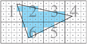
Figure 23.3. A possible traversal order when using tiled traversal with 4×4
The tiles need to be traversed in some order as well, and this can be done in zigzag order or using some space-filling curve [1159], both of which tend to increase coherency. Additional levels in the hierarchical traversal can be added if needed. For example, one can first visit 16×16
The main advantage of tiled traversal over, say, traversing the triangle in scanline order, is that pixels are processed in a more coherent manner, and as a consequence, texels also are visited more coherently. It also has the benefit of exploiting locality better when accessing color and depth buffers. Consider, for example, a large triangle being traversed in scanline order. Texels are cached, so that the most recently accessed texels remain in the cache for reuse. Assume that mipmapping is used for texturing, which increases the level of reuse from the texels in the cache. If we access pixels in scanline order, the texels used at the beginning of the scanline are likely already evicted from the cache when the end of the scanline is reached. Since it is more efficient to reuse texels in the cache, versus fetching them from memory repeatedly, triangles are often traversed in tiles [651,1162]. This gives a great benefit for texturing [651], depth buffering [679], and color buffering [1463]. In fact, textures and depth and color buffers are also stored in tiles much for the same reasons. This will be discussed further in Section 23.4.
Before triangle traversal starts, GPUs typically have a triangle setup stage. The purpose of this stage is to compute factors that are constant over the triangle so that traversal can proceed efficiently. For example, the edge equations’ (Equation 23.2) constants ai
By necessity, clipping is done before triangle setup since clipping may generate more triangles. Clipping a triangle against the view volume in clip space is an expensive process, and so GPUs avoid doing this if not absolutely necessary. Clipping against the near plane is always needed, and this can generate either one or two triangles. For the edges of the screen, most GPUs then use guard-band clipping, a simpler scheme that avoids the more complex full clip process. The algorithm is visualized in Figure 23.4.

Figure 23.4. Guard-bands to attempt to avoid full clipping. Assume that the guard-band region is ±16
23.1.1. Interpolation
In Section 22.8.1, barycentric coordinates were generated as a byproduct of computing the intersection of a ray and a triangle. Any per-vertex attribute, ai
(23.4)
a(u,v)=(1-u-v)a0+ua1+va2,where a(u, v) is the interpolated attribute at (u, v) over the triangle. The definitions of the barycentric coordinates are
(23.5)
u=A1A0+A1+A2,v=A2A0+A1+A2,where Ai

Figure 23.5. Left: a triangle with scalar attributes (a0,a1,a2)
The edge equation in Equation 23.2 can be expressed using the normal of the edge, n2=(a2,b2)
(23.6)
e2(x,y)=e2(p)=n2·((x,y)-p0)=n2·(p-p0),where p=(x,y)
(23.7)
e2(p)=||n2||||p-p0||cosα,where α
(23.8)
(u(x,y),v(x,y))=(A1,A2)A0+A1+A2=(e1(x,y),e2(x,y))e0(x,y)+e1(x,y)+e2(x,y).The triangle setup often computes 1/(A0+A1+A2)

Figure 23.6. Left: in perspective, the projected image of geometry shrinks with distance. Middle: an edge-on triangle projection. Note how the upper half of the triangle covers a smaller portion on the projection plane than the lower half. Right: a quadrilateral with a checkerboard texture. The top image was rendered using barycentric coordinates for texturing, while the bottom image used perspective-correct barycentric coordinates.
Perspective-correct barycentric coordinates require a division per pixel [163,694]. The derivation [26,1317] is omitted here, and instead we summarize the most important results. Since linear interpolation is inexpensive, and we know how to compute (u, v), we would like to use linear interpolation in screen space as much as possible, even for perspective correction. Somewhat surprisingly, it turns out that it is possible to linearly interpolate both a / w and 1 / w over the triangle, where w is the fourth component of a vertex after all transforms. Recovering the interpolated attribute, a, is a matter of using these two interpolated values,
(23.9)
linearlyinterpolated⏞a/w1/w⏟linearlyinterpolated=aww=a.This is the per-pixel division that was mentioned earlier.
A concrete example shows the effect. Say we interpolate along a horizontal triangle edge, with a0=4
Say instead that the w values for the endpoints are w0=1
In practice, we often need to interpolate several attributes using perspective correction over a triangle. Therefore, it is common to compute perspective-correct barycentric coordinates, which we denote (˜u,˜v)
(23.10)
f0(x,y)=e0(x,y)w0,f1(x,y)=e1(x,y)w1,f2(x,y)=e2(x,y)w2.Note that since e0(x,y)=a0x+b0y+c0
(23.11)
(˜u(x,y),˜v(x,y))=(f1(x,y),f2(x,y))f0(x,y)+f1(x,y)+f2(x,y),which need to be computed once per pixel and can then be used to interpolate any attribute with correct perspective foreshortening. Note that these coordinates are not proportional to the areas of the subtriangles as is the case for (u, v). In addition, the denominator is not constant, as is the case for barycentric coordinates, which is the reason why this division must be performed per pixel.
Finally, note that since depth is z / w, we can see in Equation 23.10 that we should not use those equations since they already are divided by w. Hence, zi/wi
23.1.2. Conservative Rasterization
From DirectX 11 and through using extensions in OpenGL, a new type of triangle traversal called conservative rasterization (CR) is available. CR comes in two types called overestimated CR (OCR) and underestimated CR (UCR). Sometimes they are also called outer-conservative rasterization and inner-conservative rasterization. These are illustrated in Figure 23.7.

Figure 23.7. Conservative rasterization of a triangle. All colored pixels belong to the triangle when using outer-conservative rasterization. The yellow and green pixels are inside the triangle using standard rasterization, and only the green pixels are generated using inner-conservative rasterization.
Loosely speaking, all pixels that overlap or are inside a triangle are visited with OCR and only pixels that are fully inside the triangle are visited with UCR. Both OCR and UCR can be implemented using tiled traversal by shrinking the tile size to one pixel [24]. When no support is available in hardware, one can implement OCR using the geometry shader or using triangle expansion [676]. For more information about CR, we refer to the specifications of the respective API. CR can be useful for collision detection in image space, occlusion culling, shadow computations [1930], and antialiasing, among other algorithms.
Finally, we note that all types of rasterization act as a bridge between geometry and pixel processing. To compute the final locations of the triangle vertices and to compute the final color of the pixels, a massive amount of flexible compute power is needed in the GPU. This is explained next.
23.2 Massive Compute and Scheduling
To provide an enormous amount of compute power that can be used for arbitrary computations, most, if not all, GPU architectures employ unified shader architectures using SIMD-processing with multiple threads, sometimes called SIMT-processing or hyperthreading. See Section for a refresher on the terms thread, SIMD-processing, warps, and thread groups. Note that we use the term warp, which is NVIDIA terminology, but on AMD hardware these are instead called waves or wavefronts. In this section, we will first look at a typical unified arithmetic logic unit (ALU) used in GPUs.
An ALU is a piece of hardware optimized for executing a program for one entity, e.g., a vertex or fragment, in this context. Sometimes we use the term SIMD lane instead of ALU. A typical ALU for a GPU is visualized on the left in Figure 23.8.
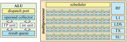
Figure 23.8. Left: an example of an arithmetic logic unit built for execution of one item at a time. The dispatch port receives information about the current instruction to be executed and the operand collector reads the registers required by the instruction. Right: here, 8×4
The main compute units are a floating point (FP) unit and an integer unit. FP units typically adhere to the IEEE 754 FP standard and support a fused-multiply and add (FMA) instruction as one of its most complex instructions. An ALU typically also contains move/compare and load/store capabilities and a branch unit, in addition to transcendental operations, such as cosine, sine, and exponential. It should be noted, however, that some of these may be located in separate hardware units on some architectures, e.g., a small set of, say, transcendental hardware units may operate to serve a larger number of ALUs. This could be the case for operations that are not executed as often as others. These are grouped together in the special unit (SU) block, shown on the right in Figure 23.8. The ALU architecture is usually built using a few hardware pipeline stages, i.e., there are several actual blocks built in silicon that are executed in parallel. For example, while the current instruction performs a multiplication, the next instruction can fetch registers. With n pipeline stages, the throughput can be increased by factor of n, ideally. This is often called pipeline parallelism. Another important reason to pipeline is that the slowest hardware block in a pipelined processor dictates the maximum clock frequency in which the block can be executed. Increasing the number of pipeline stages makes the number of hardware blocks per pipeline stage smaller, which usually makes it possible to increase the clock frequency. However, to simplify the design, an ALU usually has few pipeline stages, e.g., 4–10.
The unified ALU is different from a CPU core in that it does not have many of the bells and whistles, such as branch prediction, register renaming, and deep instruction pipelining. Instead, much of the chip area is spent on duplicating the ALUs to provide massive compute power and on increased register file size, so that warps can be switched in and out. For example, the NVIDIA GTX 1080 Ti has 3584 ALUs. For efficient scheduling of the work that is issued to the GPU, most GPUs group ALUs in numbers of, say, 32. They are executed in lock-step, which means that the entire set of 32 ALUs is a SIMD engine. Different vendors use different names for such a group together with additional hardware units, and we use the general term multiprocessor (MP). For example, NVIDIA uses the term streaming multiprocessor, Intel uses execution unit, and AMD uses compute unit. An example of an MP is shown on the right in Figure 23.8. An MP typically has a scheduler that dispatches work to the SIMD engine(s), and there is also an L1 cache, local data storage (LDS), texture units (TX), and a special unit for handling instructions not executed in the ALUs. An MP dispatches instructions onto the ALUs, where the instructions are executed in lock-step, i.e., SIMD-processing (Section ). Note that the exact content of an MP varies from vendor to vendor and from one architecture generation to the next.
SIMD-processing makes sense for graphics workloads since there are many of the same, e.g., vertices and fragments, that execute the same program. Here, the architecture exploits thread-level parallelism, i.e., the fact that vertices and fragments, say, can execute their shaders independent of other vertices and fragments. Furthermore, with any type of SIMD/SIMT-processing, data-level parallelism is exploited since an instruction is executed for all the lanes in the SIMD machine. There is also instruction-level parallelism, which means that if the processor can find instructions that are independent of each other, they can be executed at the same time, given that there are resources that can execute in parallel.
Close to an MP is a (warp) scheduler that receives large chunks of work that are to be executed on that MP. The task of the warp scheduler is to assign the work in warps to the MP, allocate registers in the register file (RF) to the threads in the warp, and then prioritize the work in the best possible way. Usually, downstream work has higher priority than upstream work. For example, pixel shading is at the end of the programmable stages and has higher priority than vertex shading, which is earlier in the pipeline. This avoids stalling, since stages toward the end are less likely to block earlier stages. See Figure on page 34 for a refresher on the graphics pipeline diagram. An MP can handle hundreds or even thousands of threads in order to hide latency of, for example, memory accesses. The scheduler can switch out the warp currently executing (or waiting) on the MP for a warp that is ready for execution. Since the scheduler is implemented in dedicated hardware, this can often be done with zero overhead [1050]. For instance, if the current warp executes a texture load instruction, which is expected to have long latency, the scheduler can immediately switch out the current warp, replace it with another, and continue execution for that warp instead. In this way, the compute units are better utilized.
Note that for pixel shading work, the warp scheduler dispatches several full quads, since pixels are shaded at quad granularity in order to compute derivatives. This was mentioned in Section 23.1 and will be discussed further in Section 23.8. So, if the size of a warp is 32, then 32/4=8
In general, MPs are also duplicated to obtain higher compute density on the chip, and as a result, a GPU usually has a higher-level scheduler as well. Its task is then to assign work to the different warp schedulers based on work that is submitted to the GPU. Having many threads in a warp generally also means that the work for a thread needs to be independent of the work of other threads. This is, of course, often the case in graphics processing. For example, shading a vertex does not generally depend on other vertices, and the color of a fragment is generally not dependent on other fragments.
Note that there are many differences between architectures. Some of these will be highlighted in Section 23.10, where a few different case studies are presented. At this point, we know how rasterization is done and how shading can be computed using many duplicated unified ALUs. A large remaining piece is the memory system, all the related buffers, and texturing. These are the topics of the following sections starting at Section 23.4, but first we present some more information about latency and occupancy.
23.3 Latency and Occupancy
In general, the latency is the time between making a query and receiving its result. As an example, one may ask for the value at a certain address in memory, and the time it takes from the query to getting the result is the latency. Another example is to request a filtered color from a texture unit, which may take hundreds or possibly even thousands of clock cycles from the time of the request until the value is available. This latency needs to be hidden for efficient usage of the compute resources in a GPU. If these latencies are not hidden, memory accesses can easily dominate execution times.
One hiding mechanism for this is the multithreading part of SIMD-processing, which is illustrated in Figure on page 33. In general, there is a maximum number of warps that an MP can handle. The number of active warps depends on register usage and may also depend on usage of texture samplers, L1 caching, interpolants, and other factors. Here, we define the occupancy, o, as
(23.12)
o=wactivewmax,where wmax
(23.13)
wactive=256·102427·4·32≈75.85,wactive=256·1024150·4·32≈13.65.In the first case, i.e., for the short program using 27 registers, wactive>32
Sometimes a too high occupancy can be counter-productive in that it may thrash the caches if your shaders use many memory accesses [1914]. Another hiding mechanism is to continue executing the same warp after a memory request, which is possible if there are instructions that are independent of the result from the memory access. While this uses more registers, it can sometimes be more efficient to have low occupancy [1914]. An example is loop unrolling, which opens up for more possibilities for instruction-level parallelism, because longer independent instruction chains are often generated, which makes it possible to execute longer before switching warps. However, this would also use more temporary registers. A general rule is to strive after higher occupancy. Low occupancy means that it is less likely to be possible to switch to another warp when a shader requests texture access, for example.
A different type of latency is that from reading back data from the GPU to CPU. A good mental model is to think of the GPU and CPU as separate computers working asynchronously, with communication between the two taking some effort. Latency from changing the direction of the flow of information can seriously hurt performance. When data are read back from the GPU, the pipeline may have to be flushed before the read. During this time, the CPU is waiting for the GPU to finish its work. For architectures, such as Intel’s GEN architecture [844], where the GPU and CPU are on the same chip and use a shared memory model, this type of latency is greatly reduced. The lower-level caches are shared between the CPU and the GPU, while the higher-level caches are not. The reduced latency of the shared caches allows different types of optimization and other kinds of algorithms. For example, this feature has been used to speed up ray tracing, where rays are communicated back and forth between the graphics processor and the CPU cores at no cost [110].
An example of a read-back mechanism that does not produce a CPU stall is the occlusion query. See Section 19.7.1. For occlusion testing, the mechanism is to perform the query and then occasionally check the GPU to see if the results of the query are available. While waiting for the results, other work can then be done on both the CPU and GPU.
23.4 Memory Architecture and Buses
Here, we will introduce some terminology, discuss a few different types of memory architectures, and then present compression and caching.
A port is a channel for sending data between two devices, and a bus is a shared channel for sending data among more than two devices. Bandwidth is the term used to describe throughput of data over the port or bus, and is measured in bytes per second, B/s. Ports and buses are important in computer graphics architecture because, simply put, they glue together different building blocks. Also important is that bandwidth is a scarce resource, and so a careful design and analysis must be done before building a graphics system. Since ports and buses both provide data transfer capabilities, ports are often referred to as buses, a convention we will follow here.
For many GPUs, it is common to have exclusive GPU memory on the graphics accelerator, and this memory is often called video memory. Access to this memory is usually much faster than letting the GPU access system memory over a bus, such as, for example, PCI Express (PCIe), used in PCs. Sixteen-lane PCIe v3 can provide 15.75 GB/s in both directions and PCIe v4 can provide 31.51 GB/s. However, the video memory of the Pascal architecture for graphics (GTX 1080) provides 320 GB/s.
Traditionally, textures and render targets are stored in video memory, but it can serve to store other data as well. Many objects in a scene do not appreciably change shape from frame to frame. Even a human character is typically rendered with a set of unchanging meshes that use GPU-side vertex blending at the joints. For this type of data, animated purely by modeling matrices and vertex shader programs, it is common to use static vertex and index buffers, which are placed in video memory. Doing so makes for fast access by the GPU. For vertices that are updated by the CPU each frame, dynamic vertex and index buffers are used, and these are placed in system memory that can be accessed over a bus, such as PCI Express. One nice property of PCIe is that queries can be pipelined, so that several queries can be requested before results return.
Most game consoles, e.g., all Xboxes and the PLAYSTATION 4, use a unified memory architecture (UMA), which means that the graphics accelerator can use any part of the host memory for textures and different kinds of buffers [889]. Both the CPU and the graphics accelerator use the same memory, and thus also the same bus. This is clearly different from using dedicated video memory. Intel also uses UMA so that memory is shared between the CPU cores and the GEN9 graphics architecture [844], which is illustrated in Figure 23.9.

Figure 23.9. A simplified view of the memory architecture of Intel’s system-on-a-chip (SoC) Gen9 graphics architecture connected with CPU cores and a shared memory model. Note that the last-level caches (LLCs) are shared between both the graphics processor and the CPU cores. (Illustration after Junkins [844].)
However, not all caches are shared. The graphics processor has its own set of L1 caches, L2 caches, and an L3 cache. The last-level cache is the first shared resource in the memory hierarchy. For any computer or graphics architecture, it is important to have a cache hierarchy. Doing so decreases the average access time to memory, if there is some kind of locality in the accesses. In the following section we discuss caching and compression for GPUs.
23.5 Caching and Compression
Caches are located in several different parts of each GPU, but they differ from architecture to architecture, as we will see in Section 23.10. In general, the goal of adding a cache hierarchy to an architecture is to reduce memory latency and bandwidth usage by exploiting locality of memory access patterns. That is, if the GPU accesses one item, it is likely that it will access this same or a nearby item soon thereafter [715]. Most buffers and texture formats are stored in tiled formats, which also helps increase locality [651]. Say that a cache line consists of 512 bits, i.e., 64 bytes, and that the currently used color format uses 4 B per pixel. One design choice would then be to store all the pixels inside a 4×4
To obtain an efficient GPU architecture, one needs to work on all fronts to reduce bandwidth usage. Most GPUs contain hardware units that compress and decompress render targets on the fly, e.g., as images are being rendered. It is important to realize that these types of compression algorithms are lossless; that is, it is always possible to reproduce the original data exactly. Central to these algorithms is what we call the tile table, which has additional information stored for each tile. This can be stored on chip or accessed through a cache via the memory hierarchy. Block diagrams for these two types of systems are shown in Figure 23.10. In general, the same setup can be used for depth, color, and stencil compression, sometimes with some modifications.

Figure 23.10. Block diagrams of hardware techniques for compression and caching of render targets in a GPU. Left: post-cache compression, where the compressor/decompressor hardware units are located after (below) the cache. Right: pre-cache compression, where the compressor/decompressor hardware units are located before (above) the cache.
Each element in the tile table stores the state of a tile of pixels in the framebuffer. The state of each tile can be either compressed, uncompressed, or cleared (discussed next). In general there could also be different types of compressed blocks. For example, one compressed mode might compress down to 25% and another to 50%. It is important to realize that the levels of compression depend on the size of the memory transfers that the GPU can handle. Say the smallest memory transfer is 32 B in a particular architecture. If the tile size is chosen to be 64 B, then it would only be possible to compress to 50%. However, with a tile size of 128 B, one can compress to 75% (96 B), 50% (64 B), and 25% (32 B).
The tile table is often also used to implement fast clearing of the render target. When the system issues a clear of the render target, the state of each tile in the table is set to cleared, and the framebuffer proper is not touched. When the hardware unit accessing the render target needs to read the cleared render target, the decompressor unit first checks the state in the table to see if the tile is cleared. If so, the render target tile is placed in the cache with all values set to the clear value, without any need to read and decompress the actual render target data. In this way, access to the render target itself is minimized during clears, which saves bandwidth. If the state is not cleared, then the render target for that tile has to be read. The tile’s stored data are read and, if compressed, passed through the decompressor before being sent on.
When the hardware unit accessing the render target has finished writing new values, and the tile is eventually evicted from the cache, it is sent to the compressor, where an attempt is made at compressing it. If there are two compression modes, both could be tried, and the one that can compress that tile with fewest bits is used. Since the APIs require lossless render target compression, a fallback to using uncompressed data is needed if all compression techniques fail. This also implies that lossless render target compression never can reduce memory usage in the actual render target—such techniques only reduce memory bandwidth usage. If compression succeeds, the tile’s state is set to compressed and the information is sent in a compressed form. Otherwise, it is sent uncompressed and the state is set to uncompressed.
Note that the compressor and decompressor units can be either after (called post-cache) or before (pre-cache) the cache, as shown in Figure 23.10. Pre-cache compression can increase the effective cache size substantially, but it usually also increases the complexity of the system [681] There are specific algorithms for compressing depth [679,1238,1427] and color [1427,1463,1464,1716]. The latter include research on lossy compression, which, however, is not available in any hardware we know of [1463]. Most of the algorithms encode an anchor value, which represents all the pixels in a tile, and then the differences are encoded in different ways with respect to that anchor value. For depth, it is common to store a set of plane equations [679] or use a difference-of-differences technique [1238], which both give good results since depth is linear in screen space.
23.6 Color Buffering
Rendering using the GPU involves accessing several different buffers, for example, color, depth, and stencil buffers. Note that, though it is called a “color” buffer, any sort of data can be rendered and stored in it.
The color buffer usually has a few color modes, based on the number of bytes representing the color. These modes include:
- High color—2 bytes per pixel, of which 15 or 16 bits are used for the color, giving 32,768 or 65,536 colors, respectively.
- True color or RGB color—3 or 4 bytes per pixel, of which 24 bits are used for the color, giving 16,777,216≈16.8
16,777,216≈16.8 million different colors. - Deep color—30, 36, or 48 bits per pixel, giving at least a billion different colors.
The high color mode has 16 bits of color resolution to use. Typically, this amount is split into at least 5 bits each for red, green, and blue, giving 32 levels per color channel. This leaves one bit, which is usually given to the green channel, resulting in a 5-6-5 division. The green channel is chosen because it has the largest luminance effect on the eye, and so requires greater precision. High color has a speed advantage over true and deep color. This is because 2 bytes of memory per pixel may usually be accessed more quickly than three or more bytes per pixel. That said, the use of high color mode is quite rare to non-existent at this point. Differences in adjacent color levels are easily discernible with only 32 or 64 levels of color in each channel. This problem is sometimes called banding or posterization. The human visual system further magnifies these differences due to a perceptual phenomenon called Mach banding [543,653]. See Figure 23.11. Dithering [102,539,1081], where adjacent levels are intermingled, can lessen the effect by trading spatial resolution for increased effective color resolution. Banding on gradients can be noticeable even on 24-bit monitors. Adding noise to the framebuffer image can be used to mask this problem [1823].
True color uses 24 bits of RGB color, 1 byte per color channel. On PC systems, the ordering is sometimes reversed to BGR. Internally, these colors are often stored using 32 bits per pixel, because most memory systems are optimized for accessing 4-byte elements.

Figure 23.11. As the rectangle is shaded from white to black, banding appears. Although each of the 32 grayscale bars has a solid intensity level, each can appear to be darker on the left and lighter on the right due to the Mach band illusion.
On some systems the extra 8 bits can also be used to store an alpha channel, giving the pixel an RGBA value. The 24-bit color (no alpha) representation is also called the packed pixel format, which can save framebuffer memory in comparison to its 32-bit, unpacked counterpart. Using 24 bits of color is almost always acceptable for real-time rendering. It is still possible to see banding of colors, but much less likely than with only 16 bits.
Deep color uses 30, 36, or 48 bits per color for RGB, i.e., 10, 12, or 16 bits per channel. If alpha is added, these numbers increase to 40/48/64. HDMI 1.3 on supports all 30/36/48 modes, and the DisplayPort standard also has support for up to 16 bits per channel.
Color buffers are often compressed and cached as described in Section 23.5. In addition, blending incoming fragment data with the color buffers is further described in each of the case studies in Section 23.10. Blending is handled by raster operation (ROP) units, and each ROP is usually connected to a memory partition, using, for example, a generalized checkerboard pattern [1160]. We next will discuss the video display controller, which takes a color buffer and makes it appear on the display. Single, double, and triple buffering are then examined.
23.6.1. Video Display Controller
In each GPU, there is a video display controller (VDC), also called a display engine or display interface, which is responsible for making a color buffer appear on the display. This is a hardware unit in the GPU, which may support a variety of interfaces, such as high-definition multimedia interface (HDMI), DisplayPort, digital visual interface (DVI), and video graphics array (VGA). The color buffer to be displayed may be located in the same memory as the CPU uses for its tasks, in dedicated frame-buffer memory, or in video memory, where the latter can contain any GPU data but is not directly accessible to the CPU. Each of the interfaces uses its standard’s protocol to transfer parts of the color buffer, timing information, and sometimes even audio. The VDC may also perform image scaling, noise reduction, composition of several image sources, and other functions.
The rate at which a display, e.g., an LCD, updates the image is typically between 60 and 144 times per second (Hertz). This is also called the vertical refresh rate. Most viewers notice flicker at rates less than 72 Hz. See Section for more information on this topic.
Monitor technology has advanced on several fronts, including refresh rate, bits per component, gamut, and sync. The refresh rate used to be 60 Hz, but 120 Hz is becoming more common, and up to 600 Hz is possible. For high refresh rates, the image is typically shown multiple times, and sometimes black frames are inserted, to minimize smearing artifacts due to the eyes moving during frame display [7,646]. Monitors can also have more than 8 bits per channel, and HDR monitors could be the next big thing in display technology. These can use 10 bits per channel or more. Dolby has HDR display technology that uses a lower-resolution array of LED backlights to enhance their LCD monitors. Doing so gives their display about 10 times the brightness and 100 times the contrast of a typical monitor [1596]. Monitors with wider color gamuts are also becoming more common. These can display a wider range of colors by having pure spectral hues become representable, e.g., more vivid greens. See Section for more information about color gamuts.
To reduce tearing effects, companies have developed adaptive synchronization technologies, such as AMD’s FreeSync and NVIDIA’s G-sync. The idea here is to adapt the update rate of the display to what the GPU can produce instead of using a fixed predetermined rate. For example, if one frame takes 10 ms and the next takes 30 ms to render, the image update to the display will start immediately after each image has finished rendering. Rendering appears much smoother with such technologies. In addition, if the image is not updated, then the color buffer needs not to be sent to the display, which saves power.
23.6.2. Single, Double, and Triple Buffering
In Section 2.4, we mentioned that double buffering ensures that the image is not shown on the display until rendering has finished. Here, we will describe single, double, and even triple buffering.
Assume that we have only a single buffer. This buffer has to be the one that is currently shown on the display. As triangles for a frame are drawn, more and more of them will appear as the monitor refreshes—an unconvincing effect. Even if our frame rate is equal to the monitor’s update rate, single buffering has problems. If we decide to clear the buffer or draw a large triangle, then we will briefly be able to see the actual partial changes to the color buffer as the video display controller transfers those areas of the color buffer that are being drawn. Sometimes called tearing, because the image displayed looks as if it were briefly ripped in two, this is not a desirable feature for real-time graphics. On some ancient systems, such as the Amiga, you could test where the beam was and so avoid drawing there, thus allowing single buffering to work. These days, single buffering is rarely used, with the possible exception of virtual reality systems, where “racing the beam” can be a way to reduce latency [6].

Figure 23.12. For single buffering (top), the front buffer is always shown. For double buffering (middle), first buffer 0 is in front and buffer 1 is in the back. Then they swap from front to back and vice versa for each frame. Triple buffering (bottom) works by having a pending buffer as well. Here, first a buffer is cleared and rendering to it is begun (pending). Second, the system continues to use the buffer for rendering until the image has been completed (back). Finally, the buffer is shown (front).
To avoid the tearing problem, double buffering is commonly used. A finished image is shown in the front buffer, while an offscreen back buffer contains the image that is currently being drawn. The back buffer and the front buffer are then swapped by the graphics driver, typically just after an entire image has been transferred to the display to avoid tearing. Swapping is often done by just swapping two color buffer pointers. For CRT displays, this event is called the vertical retrace, and the video signal during this time is called the vertical synchronization pulse, or vsync for short. For LCD displays, there is no physical retrace of a beam, but we use the same term to indicate that the entire image has just been transferred to the display. Instantly swapping back and front buffers after rendering completes is useful for benchmarking a rendering system, and is also used in many applications because it maximizes frame rate. Not updating on the vsync also leads to tearing, but because there are two fully formed images, the artifact is not as bad as with single buffering. Immediately after the swap, the (new) back buffer is then the recipient of graphics commands, and the new front buffer is shown to the user. This process is shown in Figure 23.12.
Double buffering can be augmented with a second back buffer, which we call the pending buffer. This is called triple buffering [1155]. The pending buffer is like the back buffer in that it is also offscreen, and that it can be modified while the front buffer is being displayed. The pending buffer becomes part of a three-buffer cycle. During one frame, the pending buffer can be accessed. At the next swap, it becomes the back buffer, where the rendering is completed. Then it becomes the front buffer and is shown to the viewer. At the next swap, the buffer again turns into a pending buffer. This course of events is visualized at the bottom of Figure 23.12.
Triple buffering has one major advantage over double buffering. Using it, the system can access the pending buffer while waiting for the vertical retrace. With double buffering, while waiting for the vertical retrace so that a swap can take place, the construction must simply keep waiting. This is so because the front buffer must be shown to the viewer, and the back buffer must remain unchanged because it has a finished image in it, waiting to be shown. The drawback of triple buffering is that the latency increases up to one entire frame. This increase delays the reaction to user inputs, such as keystrokes and mouse or joystick moves. Controls can feel sluggish because these user events are deferred after the rendering begins in the pending buffer.
In theory, more than three buffers could be used. If the amount of time to compute a frame varies considerably, more buffers give more balance and an overall higher display rate, at the cost of more potential latency. To generalize, multibuffering can be thought of as a circular structure. There is a rendering pointer and a display pointer, each pointing at a different buffer. The rendering pointer leads the display pointer, moving to the next buffer when the current rendering buffer is done being computed. The only rule is that the display pointer should never be the same as the rendering pointer.
A related method of achieving additional acceleration for PC graphics accelerators is to use SLI mode. Back in 1998 3dfx used SLI as an acronym for scanline interleave, where two graphics chipsets run in parallel, one handling the odd scanlines and the other the even. NVIDIA (who bought 3dfx’s assets) uses this abbreviation for an entirely different way of connecting two (or more) graphics cards, called scalable link interface. AMD calls it CrossFire X. This form of parallelism divides the work by either splitting the screen into two (or more) horizontal sections, one per card, or by having each card fully render its own frame, alternating output. There is also a mode that allows the cards to accelerate antialiasing of the same frame. The most common use is having each GPU render a separate frame, called alternate frame rendering (AFR). While this scheme sounds as if it should increase latency, it can often have little or no effect. Say a single GPU system renders at 10 FPS. If the GPU is the bottleneck, two GPUs using AFR could render at 20 FPS, or even four at 40 FPS. Each GPU takes the same amount of time to render its frame, so latency does not necessarily change.
Screen resolutions continue to increase, posing a serious challenge to renderers based on per-pixel sampling. One way to maintain frame rate is to adaptively change the pixel shading rate over the screen [687,1805] and surfaces [271].
23.7 Depth Culling, Testing, and Buffering
In this section, we will cover everything that has to do with depth, including resolution, testing, culling, compression, caching, buffering, and early-z.
Depth resolution is important because it helps avoid rendering errors. For example, say you modeled a sheet of paper and placed it on a desk, ever so slightly above the desk’s surface. With precision limits of the z-depths computed for the desk and paper, the desk can poke through the paper at various spots. This problem is sometimes called z-fighting. Note that if the paper were placed exactly at the same height as the desk, i.e., the paper and desk were made coplanar, then there would be no right answer without additional information about their relationship. This problem is due to poor modeling and cannot be resolved by better z precision.
As we saw in Section 2.5.2, the z-buffer (also called the depth buffer) can be used to resolve visibility. This kind of buffer typically has 24 bits or 32 bits per pixel (or sample), and may use floating point or fixed-point representations [1472]. For orthographic viewing, the distance values are proportional to the z-values, and so a uniform distribution is obtained. However, for perspective viewing, the distribution is nonuniform, as we have seen on seen on pages 99-102. After applying the perspective transform (Equations or ), a division by the w-component is required (Equation ). The depth component then becomes pz=qz/qw
The hardware depth pipeline is shown in Figure 23.13.

Figure 23.13. A possible implementation of the depth pipeline, where z-interpolate simply computes the depth value using interpolation. (Illustration after Andersson et al. [46].)
The main goal of this pipeline is to test each incoming depth, generated when rasterizing a primitive, against the depth buffer, and possibly to write the incoming depth to the depth buffer if the fragment passes the depth test. At the same time, this pipeline needs to be efficient. The left part of the figure starts with coarse rasterization, i.e., rasterization on a tile level (Section 23.1). At this point, only tiles that overlap a primitive are passed through to the next stage, called the HiZ unit, where z-culling techniques are executed. The HiZ unit starts with a block called the coarse depth test, and two types of tests are often performed here. We start by describing zmax
- The minimum z-value of the three vertices of a triangle can be used. This is not always accurate, but has little overhead.
- Evaluate the z-value at the four corners of a tile using the plane equation of the triangle, and use the minimum of those.
The best culling performance is obtained if these two strategies are combined. This is done by taking the larger of the two zmin
The other type of coarse depth test is zmin
The green boxes in Figure 23.13 are concerned with different ways to update a tile’s zmax
For tiles that survive the coarse depth test, pixel or sample coverage is determined (using edge equations as described in Section 23.1) and per-sample depths are computed (called z-interpolate in Figure 23.13). These values are forwarded to the depth unit, shown on the right in the figure. Per the API descriptions, pixel shader evaluation should follow. However, under some circumstances, which will be covered below, an additional test, called early-z [1220,1542] or early depth, can be performed without altering the expected behavior. Early-z is actually just the per-sample depth test performed before the pixel shader, and occluded fragments are discarded. This process thus avoids unnecessary execution of the pixel shader. The early-z test is often confused with z-culling, but it is performed by entirely separate hardware. Either technique can be used without the other.
All of zmax
On newer hardware, it may be possible to perform atomic read-modify-write operations, loads, and stores to an image from shaders. In these cases, you can explicitly enable early-z and override these constraints, if you know it is safe to do so. Another feature, which can be used when the pixel shader outputs custom depth, is conservative depth. In this case, early-z can be enabled if the programmer guarantees that the custom depth is greater than the triangle depth. For this example, zmax
As always, occlusion culling benefits from rendering front to back. Another technique with a similar name, and similar intent, is the z-prepass. The idea is that the programmer first renders the scene while writing only depth, disabling pixel shading, and writing to the color buffer. When rendering subsequent passes, an “equal” test is used, meaning that only the frontmost surfaces will be shaded since the z-buffer already has been initialized. See Section 18.4.5.
To conclude this section, we will briefly describe caching and compression for the depth pipeline, which is shown on the lower right of Figure 23.13. The general compression system is similar to the system described in Section 23.5. Each tile can be compressed to a few select sizes, and there is always a fallback to uncompressed data, which is used when compression fails to reach any of the selected sizes. Fast clear is used to save bandwidth usage when clearing the depth buffer. Since depth is linear in screen space, typical compression algorithms either store plane equations with high precision, use a difference-of-differences technique with delta encoding, or use some anchor method [679,1238,1427]. The tile table and the HiZ cache may be stored entirely in on-chip buffers, or they may communicate though the rest of the memory hierarchy, as does the depth cache. Storing on chip is expensive, since these buffers need to be large enough to handle the largest supported resolution.
23.8 Texturing
While texture operations, including fetching, filtering, and decompression, certainly can be implemented in pure software running on the GPU multiprocessors, it has been shown that fixed-function hardware for texturing can be up to 40 times faster [1599]. The texture unit performs addressing, filtering, clamping, and decompression of texture formats (Chapter ). It is used in conjunction with a texture cache to reduce bandwidth usage. We start by discussing filtering and what consequence that has on the texture unit.
To be able to use minification filters, such as mipmapping and anisotropic filtering, the derivatives of the texture coordinates in screen space are needed. That is, to compute the texture level of detail λ
In general, derivative computations happen under the hood, i.e., they are hidden from the user. The actual implementation is often done using cross-lane instructions (shuffle/swizzle) over a quad, and such instructions may be inserted by the compiler. Some GPUs instead use fixed-function hardware to compute these derivatives. There is no exact specification of how derivatives should be computed. Some common methods are shown in Figure 23.14. OpenGL 4.5 and DirectX 11 support functions for both coarse and fine derivatives [1368].

Figure 23.14. Illustration of how derivatives may be computed. Arrows indicate that the difference is computed between the pixel where the arrow ends and the pixel where it starts. For example, the top left horizontal difference is computed as the top right pixel minus the top left pixel. For coarse derivatives (left), a single horizontal difference and a single vertical difference are used for all four pixels within the quad. For fine derivatives (right), one uses the differences closest to the pixel. (Illustration after Penner [1368].)
Texture caching [362,651,794,795] is used by all GPUs to reduce bandwidth usage for textures. Some architectures use a dedicated cache for texturing, or even two dedicated levels of texture caching, while others share a cache between all types of accesses, including texturing. Typically a small on-chip memory (usually SRAM) is used to implement a texture cache. This cache stores the results of recent texture reads, and access is quick. The replacement policies and sizes are architecture-dependent. If neighboring pixels need to access the same or closely located texels, they are likely to find these in the cache. As mentioned in Section 23.4, memory accesses are often done in a tiled fashion, so instead of texels being stored in a scanline order, they are stored in small tiles, e.g., 4×4
(23.14)
A(u,v)=B+(vn-1un-1vn-2un-2⋯v1u1v0u0)·T,where B is the base address of the texture and T is the number of bytes occupied by one texel. The advantage of this remapping is that it gives rise to the texel order shown in Figure 23.15. As can be seen, this is a space-filling curve, called a Morton sequence [1243], and it is known to improve coherency [1825]. In this case, the curve is two-dimensional, since textures normally are, too.

Figure 23.15. Texture swizzling increases coherency of texel memory accesses. Note that texel size here is 4 bytes, and that the texel address is shown in each texel’s upper left corner.
The texture units also contain custom silicon to decompress several different texture formats (Section ). These are usually many times more efficient when implemented in fixed-function hardware, compared to software implementations. Note that when using a texture both as a render target and for texture mapping, other compression opportunities occur. If compression of the color buffer is enabled (Section 23.5), then there are two design options when accessing such a render target as a texture. When the render target has finished its rendering, one option is to decompress the entire render target from its color buffer compression format and to store it uncompressed for subsequent texture accesses. The second option is to add hardware support in the texture unit to decompress the color buffer compression formats [1716]. The latter is the more efficient option, since the render target can stay compressed even during access as a texture. More information about caches and compression can be found in Section 23.4.
Mipmapping is important for texture cache locality, since it enforces a maximum texel-pixel ratio. When traversing a triangle, each new pixel represents a step in texture space of approximately one texel. Mipmapping is one of the few cases in rendering where a technique improves both visuals and performance.
23.9 Architecture
The best way of achieving faster graphics is to exploit parallelism, and this can be done in practically all stages in a GPU. The idea is to compute multiple results simultaneously and then merge these at a later stage. In general, a parallel graphics architecture has the appearance shown in Figure 23.16. The application sends tasks to the GPU, and after some scheduling, geometry processing starts in parallel in several geometry units. The results from geometry processing are forwarded to a set of rasterizer units, which perform rasterization. Pixel shading and blending are then performed, also in parallel, by a set of pixel processing units. Finally, the resulting image is sent to the display for viewing.

Figure 23.16. The general architecture for a high-performance, parallel computer graphics architecture, consisting of several geometry units (G’s), rasterizer units (R’s), and pixel processing units (P’s).
For both software and hardware, it is important to realize that if there is a serial part of your code or hardware, it will limit the amount of total possible performance improvement. This is expressed by Amdahl’s law, i.e.,
(23.15)
a(s,p)=1s+1-sp,where s is the serial percentage of a program/hardware, and hence 1-s
For graphics architectures, multiple results are computed in parallel, but primitives in draw calls are expected to be processed in the order they were submitted by the CPU. Therefore, some kind of sorting must be done, so that the parallel units together render the image that the user intended. Specifically, the sorting needed is from model space to screen space (Section and ). It should be noted that the geometry units and pixel processing units may be mapped to identical units, i.e., unified ALUs. All the architectures in our case study section use unified shader architectures (Section 23.10). Even if this is the case, it is important to understand where this sorting takes place. We present a taxonomy [417,1236] for parallel architectures. The sort can occur anywhere in the pipeline, which gives rise to four different classes of work distribution in parallel architectures, as shown in Figure 23.17. These are called sort-first, sort-middle, sort-last fragment, and sort-last image. Note that these architectures give rise to different ways to distribute work among the parallel units in the GPU.

Figure 23.17. Taxonomy of parallel graphics architectures. A is the application, G’s are geometry units, R’s are rasterizer units, and P’s are pixel processing units. From left to right, the architectures are sort-first, sort-middle, sort-last fragment, and sort-last image. (Illustration after Eldridge et al. [417].)
A sort-first-based architecture sorts primitives before the geometry stage. The strategy is to divide the screen into a set of regions, and the primitives inside a region are sent to a complete pipeline that “owns” that region. See Figure 23.18.

Figure 23.18. Sort-first splits the screen into separate tiles and assigns a processor to each tile, as shown here. A primitive is then sent to the processors whose tiles they overlap. This is in contrast to sort-middle architecture, which needs to sort all triangles after geometry processing has occurred. Only after all triangles have been sorted can per-pixel rasterization start. (Images courtesy of Marcus Roth and Dirk Reiners.)
A primitive is initially processed enough to know which region(s) it needs to be sent—this is the sorting step. Sort-first is the least explored architecture for a single machine [418,1236]. It is a scheme that does see use when driving a system with multiple screens or projectors forming a large display, as a single computer is dedicated to each screen [1513]. A system called Chromium [787] has been developed, which can implement any type of parallel rendering algorithm using a cluster of workstations. For example, sort-first and sort-last can be implemented with high rendering performance.
The Mali architecture (Section 23.10.1) is of the type sort-middle. The geometry processing units are given approximately the same amount of geometry to process. Then transformed geometry is sorted into non-overlapping rectangles, called tiles, that together cover the entire screen. Note that a transformed triangle may overlap with several tiles and so may be processed by several rasterizer and pixel processing units. Key to efficiency here is that each pair of rasterizer and pixel processing units have a tile-sized framebuffer on chip, which means that all framebuffer accesses are fast. When all geometry has been sorted to tiles, rasterization and pixel processing of each tile can commence independently of each other. Some sort-middle architectures perform a z-prepass per tile for opaque geometry, which means that each pixel is only shaded once. However, not all sort-middle architectures do this.
The sort-last fragment architecture sorts the fragments after rasterization (sometimes called fragment generation) and before pixel processing. An example is the GCN architecture, described in Section 23.10.3. Just as with sort-middle, primitives are spread as evenly as possible across the geometry units. One advantage with sort-last fragment is that there will not be any overlap, meaning that a generated fragment is sent to only one pixel processing unit, which is optimal. Imbalance can occur if one rasterizer unit deals with large triangles, while another one deals with only small triangles.

Figure 23.19. In sort-last image, different objects in the scene are sent to different processors. Transparency is difficult to deal with when compositing separate rendered images, so transparent objects are usually sent to all nodes. (Images courtesy of Marcus Roth and Dirk Reiners.)
Finally, the sort-last image architecture sorts after pixel processing. A visualization is shown in Figure 23.19. This architecture can be seen as a set of independent pipelines. The primitives are spread across the pipelines, and each pipeline renders an image with depth. In a final composition stage, all the images are merged with respect to their z-buffers. It should be noted that sort-last image systems cannot fully implement an API such as OpenGL and DirectX, because they require that primitives be rendered in the order they are sent. PixelFlow [455,1235] is an example of the sort-last image architecture. The PixelFlow architecture is also noteworthy because it uses deferred shading, meaning that it shades only visible fragments. It should be noted, however, that no current architectures use sort-last image due to the substantial bandwidth usage toward the end of the pipelines.
One problem with a pure sort-last image scheme for large tiled display systems is the sheer amount of image and depth data that needs to be transferred between rendering nodes. Roth and Reiners [1513] optimize data transfer and composition costs by using the screen and depth bounds of each processor’s results.
Eldridge et al. [417,418] present Pomegranate, a sort-everywhere architecture. Briefly, it inserts sort stages between the geometry stage and the rasterizer units (R’s), between R’s and pixel processing units (P’s), and between P’s and the display. The work is therefore kept more balanced as the system scales (i.e., as more pipelines are added). The sorting stages are implemented as a high-speed network with point-to-point links. Simulations show a nearly linear performance increase as more pipelines are added.
All the components in a graphics system (host, geometry processing, rasterization, and pixel processing) connected together give us a multiprocessing system. For such systems there are two problems that are well known, and almost always associated with multiprocessing: load balancing and communication [297]. FIFO (first-in, first-out) queues are often inserted into many different places in the pipeline, so that jobs can be queued to avoid stalling parts of the pipeline. For example, it is possible to put a FIFO between the geometry and rasterizer units, so that geometry-processed triangles can be buffered if the rasterizer units cannot keep up with the pace of the geometry units, due to huge triangle size, for example.
The different sort architectures described have distinct load balancing advantages and disadvantages. Consult Eldridge’s PhD thesis [418] or the paper by Molnar et al. [1236] for more information on these. The programmer can also affect load balancing; techniques for doing so are discussed in Chapter 18. Communication can be a problem if the bandwidth of the buses is too low, or is used unwisely. Therefore, it is of extreme importance to design an application’s rendering system so that the bottleneck does not occur in any of the buses, e.g., the bus from the host to the graphics hardware. Section deals with different methods to detect bottlenecks.
23.10 Case Studies
In this section, three different graphics hardware architectures will be presented. The ARM Mali G71 Bifrost architecture, targeting mobile devices and televisions, is presented first. NVIDIA’s Pascal architecture follows next. We end with a description of the AMD GCN architecture called Vega.
Note that graphics hardware companies often base their design decisions on extensive software simulations of GPUs that have not yet been built. That is, several applications, e.g., games, are run through their parameterized simulator with several different configurations. Possible parameters are number of MPs, clock frequency, number of caches, number of raster engines/tessellator engines, and number of ROPs, for example. Simulations are used to gather information about such factors as performance, power usage, and memory bandwidth usage. At the end of the day, the best possible configuration, which works best in most use cases, is chosen and a chip is built from that configuration. In addition, simulations may help find typical bottlenecks in the architecture, which then can be addressed, e.g., increasing the size of a cache. For a particular GPU, the reason for various speeds and numbers of units is, simply, “it works best this way.”
23.10.1. Case Study: ARM Mali G71 Bifrost
The Mali product line encompasses all GPU architectures from ARM, and Bifrost is their architecture from 2016. The target for this architecture is mobile and embedded systems, e.g., mobile phones, tablets, and televisions. In 2015, 750 million Mali-based GPUs were shipped. Since many of these are powered by batteries, it is important to design an energy-efficient architecture, rather than just focusing on performance. Therefore, it makes sense to use a sort-middle architecture, where all framebuffer accesses are kept on chip, which lowers power consumption. All Mali architectures are of the sort-middle type, sometimes called a tiling architecture. A high-level overview of the GPU is shown in Figure 23.20.

Figure 23.20. The Bifrost G71 GPU architecture, which is scalable up to 32 shader engines, where each shader engine is the one shown in Figure 23.21. (Illustration after Davies [326].)
As can be seen, the G71 can support up to 32 unified shader engines. ARM uses the term shader core instead of shader engine, but we use the term shader engine to avoid confusion with the rest of the chapter. A shader engine is capable of executing instructions for 12 threads at a time, i.e., it has 12 ALUs. The choice of 32 shader engines was specifically for the G71, but the architecture scales beyond 32 engines.
The driver software feeds the GPU with work. The job manager, i.e., a scheduler, then divides this work among the shader engines. These engines are connected through a GPU fabric, which is a bus on which the engines can communicate with the other units in the GPU. All memory accesses are sent through the memory management unit (MMU), which translates from a virtual memory address to a physical address.
An overview of a shader engine is shown in Figure 23.21.

Figure 23.21. The Bifrost shader engine architecture, where the tile memory is on chip, which makes for fast local framebuffer accesses. (Illustration after Davies [326].)
As can be seen, it contains three execution engines, centered around executing shading for quads. Therefore, they have been designed as a small general-purpose processor with SIMD width 4. Each execution engine contains four fused-multiply-and-add (FMA) units for 32-bit floating point and four 32-bit adders, among other things. This means that there are 3×4
Note that the shader engines are unified and can perform compute, vertex, and pixel shading, to name a few. The execution engine also contains support for many of the transcendental functions, such as sine and cosine. In addition, performance is up to 2×
The core idea of tiling architectures (sort-middle) is to first perform all geometry processing, so that the screen-space position of each primitive to render is found. At the same time, a polygon list, containing pointers to all the primitives overlapping a tile, is built for each tile in the framebuffer. After this step, the set of primitives overlapping a tile is known. Hence, the primitives in a tile can be rasterized and shaded, and the results are stored in the on-chip tile memory. When the tile has finished rendering all its primitives, the data from the tile memory is written back to external memory through the L2 cache. This reduces memory bandwidth usage. Then the next tile is rasterized, and so on, until the entire frame has been rendered. The first tiling architecture was Pixel-Planes 5 [502], and that system has some high-level similarities to the Mali architectures.
Geometry processing and pixel processing are visualized in Figure 23.22.

Figure 23.22. Illustration of how the geometry flows through the Bifrost architecture. The vertex shader consists of position shading, which is used by the tiler, and varying shading which is executed only when needed, after tiling. (Illustration after Choi [264].)
As can be seen, the vertex shader is split into one part that only performs position shading and another part called varying shading, which is done after tiling. This saves memory bandwidth compared to ARM’s previous architectures. The only information needed to perform binning, i.e, determining which tiles a primitive overlaps, is the position of the vertices. The tiler unit, which performs binning, works in a hierarchical fashion as illustrated in Figure 23.23.

Figure 23.23. The hierarchical tiler of the Bifrost architecture. In this example, binning is done on three different levels, where each triangle has been assigned to the level at which it overlaps a single square. (Illustration after Bratt [191].)
This helps make the memory footprint for binning smaller and more predictable, since it is no longer proportional to primitive size.
When the tiler has finished binning all primitives in the scene, it is known exactly which primitives overlap a certain tile. As such, the remaining rasterization, pixel processing, and blending can be performed in parallel for any number of tiles, as long as there are available shader engines that can work in parallel. In general, a tile is submitted to a shader engine that handles all the primitives in that tile. While this work is done for all the tiles, it is also possible to start with geometry processing and tiling for the next frame. This processing model implies that there may be more latency in a tiling architecture.
At this point, rasterization, pixel shader execution, blending, and other per-pixel operations follow. The single most important feature of a tiling architecture is that the framebuffer (including color, depth, and stencil, for example) for a single tile can be stored in quick on-chip memory, here called the tile memory. This is affordable because the tiles are small ( 16×16
Bifrost supports pixel local storage (PLS), which is a set of extensions that generally are supported on sort-middle architectures. Using PLS, one can let the pixel shader access the color of the framebuffer and hence implement custom blending techniques. In contrast, blending is usually configured using the API and is not programmable in the way that a pixel shader is. One can also store arbitrary fixed-size data structures per pixel using the tile memory. This allows the programmer to implement, for example, deferred shading techniques efficiently. The G-buffer (e.g., normal, position, and diffuse texture) is stored in PLS in a first pass. The second pass performs the lighting calculations and accumulates the results in PLS. The third pass uses the information in the PLS to compute the final pixel color. Note that, for a single tile, all these computations occur while the entire tile memory is kept on the chip, which makes it fast.
All Mali architectures have been designed from the ground up with multisampling antialiasing (MSAA) in mind, and they implement the rotated grid supersampling (RGSS) scheme described on page 143, using four samples per pixel. Sort-middle architectures are well suited for antialiasing. This is because filtering is done just before the tile leaves the GPU and is sent out to external memory. Hence, the framebuffer in external memory needs to store only a single color per pixel. A standard architecture would need a framebuffer to be four times as large. For a tiling architecture, you need to increase only the on-chip tile buffer by four times, or effectively use smaller tiles (half the width and height).
The Mali Bifrost architecture can also selectively choose to use either multisampling or supersampling on a batch of rendering primitives. This means that the more expensive supersampling approach, where you execute the pixel shader for each sample, can be used when it is needed. An example would be rendering a textured tree with alpha mapping, where you need high-quality sampling to avoid visual artifacts. For these primitives, supersampling could be enabled. When this complex situation ends and simpler objects are to be rendered, one can switch back to using the less expensive multisampling approach. The architecture also supports 8×
Bifrost (and the previous architecture called Midgard) also supports a technique called transaction elimination. The idea is to avoid memory transfers from the tile memory to off-chip memory for parts of a scene that do not change from frame to frame. For the current frame, a unique signature is computed for each tile when the tile is evicted to the off-chip framebuffer. This signature is a type of checksum. For the next frame, the signature is computed for tiles that are about to be evicted. If the signature from the previous frame is the same as the signature for the current frame for a certain tile, then the architecture avoids writing out the color buffer to off-chip memory since the correct content is already there. This is particularly useful for casual mobile games (e.g., Angry Birds), where a smaller percentage of the scene is updated each frame. Note also that this type of technique is difficult to implement on sort-last architectures, since they do not operate on a per-tile basis. The G71 also supports smart composition, which is transaction elimination applied to user interface composition. It can avoid reading, compositing, and writing a block of pixels if all sources are the same as the previous frame’s and the operations are the same.
Low-level power-saving techniques, such as clock gating and power gating, are also heavily used in this architecture. This means that unused or inactive parts of the pipeline are shut down or kept idle at lower energy consumption to reduce power usage. To reduce texture bandwidth, there is a texture cache with dedicated decompression units for ASTC and ETC. In addition, compressed textures are stored in compressed form in the cache, as opposed to decompressing them and then putting the texels in the cache. This means that when a request for a texel is made, the hardware reads the block from the cache and then decompresses the texels of the block on the fly. This configuration increases the effective size of the cache, which boosts efficiency.
An advantage of the tiling architecture, in general, is that it is inherently designed parallel processing of tiles. For example, more shader engines could be added, where each shader engine is responsible for independently rendering to a single tile at a time. A disadvantage of tiling architectures is that the entire scene data needs to be sent to the GPU for tiling and processed geometry streamed out to memory. In general, sort-middle architectures are not ideal for handling geometry amplification such as applying geometry shaders and tessellation, since more geometry adds to the amount of memory transfers for shuffling geometry back and forth. For the Mali architecture, both geometry shading (Section ) and tessellation are handled in software on the GPU, and the Mali best practices guide [69] recommends never using the geometry shader. For most content, sort-middle architectures work well for mobile and embedded systems.
23.10.2. Case Study: NVIDIA Pascal
Pascal is a GPU architecture built by NVIDIA. It exists both as a graphics part [1297] and as a compute part [1298], where the latter targets high-performance computing and deep learning applications. In this presentation, we will focus mostly on the graphics part, and in particular on a certain configuration called the GeForce GTX 1080. We will present the architecture in a bottom-up fashion, starting with the smallest unified ALU and then building up toward the entire GPU. We will mention some of the other chip configurations briefly at the end of this section.
The unified ALU—CUDA core in NVIDIA terminology—used in the Pascal graphics architecture has the same high-level diagram as the ALU on the left in Figure 23.8 on page 1002. The focus of the ALUs is on floating point and integer arithmetic, but they also support other operations. To increase computational power, several such ALUs are combined into a streaming multiprocessor (SM). In the graphics part of Pascal, the SM consists of four processing blocks, where each block has 32 ALUs. This means that the SM can execute 4 warps of 32 threads at the same time. This is illustrated in Figure 23.24.

Figure 23.24. The Pascal streaming multiprocessor (SM) has 32×2×2
Each processing block, i.e., a SIMT engine with width 32, also has 8 load/store (LD/ST) units and 8 special function units (SFUs). The load/store units handle reading and writing values to registers in the register file, which is 16,384×4
All ALUs in the SM share a single instruction cache, while each SIMT engine has its own instruction buffer with a local set of recently loaded instructions to further increase the instruction cache hit ratio. The warp scheduler is capable of dispatching two warp instructions per clock cycle [1298], e.g., work can be scheduled to both the ALUs and the LD/ST units in the same clock cycle. Note that there are also two L1 caches per SM, each having 24 kB of storage, i.e., 48 kB per SM. The reason to have two L1 caches is likely that a larger L1 cache would need more read and write ports, which increases the complexity of the cache and makes the implementation larger on chip. In addition, there are 8 texture units per SM.
Because shading must be done in 2×2
The SM works in conjunction with the polymorph engine (PM). This unit was introduced in its first incarnation in the Fermi chip [1296]. The PM performs several geometry-related tasks, including vertex fetch, tessellation, simultaneous multi-projection, attribute setup, and stream output. The first stage fetches vertices from a global vertex buffer and dispatches warps to SMs for vertex and hull shading. Then follows an optional tessellation stage (Section ), where newly generated (u, v) patch coordinates are dispatched to the SMs for domain shading and, optionally, geometry shading. The third stage handles viewport transform and perspective correction. In addition, an optional simultaneous multi-projection step is executed here, which can be used for efficient VR rendering, for example (Section ). Next comes an optional fourth stage, where vertices are streamed out to memory. Finally, the results are forwarded to the relevant raster engines.
A raster engine has three tasks, namely, triangle setup, triangle traversal, and z-culling. Triangle setup fetches vertices, computes edge equations, and performs backface culling. Triangle traversal uses a hierarchical tiled traversal technique to visit the tiles overlapping a triangle. It uses the edge equations to perform tile tests and to perform the inside tests. On Fermi, each rasterizer can process up to 8 pixels per clock cycle [1296]. There are no public numbers for this on Pascal. The z-culling unit handles culling on a per-tile basis using the techniques described in Section 23.7. If a tile is culled, then processing is immediately terminated for that tile. For surviving triangles, per-vertex attributes are converted into plane equations for efficient evaluation in the pixel shader.
A streaming processor coupled with a polymorph engine is called a texture processing cluster (TPC). On a higher level, five TPCs are grouped into a graphics processing cluster (GPC) that has a single raster engine serving these five TPCs. A GPC can be thought of as a small GPU, and its goal is to provide a balanced set of hardware units for graphics, e.g., vertex, geometry, raster, texture, pixel, and ROP units. As we will see at the end of this section, creating separate functional units allows designers to more easily create a family of GPU chips with a range of capabilities.
At this point, we have most of the building blocks for the GeForce GTX 1080. It consists of four GPCs, and this general setup is shown in Figure 23.25.

Figure 23.25. The Pascal GPU in its GTX 1080 configuration with 20 SMs, 20 polymorph engines, 4 raster engines, 8×20=160
Notice that there is another level of scheduling here, powered by the GigaThread engine, along with an interface to PCIe v3. The GigaThread engine is a global work distribution engine that schedules blocks of threads to all the GPCs.
The raster operation units are also displayed in Figure 23.25, albeit somewhat hidden. They are located immediately above and below the L2 cache in the middle of the figure. Each blue block is one ROP unit, and there are 8 groups, each with 8 ROPs for a total of 64. The major tasks of the ROP units are to write output to pixels and other buffers, and to perform various operations such as blending. As can be seen on the left and right in the figure, there are a total of eight 32-bit memory controllers, which sums to 256 bits in total. Eight ROP units are tied to a single memory controller and 256 kB of the L2 cache. This gives a total of 2 MB of the L2 cache for the entire chip. Each ROP is tied to a certain memory partition, which means that a ROP handles a certain subset of the pixels in a buffer.
The ROP units also handle lossless compression. There are three different compression modes in addition to supporting uncompressed and fast clears [1297]. For 2 : 1 compression (e.g., from 256 B to 128 B), a reference color value is stored per tile and the differences are encoded between pixels, where each difference is encoded with fewer bits than its uncompressed form. Then 4 : 1 compression is an extension of the 2 : 1 mode, but this mode can only be enabled if the differences can be encoded using even fewer bits, and it works for only those tiles with smoothly varying content. There is also an 8 : 1 mode, which is a combination of 4 : 1 constant color compression of 2×2
The video memory used is GDDRX5 with a clock rate of 10 GHz. Above we saw that the eight memory controllers provide 256 bits = 32 B in total. This gives a total of 320 GB/s of total peak memory bandwidth, but the many levels of caching combined with the compression techniques give an impression of a higher effective rate.

Figure 23.26. The rendered image is shown on the left, while the compression results are visualized for Maxwell (middle), the architecture before Pascal, and for Pascal (right). The more purple the image is, the higher the success rate of buffer compression. (Images from NVIDIA white paper [1297].)
The base clock frequency of the chip is 1607 MHz, and it can operate in boost mode (1733 MHz) for when there is sufficient power budget. The peak compute capability is
(23.16)
2⏟FMA·2560⏟num.SPs·1733⏟clockfreq.=8,872,960MFLOPS≈8.9TFLOPS,where the 2 comes from the fact that a fused-multiply-and-add often is counted as two floating point operations and we have divided by 106
NVIDIA has developed sort-last fragment architectures for a long time. However, since Maxwell, they also support a new type of rendering called tiled caching, which is somewhat between sort-middle and sort-last fragment. This architecture is illustrated in Figure 23.27.

Figure 23.27. Tiled caching introduces a binner that sorts geometry into tiles and lets the transformed geometry stay in the L2 cache. The currently processed tile also stays in L2 until the geometry in that tile for the current chunk is done.
The idea is to exploit locality and the L2 cache. Geometry is processed in small enough chunks so that the output can stay in this cache. In addition, the framebuffer stays in L2 as well, as long as the geometry overlapping that tile has not finished pixel shading.
There are four raster engines in Figure 23.25, but as we know the graphics APIs must (in most cases) respect primitive submission order [1598]. The framebuffer is often split into tiles using a generalized checkerboard pattern [1160], and each raster engine “owns” a set of the tiles. The current triangle is sent to each raster engine that has at least one of its tiles overlapping with the triangle, which solves the ordering problem independently for each tile. This makes for better load balancing. There are usually also several FIFO queues in a GPU architecture, which are there to reduce starvation of hardware units. These queues are not shown in our diagrams.
The display controller has 12 bits per color component and has BT.2020 wide color gamut support. It also supports HDMI 2.0b and HDCP 2.2. For video processing, it supports SMPTE 2084, which is a transfer function for high dynamic range video.
Venkataraman [1816] describes how NVIDIA architectures from Fermi and after have one or more copy engines. These are memory controllers that can perform direct memory access (DMA) transfers. A DMA transfer occur between the CPU and the GPU, and such a transfer is typically started on either of these. The starting processing unit can continue doing other computations during the transfer. The copy engines can initiate DMA transfers of data between the CPU and the GPU memory, and they can execute independently of the rest of the GPU. Hence, the GPU can render triangles and perform other functions while information is transferred from the CPU to the GPU or vice versa.
The Pascal architecture can also be configured for non-graphical applications, such as for training neural networks or large-scale data analysis. The Tesla P100 is one such configuration [1298]. Some of the differences from the GTX 1080 include that it uses high-bandwidth memory 2 (HBM2) with 4096 bits for the memory bus, providing a total memory bandwidth of 720 GB/s. In addition, they have native 16-bit floating point support, with up to 2×
The GTX 1080 Ti (titanium) is a higher-end configuration. It has 3584 ALUs, a 352-bit memory bus, 484 GB/s in total memory bandwidth, 88 ROPs, and 224 texture units, compared to 2560, 256-bit, 320 GB/s, 64, and 160 for the GTX 1080. It is configured using six GPCs, i.e., it has six raster engines, compared to four in the GTX 1080. Four of the GPCs are exactly the same as in the GTX 1080, while the remaining two are somewhat smaller with only four TPCs instead of five. The 1080 Ti is built from 12 billion transistors for the chip, while the 1080 uses 7.2 billion. The Pascal architecture is flexible in that it can also scale down. For example, the GTX 1070 is a GTX 1080 minus one GPC, and the GTX 1050 consists of two GPCs, each with three SMs.
23.10.3. Case Study: AMD GCN Vega
The AMD Graphics Core Next (GCN) architecture is used in several AMD graphics card products as well as in the Xbox One and PLAYSTATION 4. Here, we describe general elements of the GCN Vega architecture [35], which is an evolution of the architectures used in these consoles.
A core building block of the GCN architecture is the compute unit (CU), which is illustrated in Figure 23.28.

Figure 23.28. The GCN compute unit of the Vega architecture. Each of the vector register files has a 64 kB capacity, while the scalar RF has 12.5 kB, and local data share has 64 kB. Note that there are four units of 16 SIMD lanes (light green), with 32-bit floating point, for compute in each CU. (Illustration after Mah [1103] and AMD white paper [35].)
The CU has four SIMD units, each having 16 SIMD lanes, i.e., 16 unified ALUs (using the terminology from Section 23.2). Each SIMD unit executes instructions for 64 threads, which is called a wavefront. One single-precision floating point instruction per clock cycle can be issued per SIMD unit. Because the architecture processes a wavefront of 64 threads per SIMD unit, it takes 4 clock cycles before a wavefront has been fully issued [1103]. Note also that a CU can run code from different kernels at the same time. Since each SIMD unit has 16 lanes and one instruction can be issued per clock cycle, the maximum throughput for the entire CU is 4 SIMD units per CU ×
Each CU has an instruction cache (not shown in the figure) that is shared between up to four SIMD units. The relevant instructions are forwarded to a SIMD unit’s instruction buffer (IB). Each IB has storage for handling 10 wavefronts, which can be switched in and out of the SIMD unit as needed in order to hide latency. This means that the CU can handle 40 wavefronts. This, in turn, is equivalent to 40·64=2560
The scalar unit is a 64-bit ALU that is shared between the SIMD units as well. It has its own scalar register file and a scalar data cache (not shown). The scalar RF has 800 32-bit registers per SIMD unit, i.e., 800·4·4=12.5

Figure 23.29. A Vega 10 GPU built with 64 CUs. Note that each CU contains the hardware shown in Figure 23.28. (Illustration after AMD white paper [35].)
The Vega 10 architecture [35] is illustrated in Figure 23.29. The top part includes a graphics command processor, two hardware schedulers (HWSs) and eight asynchronous compute engines (ACEs) [33]. The task of the GPC is to dispatch graphics tasks onto the graphics pipelines and compute engines of the GPU. The HWSs’ buffers work in queues that they assign to the ACEs as soon as it is possible. The task of an ACE is to schedule compute tasks onto the compute engines. There are also two DMA engines that can handle copy tasks (not shown in the figure). The GPC, ACEs, and DMA engines can work in parallel and submit work to the GPU, which improves utilization, since tasks can be interleaved from different queues. Work can be dispatched from any queue without waiting for other work to finish, which means that independent tasks can execute on the compute engines simultaneously. The ACEs can synchronize via cache or memory. They can support task graphs together, so that one ACE’s task can depend on another ACE’s task, or on the graphics pipeline’s tasks. It is recommended that smaller compute and copy tasks are interleaved with heavier graphics tasks [33].
As can be seen in Figure 23.29, there are four graphics pipelines and four compute engines. Each compute engine has 16 CUs, which sums to 64 CUs in total. The graphics pipeline has two blocks, namely a geometry engine and draw-stream binning rasterizer (DSBR). The geometry engine includes a geometry assembler, tessellation unit, and vertex assembler. In addition, a new primitive shader is supported. The idea of the primitive shader is to enable more flexible geometry processing and faster culling of primitives [35]. The DSBR combines the advantages of sort-middle and sort-last architectures, which also is the goal of tiled caching (Section 23.10.2). The image is divided into tiles in screen space, and after geometry processing, each primitive is assigned to the tiles they overlap. During rasterization of a tile, all data (e.g., tile buffers) required are kept in the L2 cache, which improves performance. Pixel shading can be deferred automatically until all the geometry in a tile has been processed. Hence, a z-prepass is done under the hood and pixels shaded only once. Deferred shading can be turned on and off; e.g., for transparent geometry it needs to be off.
To handle depth, stencil, and color buffers, the GCN architecture has a building block called the color and depth block (CDB). They handle color, depth, and stencil read and writes, in addition to color blending. A CDB can compress the color buffer using the general approach described in Section 23.5. A delta compression technique is used where one pixel’s color is stored uncompressed per tile, and the rest of the color values are encoded relative to that pixel color [34,1238]. In order to increase efficiency, the tile size can be dynamically chosen based on access patterns. For a tile originally stored using 256 bytes, the maximum rate is 8 : 1, i.e., compression down to 32 bytes. A compressed color buffer can be used as a texture in a subsequent pass, in which case the texture unit will decompress the compressed tile, which provides further bandwidth savings [1716].
The rasterizers can rasterize up to four primitives per clock cycle. The CDBs connected to the graphics pipeline and compute engine can write 16 pixels per clock cycle. That is, triangles smaller than 16 pixels reduce efficiency. The rasterizer also handles coarse depth testing (HiZ) and hierarchical stencil testing. The buffer for HiZ is called HTILE and can be programmed by the developer, e.g., for feeding occlusion information to the GPU.
The cache hierarchy of Vega is shown in Figure 23.30. At the top of the hierarchy (rightmost in the figure), we have registers, followed by the L1 and L2 caches. Then, there is high-bandwidth memory 2 (HBM2), which is located on the graphics card as well, and finally system memory located on the CPU side. A new feature of Vega is the High-Bandwidth Cache Controller (HBCC), shown at the bottom of Figure 23.29. It allows the video memory to behave like a last-level cache. This means that if a memory access is made and the corresponding content is not in the video memory, i.e., HBM2, then the HBCC will automatically fetch the relevant system memory page(s) over the PCIe bus and put it in video memory. Less recently used pages in the video memory may be swapped out as a consequence. The memory pool shared between the HBM2 and system memory is called the HBCC memory segment (HMS). All graphics blocks also access memory through the L2 cache, which differs from previous architectures.

Figure 23.30. The cache hierarchy of the Vega architecture.
The architecture also supports virtual memory (Section ).
Note that all the on-chip blocks, e.g., HBCC, XDMA (CrossFire DMA), PCI express, display engines, and multimedia engines, communicate over an interconnect called the Infinity Fabric (IF). AMD CPUs can also be connected to the IF. The Infinity Fabric can connect blocks on different chip dies. The IF is also coherent, meaning that all blocks get to see the same view of the content in memory.
The base clock frequency of the chip is 1677 MHz, i.e., the peak compute capability is
(23.17)
2⏟FMA·4096⏟numSPs·1677⏟clockfreq.=13,737,984MFLOPS≈13.7TFLOPS,where the FMA and TFLOPS calculations match those in Equation 23.16. The architecture is flexible and extendable, so many more configurations are expected.
23.11 Ray Tracing Architectures
This section will give a brief introduction to ray tracing hardware. We will not list all recent references on this topic, but rather provide a set of pointers that the reader is encouraged to follow. Research in this field was started by Schmittler et al. [1571] in 2002, where focus was on traversal and intersection, and shading was computed using a fixed-function unit. This work was later followed up by Woop et al. [1905], who presented an architecture with programmable shaders.
The commercial interest in this topic has increased considerably over the past few years. This can be seen in the fact that companies, such as Imagination Technologies [1158], LG Electronics [1256], and Samsung [1013], have presented their own hardware architectures for real-time ray tracing. However, only Imagination Technologies has released a commercial product at the time of writing.
There are several common traits in these architectures. First, they often use a bounding volume hierarchy based on axis-aligned bounding boxes. Second, they tend to reduce hardware complexity by reducing precision in the ray/box intersection tests (Section ). Finally, they use programmable cores to support programmable shading, which is more or less a requirement today. For example, Imagination Technologies extend their traditional chip design by adding a ray tracing unit, which can exploit the shader cores for shading, for example. The ray tracing unit consists of a ray intersection processor and a coherency engine [1158], where the latter gathers rays with similar properties and processes them together to exploit locality for faster ray tracing. The architecture from Imagination Technologies also includes a dedicated unit for building BVHs.
Research in this field continues to explore several areas, including reduced precision for efficient implementation of traversal [1807], compressed representations for BVHs [1045], and energy efficiency [929]. There is undoubtedly more research to be done.
Further Reading and Resources
A great set of resources are the course notes on computer graphics architectures by Akeley and Hanrahan [20] and Hwu and Kirk [793]. The book by Kirk and Hwu [903] is also an excellent resource for information about programming with CUDA on GPUs. The annual High-Performance Graphics and SIGGRAPH conference proceedings are good sources for presentations on new architectural features. Giesen’s trip down the graphics pipeline is a wonderful online resource for anyone wanting to learn more about the details of GPUs [530]. We also refer the interested reader to Hennessy and Patterson’s book [715] for detailed information about memory systems. Information on mobile rendering is scattered among many sources. Of note, the book GPU Pro 5 has seven articles on mobile rendering techniques.