
1
Optical Switches
Rajan Agrahari1, Sambit Kumar Ghosh2, and Somak Bhattacharyya2
1 Department of Electronics and Communication Engineering, National Institute of Technology, Patna, Bihar, India
2 Department of Electronics Engineering, Indian Institute of Technology (BHU), Varanasi, Uttar Pradesh, India
1.1 Introduction
Any communication system needs three essential components, viz., a source, a receiver, and a medium of transmission. The terminology changes depending on the mode of the communication systems. In modern‐day optical communication, a semiconductor laser has been generally used as the source and optical fiber as the transmission medium. The demand for bandwidth is increasing with the introduction of new applications, viz., grid computing, smart TV systems with live internet broadcasting services, etc. The emergence of three‐dimensional (3D) movies in multiplexes, as well as in‐home entertainment systems, demands more bandwidth of data transmission through optical communication. In order to enhance the transmission rate and bandwidth available on the optical fiber, the other ends of the optical network system need to be improved. The other ends of the optical network include a range of detectors, multiplexers, switches, and buffers [1, 2].
A switch is embedded in the optical communication system to route the message signal under the supervision of the control signals. The message signal could be large in size or a large block of multiplexed data traffic or a series of lower bit channels to be delivered to the users of an optical communication system. An optical switch is versatile in nature as it has a large number of usages in communication networks as well as in communication cores of modern‐day high configuration computers with data rates of 1000 Gbps. With the advent of time, quantum computers have been developed for secure and ultrahigh‐speed communications [3]. New computer architecture needs newly designed optical switches with the least interruption in the phase information of the quantum data packets. The main function of an optical switch is to selectively switch an optical signal transmitting through an optical fiber or one highly configured integrated optical circuit to another [4, 5]. A number of switching mechanisms are associated with optical communication systems. They are summarized in a brief way in different sections of this chapter.
1.2 Electro‐Optical Switching
Fiber‐optic communication systems are experiencing a gradually increasing demand for digital smart TV, digital video and broadband internet services, and many other applications. These types of communication networks should be compatible enough to accommodate future demands of applications at the cost of robust, reliable, and cheap components for information transmission and switching. Optical switches are an integral part of optical networks and fiber‐optic communication systems. Several compound semiconductors, viz., gallium arsenide (GaAs) or indium phosphide (InP) with the integration of photodetectors and lasers have been excessively used as optical switches due to their flexible nature. But the practical realization of these types of devices is costly. Different types of integration technologies have been introduced thereafter with some of the demerits too, viz., silica or/and glass on silicon configurations are used in integrated optical systems but monolithic integration with photodetectors and lasers is not possible. Optical switches made of polymer have also been used but their stability is not good at all [6]. This section will focus on the progress of the electro‐optical switching technology as it is using an improved fabrication process. Recently, liquid crystals of graphene oxide have also been used as an electro‐optical switch [7].
1.2.1 Working Principle of Electro‐Optical Switches
Electro‐optical switching works on various principles, as described below.
(a) Single‐Mode Principle: A ridge waveguide is primarily taken for the formation of the optical switches. The design of a single‐mode ridge waveguide has to fulfill certain design considerations. First, a ridge waveguide should have a numerical aperture equivalent in size to that of a single‐mode fiber. Second, it must contain a large cross‐sectional area equivalent to the core diameter of a single‐mode fiber. Lastly, the waveguide supports the single‐mode operation. A small pictorial description of a silicon‐germanium‐based ridge waveguide is shown in Figure 1.1.
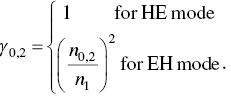
The structure is formed using a Si‐Ge layer of the refractive index of n1 deposited on a Si substrate with refractive index n2. The width (W) of the ridge is 2aλ following a height (h) = 2bλ. The etching depth of the ridge is determined by the term, h′ = 2b(1 − r)λ, where λ is a free‐space optical wavelength, and r is the fractional height of the tapered portions of the rige waveguide. Here, n0, n1, and n2 are the refractive index of free space, Si‐Ge layer, and Si substrate, respectively. All these refractive indices are considered at the operational wavelength. The ratio of the lateral to transverse lengths must obey the condition stated in equation (1.1) and (1.2) [6] for the proper propagation of light within the input and output waveguides.
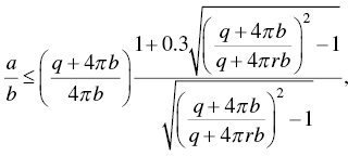
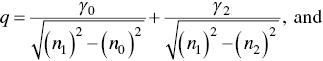

Figure 1.1 Schematic of a Si‐Ge/Si ridge waveguide.
(b) Multimode Principle: The evolution of the multimode interference principle has come into the picture owing to its benefits in terms of easy fabrication, compact size, low loss, and fabrication tolerances. The multimode interference (MMI) switch works on the self‐imaging principle. In this process, an input field is regenerated in terms of one or many images at periodic instances during the propagation of the light. The effective width of a multimode waveguide is represented in equation (1.4) [6], where WM stands for the width of the multimode waveguide, nc is the effective refractive index of the cladding region, and nr is denoted as the effective refractive index of the waveguide. The values of σ are zero and one for TE mode and TM mode, respectively [6].

(c) Plasma Dispersion Effect: In this method, the carrier concentration of the materials determines the refractive index. Equation (1.5) can validate this fact clearly [6].
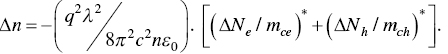
Here q is a charge of an electron, n is the refractive index of the less concentrated SiGe/Si material, c stands for the speed of light in free space, ε0 is free‐space permittivity, ∆Nh and ∆Ne are the change in concentrations of holes and electrons and mch and mce are conductivity effective masses of the holes and electrons of the SiGe/Si material. For example, taking SiGe/Si material when the concentration of Ge is less than 20%, the plasma dispersion effect comes into play to alter the values of refractive indices [6].
1.2.2 Realization of Electro‐Optical Switches
Electro‐optical waveguide switches have been developed using Si‐based components, polymers and lithium niobate (LiNbO3), etc. Silicon‐germanium (SiGe) has been used in the production of multifunctional photonics‐based switching technology because of its less propagation loss within the wavelength region 1.3–1.55 μm. Epitaxial growth of SiGe material is in demand as this process of device realization is compatible with large‐scale silicon integration. Germanium (Ge) is preferable in the electro‐optical switching technology as it has a shorter bandgap and the higher mobility of the electrons. Silicon‐based electro‐optical switches were usually developed using chemical vapor deposition (CVD) techniques and molecular beam epitaxial (MBE) growth. The details of these fabrication processes can be found elsewhere [8].
1.3 Acoustic‐Optical Switching
Acoustic‐optical switching deals with the acoustic‐optic effect, where mainly the refractive index of the medium involved with the optical communication system is altered by the acoustic waves [9, 10]. The periodical strain is generated within the optical communication medium in terms of simultaneous compressions and rarefactions. The acoustic waves are generated with the help of the piezoelectric materials either in the bulk of the material or on the surface of the said material. An RF signal has been used as the driver excitation for producing the acoustic‐optic effect. The electrodes between which the RF electric field has been applied are called the acoustic transducers.
1.3.1 Types of Acoustic‐Optical Switching
Several types of acoustic‐optical switching have been evolved through the years, such as modulators, tunable filters, switches, deflectors, frequency shifters, etc. [11].
(a) Acoustic‐Optical Modulator: An acoustic‐optical modulator is used for the ultimate control of the power of a laser beam while the input excitation signal is an electrical signal. In this case, the refractive index of the optical medium, such as glass or some other crystal is altered by the mechanical strain generated by the oscillation of a sound wave, also called a photo‐elastic effect.

where ∆ηij is the change in refractive index due to mechanical strain, Skl is the strain (a tensor generating from the propagating acoustic wave within the medium), and pijkl is the fourth‐rank optical tensor.
The main part of an acoustic‐optical modulator is a transparent crystal object or glass. Light is launched through this glass. Transducers made of piezoelectric material are attached to the glass. Thereafter, the RF excitation signal is applied. The piezoelectric transducers produce an oscillating electrical signal, which further excites a sound wave at frequency 100 MHz or a multiple of 100 MHz with an acoustic wavelength of 10 μm to 100 μm (Figure 1.2). This sound wave produces a strain wave within the material which is known as photo‐elastic effect. This photo‐elastic effect produces a grating in the refractive index profile; Bragg diffraction occurs at these types of the grating. Therefore, the acoustic‐optical modulators are also called Bragg cells [12, 13].
(b) Acoustic‐Optical Frequency Shifter: The working principle of this device is related to the acoustic‐optical modulator. In the acoustic‐optical modulator, when the light beam is diffracted within the traveling refractive index grating the diffracted light encounters a shift in the optical frequency which is more or less than the excitation signal frequency. This is normally called a Doppler shift, which is utilized in acoustic‐optical frequency shifters. Acoustic‐optical frequency shifters are different from acoustic‐optical modulators in terms of input excitation RF signal. These frequency shifters are usually operated with constant drive power where the frequency is fixed sometimes.

Figure 1.2 Setup of a non‐resonant acoustic‐optical modulator; a sound wave is generated using the transducer, the light beam is partially diffracted.
(c) Acoustic‐Optical Deflectors: These types of acoustic‐optical devices switch the input laser beam in one particular direction using a variable angle. The electrical drive signal usually controls this variable angle. This device comes from the acoustic‐optical modulators family but it is operated with a constant power electrical drive signal with variable frequencies. In this case, the direction of the diffracted beam is determined by fulfilling the Bragg condition as shown in equation (1.7).
where λ is the wavelength of the vacuum, v stands for the velocity of the sound wave passing through the acoustic‐optical material and f is the frequency of the excitation or drive signal.
1.3.2 Acoustic‐Optical Device Materials and Applications
General materials for developing acoustic‐optical switches are crystalline quartz, fused silica, and tellurium dioxide, etc. Germanium (Ge) and indium phosphide (InP) are used in the making of these types of switches for infrared applications. Lithium niobate (LiNbO3) and gallium phosphide (GaP) are used for high‐frequency optical communication [14]. Acoustic‐optical modulators are used for active mode‐locking purposes to modulate the loss of a resonator in terms of round‐trip frequency or their multiple forms. They can also be used to modulate the power of the laser beams. Acoustic‐optical switches are also used as noise‐eater devices where the diffraction loss is controlled with feedback circuitry.
1.4 Thermo‐Optical Switching
Thermo‐optical switching is the main building block of optical communication and switching networks [6]. They are in high demand because they are smaller in size, high in scalability, and they have the potential to integrate with the waveguide multiplexers and demultiplexers. They also have a great impact on optical communication systems as they are an essential part of the optical add‐drop multiplexing systems (OADM). Thermo‐optical switches are made of silica and polymers. These two materials are primarily chosen as a flexible range of refractive index values can be selected to have fewer coupling losses with the optical fiber. Within the channel waveguide, a bottom cladding surface is grown. Thereafter, a core layer is grown on the cladding surface. A portion of the core ridge is etched following a coating layer deposited on the cladding region. Commercially, thermo‐optical switches are produced with silica and polymer technology. Silicon substrates are chosen as they are compatible with modern IC technology, good heat conduction characteristics, and great surface quality. The second property is essential for thermo‐optical switching as the substrate itself should have a good heat sink property. A specific type of stripe electrodes is deposited on the cladding surface for inducing switching by generating an exception to the effective refractive index of the medium [6].
1.4.1 Working Principle of Thermo‐Optical Switches
The optical property of any medium can be characterized by the complex form of the refractive index function of that medium. Alternatively, that can also be presented by the complex‐valued dielectric constant ϵ = ϵ1 − ϵ2j. This dielectric constant (ϵ) is a function of the refractive index (n), they are related as ϵ = n2; therefore ϵ1 and ϵ2 can be derived when the N and k are known: ϵ1 = N2 − k2 and ϵ2 = 2Nk, where N, k, ϵ1 and ϵ2 are the optical constants. They are dependent on the energy of a photon, i.e., ![]() , where ω = frequency of a photon. These functions are known as the relations of the optical dispersion [15, 16]. The Clausius–Mossotti derivation for the isotropic materials is given by the expression in (1.8) [6]:
, where ω = frequency of a photon. These functions are known as the relations of the optical dispersion [15, 16]. The Clausius–Mossotti derivation for the isotropic materials is given by the expression in (1.8) [6]:

where V is the volume of the small sphere, αm is the polarizability of the macroscopic sphere. Three factors are responsible for the temperature dependence of a dielectric constant. Now, one can have differentiation of equation no. (1.8) with respect to the temperature under the constant pressure [6],
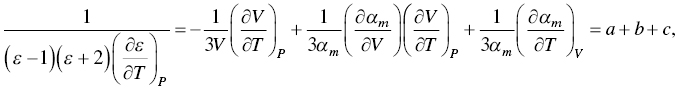
where:
- a: when the temperature increases, the specific volume will increase, the inter‐atomic spacing will also increase and the dielectric constant will decrease with constant pressure;
- b: when the volume of the lattice will increase, the polarizability of the macroscopic sphere increases;
- c: it decides how polarizability changes with the temperature when the volume is constant [6].
1.4.2 Realization of Thermo‐Optical Switches
The first realized thermo‐optical switch is a digital optical switch (DOS). It is useful for space switching systems where multiple wavelength operation is needed. The operating principle of DOS is based on the waveguide heating process. A Y‐shaped junction is placed on the substrate integrated core‐cladding stack. Two electrodes are deposited on the two arms of the Y‐shaped junction. The refractive index has been varied by heating one single arm at a time or heating both arms at the same time. Improved functionalized DOS has been reported in several literatures [17].
1.4.3 Thermo‐Optical Switch Materials and Applications
The thermo‐optical switch can be implemented from specific materials which have low optical losses, low polarization‐dependent losses, low wavelength dispersion, resistance to humidity, mechanical properties with thermal stability, etc. Polymeric materials, benzocyclobutene, fluoroacrylate, polyimide, polyurethane, amorphous silica, silicon, silicon nanocrystals, III‐V semiconductors, lithium niobate (LiNbO3), tantalum pentoxide (Ta2O5), and aluminum oxide (A12O3) have been used for the production of the thermo‐optical switches [6]. Recently, the photonic crystal‐based thermo‐optical switch has also been reported [18].
1.5 Liquid Crystal‐Optical Switching
Liquid crystal bears two opposite meanings words in its nomenclature. This is because they exhibit intermediate phases in which the state of the matter shows characteristics like liquids as well as crystals [8]. The phase of the liquid crystal is represented in terms of ‘nematic’ in electro‐optical applications. The tensor of the refractive index of nematic is presented similarly to the dielectric tensor of a material.
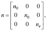
where ne stands for the extraordinary index of refraction, and n0 is the ordinary index of refraction. The birefringence of a nematic liquid crystal can be defined as ∆n = ne − n0. The values possible for ∆n reside between 0.01 and 0.3. This large range of values of ∆n coupled with the rotation of molecules of the liquid crystal helps in the polarization of light in optical communication systems. The refractive index of the extraordinary ray is given by (1.11) [19, 20].
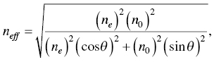
where θ is the angle between the propagation vector of the extraordinary ray and the director axis [21].
1.5.1 Types of Liquid Crystal‐Optical Switches
In liquid crystals, the refractive index and birefringence are calculated from the arrangement of the molecules, which further helps in the formation of the switches for the optical communication systems. The arrangement of the molecules in liquid crystals can be controlled by applying an electric field across the liquid crystal.
(a) Liquid Crystal Optical Switch Based on Birefringence: These types of switches are made by controlling the direction of the light propagation along the liquid crystals to modify the birefringence property of the medium without changing the polarization state, but controlling the reflection and refraction of light coming out of the surface. A setup of this type of liquid crystal switch has been presented in Figure 1.3. The refractive index of the liquid crystal (LC) molecules can be monitored by placing them accordingly the light propagation vector through the LC material. The change in refractive index in different cases causes transmission of the optical beam or total internal reflection (TIR) of the optical beam [22].

Figure 1.3 States of liquid crystal for transmission and total internal reflection (TIR).
Two other important types of liquid crystal optical switches are (b) liquid crystal optical switch based on polarization and (c) wavelength‐selective liquid crystal optical switch.
1.5.2 Liquid Crystal‐Optical Switch Applications
Liquid crystal‐based switches offer vast use in telecommunication applications because they need shorter response time and larger efficient optical networks. Modern‐day displays called LCD are in use everywhere. LCD technology eradicates the demerits of temperature dependence, power consumption, etc. Liquid crystal optical switches find applications in beam steering applications. In the photonics domain, liquid crystal optical switches have been used as photonic crystal fiber (PCF) [23]. Liquid crystal optical switches are used to achieve polarization diversity features in smart antenna applications to set different focal points from the same system [24]. They have been used in logic devices also [25]. These types of switches have also been used in polarization switching applications in communication systems.
1.6 Photonic Crystal Optical Switching
Most optical switches operate on the principle of refractive index change or phase shift between the two ports [8]. An optical switching occurs when the phase difference of the light between the two ports becomes π, corresponding to the path difference of λ/2. The change in refractive index is very small in most of the all‐optical switches. Therefore, a very long path length device is needed for making the required phase shift. Due to large light‐matter interaction and bandgap property, photonic crystal‐based optical switches have the advantage of smaller size devices and higher integration [26].
Photonic crystals are the periodic arrangement of the dielectric rod or air hole perforated in a dielectric slab to manipulate the light within a crystal platform. Depending on the periodicity direction, photonic crystals are classified as one‐dimensional (1D PCs), two‐dimensional (2D PCs), and three‐dimensional (3D PCs) [27]. Photonic crystals can be arranged in a square or triangular lattice. It prohibits/guides the light in a certain defined range of frequency called bandgap which is obtained from the dispersion diagram of the unit cell of the periodic structure. The bandgap of the periodic structure can be controlled by varying the dimensions of the periodic unit cells and the refractive index difference of the substrate and surrounding material. Due to ease in fabrication, mostly two‐dimensional photonic crystals are used for the optical switches [28–31]. All‐optical switch in 2D PCs can be realized by introducing one of the following in PCs:
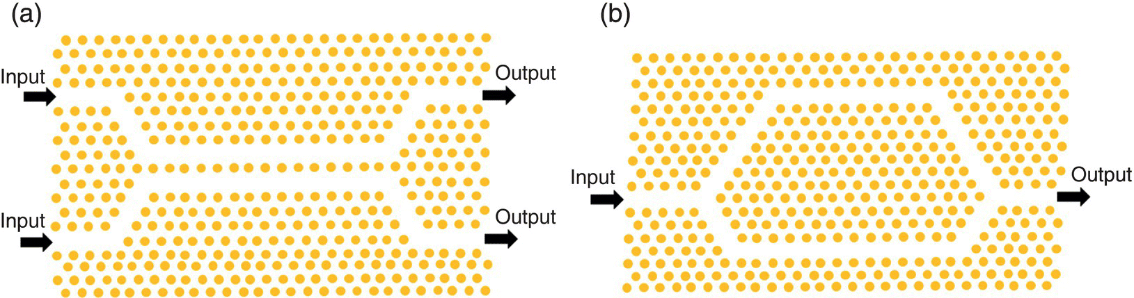
Figure 1.4 Realization of (a) directional coupler, and (b) Mach–Zehnder interferometers from photonic crystal.
- directional coupler structures [32–34],
- Mach–Zehnder interferometer [35–37], and
- resonators [38–41].
Directional coupler photonic crystal can be realized by introducing the line defect waveguide, i.e., removing a row of the dielectric rod or air hole in the dielectric slab from photonic crystals which create a waveguide to guide the electromagnetic wave. Figure 1.4(a) shows two‐line defect waveguides separated by a row of rods [34]. An electromagnetic wave, launched in one waveguide, is coupled or switched to other waveguides under suitable conditions.
Mach–Zehnder interferometers (MZIs) as an optical switch in photonic crystals can be implemented by making the difference in the effective path lengths between two optical signals, which results in a difference of phase shift. In MZIs, when an optical signal enters the photonic crystal, it splits into two different optical signals and propagates through each arm of the MZI as shown in Figure 1.4(b) [37]. A phase shift between the two optical signals occurred due to the difference in the path length. When these two signals are further added, depending on the phase shift, the signal intensity at the output is either high or low and therefore acts as a switch.
Due to the long device length in the directional coupler and MZI structure, they are difficult to integrate with the other optical components [42]. By using the resonator‐based photonic crystal, the size of the optical switch can be reduced efficiently.
Resonator‐based photonic crystals have nanocavities that restrict the light in a very small region that results in higher interaction of light with matter and reduction in size. To design the multiport optical switch, either square‐shaped [38] or circular‐shaped resonators [28] with waveguide structure are mostly used. The schematic of the photonic crystal with square‐ and circular‐shaped resonator are shown in Figure 1.5. When the optical signal enters in photonic crystal waveguide, the refractive index of the material in the cavity changed which shifts the resonance frequency, and switching occurs at the output.
1.7 Semiconductor Optical Amplifier (SOA) Optical Switching
Semiconductor optical amplifier (SOA) based all‐optical switches have multi‐fold advantages: compact size, mass production, low switching power, larger nonlinear coefficients, and low latency due to monolithic integration [43]. A schematic of the SOA is shown in Figure 1.6, which is used for amplification of optical signal based on the gain of the semiconductor medium. The principle of SOA is similar to that of a laser diode where light is amplified by stimulated emission [44]. But in the structure, the mirrors at both the facets of the laser are replaced by antireflection coatings to eliminate the resonator structure. In addition, to reduce the reflectance at the end, an inclined waveguide can also be used.

Figure 1.5 Photonic crystal switching by: (a) square‐shaped and (b) circular‐shaped ring resonator.
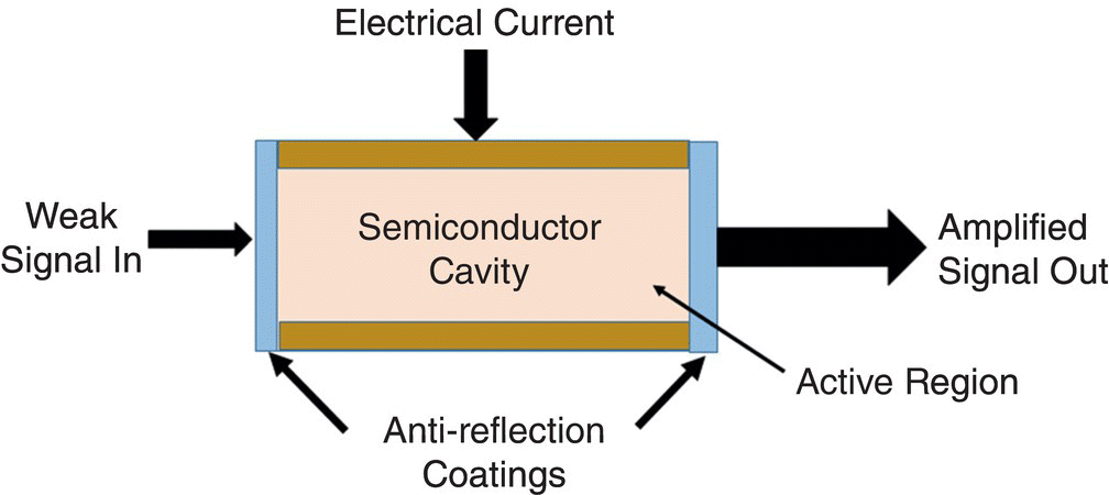
Figure 1.6 Schematic of SOA.
In SOA, weak signal input is passed through the single‐mode waveguide, which has significant overlap with the active region. An electric current is used to drive the active region of the SOA, which generates the large carrier density in the conduction band. These generated carriers take part in the optical transition from the conduction band to the valence band.
SOAs can be categories into two types [45]:
- Fabry–Pérot Amplifiers (FPA)
In FP amplifiers, due to mirrors at the facets, light is reflected back to the active region and acts as a resonant cavity. Therefore, the light gets amplified due to reflection between the two facets. FPA is sensitive to the frequency of the input signal and temperature.
- Traveling‐Wave Amplifiers (TWA)
In contrast to FPA, TWA has antireflection coatings at the facets. Therefore, multiple reflections in the active region do not take place for TWA, and input light gets amplified in a single pass through the amplifier. TWA is widely used due to its large bandwidth and low polarization sensitivity.
SOA‐based optical switches can be made by integrating SOA with gating elements. The switching function can be achieved by making the gating element sensitive to the property changed by the SOA, like wavelength, phase, and amplitude.
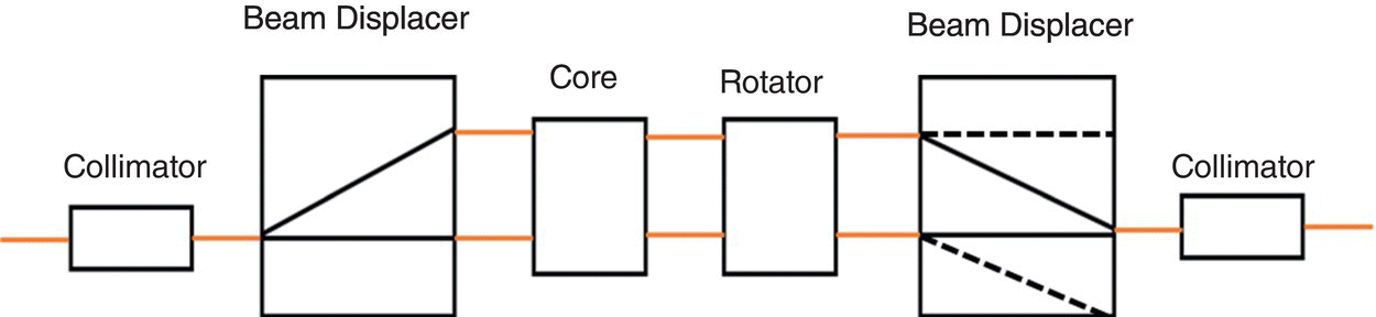
Figure 1.7 Working of MO switch.
1.8 Magneto‐Optical (MO) Optical Switching
All‐optical switches, e.g., MEMS switches, thermo‐optic switches, and electro‐optic switches, have high insertion loss or low switching speed. To overcome these limitations a magneto‐optical (MO) switch has been developed which has low insertion loss and fast switching time. The magneto‐optical switch worked on the principle of Faraday rotation of polarized light. By changing the external magnetic field, the polarization of the incident polarized light changed, thus switching the optical path [46–48].
Generally, the MO switch is composed of beam displacer, core, and Faraday rotator, as shown in Figure 1.7. The working principle of MO switch is as follows: When the light has been passed through the collimator and entered into the beam displacer, light is divided into mutual orthogonal polarization. Then, by changing the external magnetic field, the rotator changes the polarization plane of incidence polarized light, and thus the light route is switched.
Optical switches with MO materials have several advantages, which include high integration, low insertion loss, large optical cross‐section, low operating voltage, polarization‐independence, and non‐reciprocity of the induced rotation. Further, due to no physical movement, MO switch has better reliability.
1.9 Micro Electro‐Mechanical Systems (MEMS) Optical Switching
A system that consists of micrometer‐sized electrical and mechanical components called MEMS and its applications include actuators, accelerometers, sensors, switches, and gyroscopes [49–51]. The MEMS system is fabricated by photolithography, ion beam etching, chemical etching, wafer bonding, etc.
The structure of the MEMS‐based optical switch is shown in Figure 1.8. It consists of an array of a small mirror on the silicon crystal. The array of the mirror is driven by electromagnetic or electrostatic force to switch the direction of the input light. When the light is passed through the input collimator array towards the mirror array, the angle of the mirror is changed by the driven force. Thus, the input light changes its path to the different output terminals of the optical switch to realize the ON and OFF function of the light path. In general, MEMS‐based optical switches are categories into two types based on spatial structure: 2D switches and 3D switches as shown in Figure 1.8 [49].
By using micromechanical manufacturing technology, the mirror array of the 2D MEMS optical switch is integrated on the silicon substrate. Mirrors in the array have CROSS and BAR states as shown in Figure 1.8(a). Input light is reflected to the output collimator by using CROSS state mirrors, while input light passes through uninterrupted from the mirror array by using BAR state mirror.

Figure 1.8 MEMS‐based optical switch (a) 2D, and (b) 3D.
Source: [49]/IEEE.
In the 3D MEMS optical switch, the micro‐mirror can rotate along two axes which results in the multiple positions of each mirror and direct light to multiple angles (changing the optical path) as shown in Figure 1.8(b). 3D MEMS switch contains pair of mirror arrays: input mirror and output mirror. The input light first reaches the array of input mirror, then reflected towards output mirror array, and finally reflected to the output collimator array.
The MEMS optical switches are widely used due to their advantages of high integration, low power consumption, and low cost.
1.10 Metasurfaces Switches
Metasurfaces are normally used to manipulate the electromagnetic wave or light. Metasurfaces have a diverse field of applications in light absorbers, polarization converters, phase shifters, cloaking, and filters, etc. [52–56]. Recently, lumped elements have been incorporated with the metasurfaces to achieve switching characteristics. Most of the developments have been made for the microwave and milimeter wave domain [57, 58]. Graphene has also been used as a switch in a recent literature for terahertz applications [59]. Metasurfaces‐based switching applications for the optical domain have not been explored explicitly.
1.11 Conclusion
Optical switches are one of the most important devices for enhancing the transmission rate and bandwidth and reducing the network cost in optical communication systems. An overview of various types of optical switching has been discussed in this chapter. The electro‐optic switches are advantageous for their tiny size due to single mode of operation and are independent on polarization of the input signal. In acoustic switches, change in refractive index occurred by acoustic wave but has the disadvantage of low sensitivity, poor response to optical signal, and high crosstalk. The optical switches based on thermo‐optic effect has been mostly fabricated by silicon‐on‐insulator (SOI) technology due to its larger thermo‐optic coefficient. These switches consume less power and have fast response for the optical signal. Photonic crystal switches based on nonlinear material have ultra‐high response due to the fast response of nonlinear material. Due to the small size of the photonic crystals, these switches are easy to integrate with future high‐speed optical networks. However, higher coupling of these switches with optical fiber is still challenging. Magneto‐optic switches utilize the Faraday rotation for the switching application. These switches have the advantages of higher integration, low insertion loss, large optical cross‐section, low operating voltage, and polarization‐independence. But the area for the suitable materials for magneto‐optic switches needs more research. Finally, MEMS switches have been discussed which offer several advantages like high integration, low power consumption, and low cost. These switches are most widely used optical switches. MEMS architectures with 2D and 3D structure have been described. Metasurface‐based optical switches are in the embryonic stage and need to be further explored.
Bibliography
- 1 G.I. Papadimitriou, C. Papazoglou, and A.S. Pomportsis. Optical Switching. Wiley‐Interscience, 2006.
- 2 V. Sasikala and K. Chitra. All optical switching and associated technologies: a review. Journal of Optics, 47(3):307–317, 2018.
- 3 F. Lecocq, F. Quinlan, K. Cicak, J. Aumentado, S.A. Diddams, and J.D. Teufel. Control and readout of a superconducting qubit using a photonic link. Nature, 591(7851):575–579, 2021.
- 4 C.Y. Jin and O. Wada. Photonic switching devices based on semiconductor nano‐structures. Journal of Physics D: Applied Physics, 47(13):133001, 2014.
- 5 P. Andreakou, S.V. Poltavtsev, J.R. Leonard, E.V. Calman, M. Remeika, Y.Y. Kuznetsova, L.V. Butov, J. Wilkes, M. Hanson, and A.C. Gossard. Optically controlled excitonic transistor. Applied Physics Letters, 104(9):091101, 2014.
- 6 S.J. Chua and B. Li, eds. Optical Switches: Materials and Design. Elsevier, 2010.
- 7 J.K. Song. Electro‐optical switching of liquid crystals of graphene oxide. In Liquid Crystals with Nano and Microparticles (pp. 817–846), 2017.
- 8 T.S. El‐Bawab. Optical Switching. Springer Science & Business Media, 2006.
- 9 A. Yariv and P. Yeh. Optical Waves in Crystals (Vol. 5). New York, Wiley, 1984.
- 10 C.S. Tsai. Guided‐Wave Acousto‐Optics. Springer‐Verlag, 1990.
- 11 H. Nishihara, M. Haruna, and T. Suhara. Optical Integrated Circuits. McGraw‐Hill, 1989.
- 12 J.Y Son, S.A. Shestak, V.M. Epikhin, J.H. Chun, and S.K. Kim. Multichannel acousto‐optic Bragg cell for real‐time electroholography. Applied Optics, 38(14):3101–3104, 1999.
- 13 J. Blanche Pierre‐Alexandre. Field Guide to Holography. SPIE, 2014.
- 14 R.S. Weis and T.K. Gaylord. Lithium niobate: summary of physical properties and crystal structure. Applied Physics A, 37(4):191–203, 1985.
- 15 N.W. Ashcroft and N.D. Mermin. Solid State Physics. New York, London, Holt, Rinehart and Winston, 1976.
- 16 P.Y. Yu and M. Cardona, Fundamentals of Semiconductors; Physics and Materials Properties. Berlin and Heidelberg, Springer‐Verlag, 1996.
- 17 Y.T. Han, J.U. Shin, S.H. Park, S.P. Han, C.H. Lee, Y.O. Noh, H.J. Lee, and Y. Baek. Crosstalk‐Enhanced DOS Integrated with Modified Radiation‐Type Attenuators. ETRI Journal, 30(5):744–746, 2008.
- 18 K. Cui, Q. Zhao, X. Feng, Y. Huang, Y. Li, D. Wang, and W. Zhang. Thermo‐optic switch based on transmission‐dip shifting in a double‐slot photonic crystal waveguide. Applied Physics Letters, 100(20):201102, 2012.
- 19 P.G. de Gennes. The Physics of Liquid Crystals. Oxford, Clarendon Press, 1974.
- 20 S. Chandrasekhar. Liquid Crystals (2nd ed.). Cambridge, Cambridge University Press, 1992.
- 21 J.C. Chiao, K.Y. Wu, and J.Y. Liu, September. Liquid‐crystal WDM optical signal processors. In 2001 IEEE Emerging Technologies Symposium on BroadBand Communications for the Internet Era. Symposium Digest (Cat. No. 01EX508), 53–57, 2001.
- 22 K. Noguchi, T. Sakano, and T. Matsumoto. A rearrangeable multichannel free‐space optical switch based on multistage network configuration. Journal of Lightwave Technology, 9(12):1726–1732, 1991.
- 23 K.R. Khan, S. Bidnyk, and T.J. Hall. Tunable all optical switch implemented in a liquid crystal filled dual‐core photonic crystal fiber. Progress in Electromagnetics Research, 22, 179–189, 2012.
- 24 Y. Sakamaki, K. Shikama, Y. Ikuma, and K. Suzuki. Wavelength selective switch array employing silica‐based waveguide frontend with integrated polarization diversity optics. Optics Express, 25(17):19946–19954, 2017.
- 25 K. Asakawa, Y. Sugimoto, Y. Watanabe, N. Ozaki, A. Mizutani, Y. Takata, Y. Kitagawa, H. Ishikawa, N. Ikeda, K. Awazu, and X. Wang. Photonic crystal and quantum dot technologies for all‐optical switch and logic device. New Journal of Physics, 8(9):208, 2006.
- 26 D.M. Beggs, T.P. White, L. O'Faolain, and T.F. Krauss. Ultracompact and low‐power optical switch based on silicon photonic crystals. Optics Letters, 33(2):147–149, 2008.
- 27 J.D. Joannopoulos, S.G. Johnson, J.N. Winn, and R.D. Meade. Photonic Crystals. Princeton University Press, 2011.
- 28 R. Rajasekar, K. Parameshwari, and S. Robinson. Nano‐optical switch based on photonic crystal ring resonator. Plasmonics, 14(6):1687–1697, 2019.
- 29 Y. Zhang, P. Li, Y. Chen, and Y. Han. Four‐channel THz wave routing switch based on magneto photonic crystals. Optik, 181, 134–139, 2019.
- 30 L. O'Faolain, D.M. Beggs, T.P. White, T. Kampfrath, K. Kuipers, and T.F. Krauss. Compact optical switches and modulators based on dispersion engineered photonic crystals. IEEE Photonics Journal, 2(3):404–414, 2010.
- 31 M. Djavid, M.H.T. Dastjerdi, M.R. Philip, D.D. Choudhary, T.T. Pham, A. Khreishah, and H.P.T. Nguyen. Photonic crystal‐based permutation switch for optical networks. Photonic Network Communications, 35(1):90–96, 2018.
- 32 C.C. Chen, C.Y. Chen, W.K. Wang, F.H. Huang, C.K. Lin, W.Y. Chiu, and Y.J. Chan. Photonic crystal directional couplers formed by InAlGaAs nano‐rods. Optics Express, 13(1):38–43, 2005.
- 33 F. Cuesta‐Soto, A. Martínez, J. Garcia, F. Ramos, P. Sanchis, J. Blasco, and J. Martí. All‐optical switching structure based on a photonic crystal directional coupler. Optics Express, 12(1):161–167, 2004.
- 34 A. Granpayeh, H. Habibiyan, and P. Parvin. Photonic crystal directional coupler for all‐optical switching, tunable multi/demultiplexing and beam splitting applications. Journal of Modern Optics, 66(4):359–366, 2019.
- 35 A. Martínez, P. Sanchis, and J. Martí. Mach–Zehnder interferometers in photonic crystals. Optical and Quantum Electronics, 37(1):77–93, 2005.
- 36 H.C. Nguyen, S. Hashimoto, M. Shinkawa, and T. Baba. Compact and fast photonic crystal silicon optical modulators. Optics Express, 20(20):22465–22474, 2012.
- 37 C.Y. Liu and L.W. Chen. Tunable photonic‐crystal waveguide Mach–Zehnder interferometer achieved by nematic liquid‐crystal phase modulation. Optics Express, 12(12):2616–2624, 2004.
- 38 M. Shirdel and M.A. Mansouri‐Birjandi. Photonic crystal all‐optical switch based on a nonlinear cavity. Optik, 127(8):3955–3958, 2016.
- 39 J. Bravo‐Abad, A. Rodriguez, P. Bermel, S.G. Johnson, J.D. Joannopoulos, and M. Soljačić. Enhanced nonlinear optics in photonic‐crystal microcavities. Optics Express, 15(24):16161–16176, 2007.
- 40 M. Ghadrdan and M.A. Mansouri‐Birjandi. Concurrent implementation of all‐optical half‐adder and AND & XOR logic gates based on nonlinear photonic crystal. Optical and Quantum Electronics, 45(10):1027–1036, 2013.
- 41 V.D. Kumar, T. Srinivas, and A. Selvarajan. Investigation of ring resonators in photonic crystal circuits. Photonics and Nanostructures‐Fundamentals and Applications, 2(3):199–206, 2004.
- 42 D.A. Miller. Device requirements for optical interconnects to silicon chips. Proceedings of the IEEE, 97(7):1166–1185, 2009.
- 43 R. Konoike, K. Suzuki, T. Inoue, T. Matsumoto, T. Kurahashi, A. Uetake, K. Takabayashi, S. Akiyama, S. Sekiguchi, S. Namiki, and H. Kawashima. SOA‐integrated silicon photonics switch and its lossless multistage transmission of high‐capacity WDM signals. Journal of Lightwave Technology, 37(1):123–130, 2018.
- 44 H. Ghafouri‐Shiraz. Principles of Semiconductor Laser Diodes and Amplifiers: Analysis and Transmission Line Laser Modeling. World Scientific, 2003.
- 45 G. Keiser. Optical fiber communications. Wiley Encyclopedia of Telecommunications, 2003.
- 46 R. Bahuguna, M. Mina, J.W. Tioh, and R.J. Weber. Magneto‐optic‐based fiber switch for optical communications. IEEE Transactions on Magnetics, 42(10):3099–3101, 2006.
- 47 S. Kemmet, M. Mina, and R.J. Weber. Current‐controlled, high‐speed magneto‐optic switching. IEEE Transactions on Magnetics, 46(6):1829–1831, 2010.
- 48 T. Murai, Y. Shoji, N. Nishiyama, and T. Mizumoto. Nonvolatile magneto‐optical switches integrated with a magnet stripe array. Optics Express, 28(21):31675–31685, 2020.
- 49 M. Džanko, B. Mikac, and V. Miletić. Availability of all‐optical switching fabrics used in optical cross‐connects. In 2012 Proceedings of the 35th International Convention MIPRO, 568–572, 2012.
- 50 G.I. Papadimitriou, C. Papazoglou, and A.S. Pomportsis. Optical switching: switch fabrics, techniques, and architectures. Journal of Lightwave Technology, 21(2):384, 2003.
- 51 P. De Dobbelaere, K. Falta, and S. Gloeckner. Advances in integrated 2D MEMS‐based solutions for optical network applications. IEEE Communications Magazine, 41(5):pp.S16–S23, 2003.
- 52 S.K. Ghosh, V.S. Yadav, S. Das, and S. Bhattacharyya. Tunable graphene‐based metasurface for polarization‐independent broadband absorption in lower mid‐infrared (MIR) range. IEEE Transactions on Electromagnetic Compatibility, 62(2):346–354, 2019.
- 53 S.K. Ghosh, S. Das, and S. Bhattacharyya. Graphene based metasurface with near unity broadband absorption in the terahertz gap. International Journal of RF and Microwave Computer‐Aided Engineering, 30(12):e22436, 2020.
- 54 V.S. Yadav, S.K. Ghosh, S. Das, and S. Bhattacharyya. Wideband tunable mid‐infrared cross‐polarisation converter using monolayered graphene‐based metasurface over a wide angle of incidence. IET Microwaves, Antennas & Propagation, 13(1):82–87, 2019.
- 55 V.S. Yadav, S.K. Ghosh, S. Bhattacharyya, and S. Das. Graphene‐based metasurface for a tunable broadband terahertz cross‐polarization converter over a wide angle of incidence. Applied Optics, 57(29):8720–8726, 2018.
- 56 S.K. Ghosh, S. Das, and S. Bhattacharyya. Transmittive‐type triple‐band linear to circular polarization conversion in THz region using graphene‐based metasurface. Optics Communications, 480, 126480, 2021.
- 57 R. Phon, S. Ghosh, and S. Lim. Novel multifunctional reconfigurable active frequency selective surface. IEEE Transactions on Antennas and Propagation, 67(3):1709–1718, 2018.
- 58 S. Ghosh and K.V. Srivastava. A polarization‐independent broadband multilayer switchable absorber using active frequency selective surface. IEEE Antennas and Wireless Propagation Letters, 16, 3147–3150, 2017.
- 59 P. Kumar, S. Rai, S. Bhattacharyya, and A. Lakhtakia. Graphene‐sandwich metasurface as a frequency shifter, switch, and isolator at terahertz frequencies. Optical Engineering, 59(11):110501, 2020.