
2
Electro‐Optic Switches
Arpita Adhikari1, Joydip Sengupta2, and Arijit De3
1 Department of Electronics and Communication Engineering, Techno Main Salt Lake, Kolkata, West Bengal, India
2 Department of Electronic Science, Jogesh Chandra Chaudhuri College, Kolkata, West Bengal, India
3 Department of Electronics and Communication Engineering, Netaji Subhash Engineering College, Kolkata, West Bengal, India (Presently associated with CNES/ ONERA project)
2.1 Introduction
Superfast transmission of large data sets is now needed to cope with the increasing demand for high‐quality audio and video signals in mobile phones, smart TV etc. [1]. Currently, the advanced fiber‐optic communication networks serve as the building blocks of the information superhighway. Reliable routing, fast switching, and errorless detection are the three essential goals that need to be fulfilled to accommodate the huge demands within the purview of fiber‐optic communication technology. One of the indispensable components of fiber‐optic communication is optical switches and, for the current scenario, they need to be reliable, robust, yet inexpensive. A good‐quality optical switch can increase the capacity of optical fiber and reliably distribute optical signals and subsequently reduces the overall cost. Moreover, optical switches can convert or redirect light without any electronic to optical conversions and vice versa. In the electro‐optic effect, the refractive index (RI) of non‐centrosymmetric crystals can be changed upon application of an electric field due to the rearrangement of the position and/or density of the charge carriers and by inducing slight deformations in the crystal lattice. There are two categories of electro‐optic effect, namely the linear (Pockels) effect (RI varies in proportion to the field) and the quadratic (Kerr) effect (RI varies in proportion to the square of the field). Electro‐optic modulation has distinct advantages over the other mechanisms that can be used for 1.31–1.55 μm fiber‐optic communications and optical networks. Moreover, light can be restrained within a tiny area by using guided‐wave‐type electro‐optic modulators, which are much superior to their conventional bulk counterparts in terms of switching speed, power consumption, and compatibility with optical fiber [2]. Thus, an electro‐optic modulator‐based efficient optical communication system is evidently required for telecommunication, remote detection systems [3], military applications, etc. In this article, a review of current optical switches in terms of operating principle, fabrication material, and device structure is presented. The performance issues and subsequent challenges are also briefly discussed.
2.2 Operating Principles
2.2.1 Operating Principles of the Single‐Mode Switch
The fundamental building block of the optical switch is known as the ridge waveguide [4]. The parting between the cut‐off numbers of the dominant and first higher‐order mode of a ridge waveguide is much larger in comparison to that for a conventional rectangular waveguide. Structurally, if one or two ridges are inserted in the top or bottom or both of the walls of the rectangular waveguide, then it becomes a ridge waveguide (Figure 2.1). In a ridge waveguide, the cut‐off number can be altered by amending the dimensions of the ridge without modifying the outside dimensions. Moreover, the characteristic impedance value of the ridge waveguide can be varied in such a way that it lies in between that of a regular rectangular waveguide and coaxial cable. From the design perspective, the numerical aperture (NA) of the ridge waveguide must be matched with that of single‐mode fiber. Secondly, the cross‐section of the ridge waveguide must be enough wide to accommodate the core of the single‐mode fiber. Considering the points discussed above, a ridge waveguide can be principally operated as a single‐mode switch.
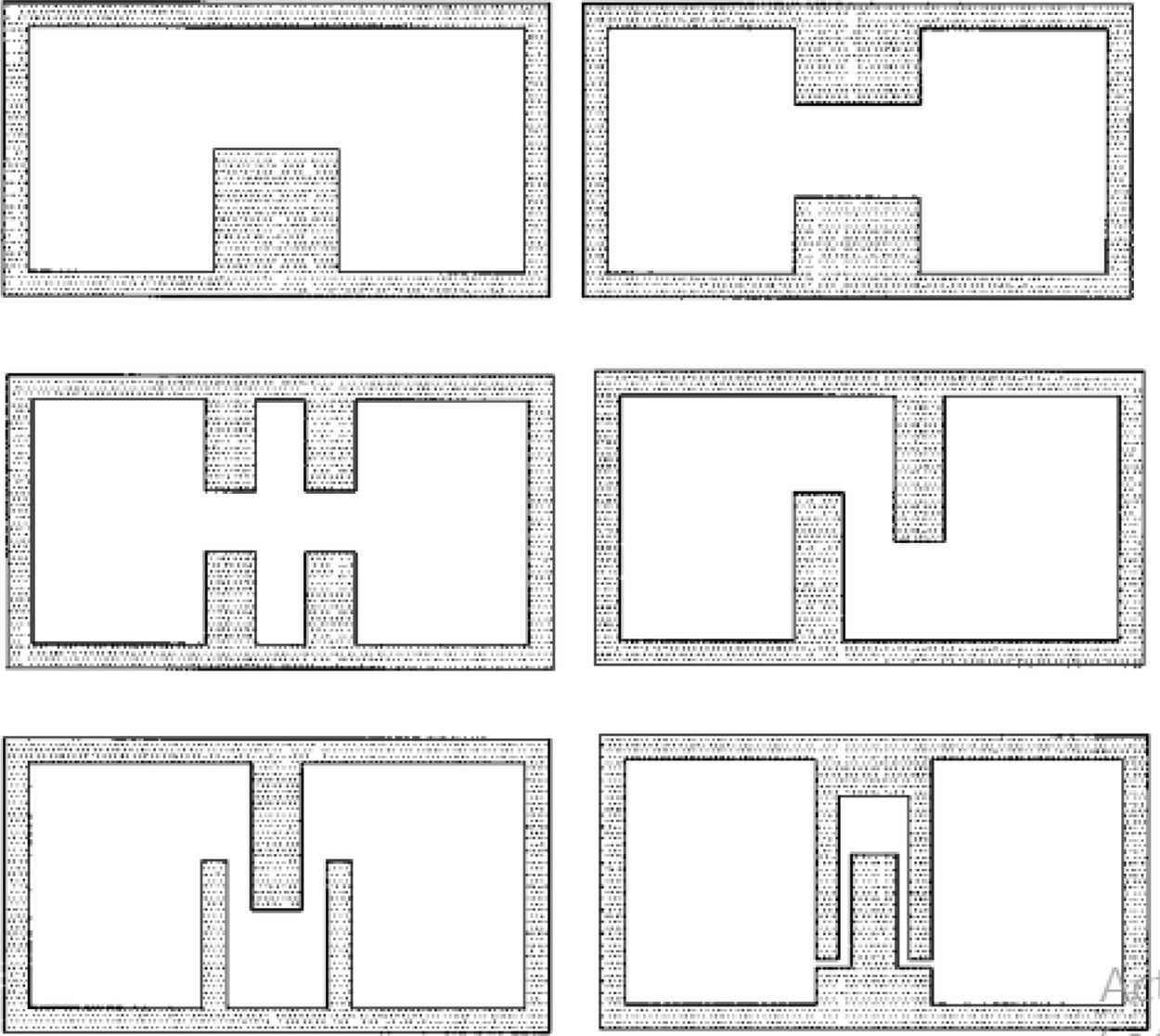
Figure 2.1 Schematic diagrams of rectangular ridge waveguides.
Source: [5]/IET.
2.2.2 Operating Principles of the Multimode Switch
Recently, optical switches based on multimode interference (MMI) [6] have gained global attention because of their novel characteristics, such as low loss, compactness, polarization insensitivity, simple design, ease of fabrication, and large optical bandwidth. The self‐imaging principle is the primary theory on which the optical MMI switch is operated. The self‐imaging principle was first reported nearly 200 years ago [7]. The principle was beautifully described in Soldano’s article [8]: “Self‐imaging is a property of multimode waveguides by which an input field profile is reproduced in single or multiple images at periodic intervals along the propagation direction of the guide”. The pictorial representation of the self‐imaging principle is shown in Figure 2.2.
Structurally, an MMI device is a waveguide that is designed in such a way that it is capable of facilitating lots of modes (typically ≥ 3). More than one waveguide is positioned at the beginning and the end of the MMI device for launching light into it and recovering light from it. These types of devices are designated as N × M MMI couplers, where N and M are the numbers of input and output waveguides, respectively (Figure 2.3).

Figure 2.2 Field distribution of MMI.
Source: [9]/SPIE.

Figure 2.3 Optical micrographs of (a) a 3 × 3 MMI coupler electro‐optic switch device, (b) electrode contact pads A and B deposited on the two index‐modulated regions, including two extended square metal pads for easy contact, and (c) a top view of the MMI and coupling waveguide parts. Scanning electron microscope images of the cross‐section of (d) a ridge input (output) waveguide, and (e) an MMI waveguide.
Source: [10]/Optica Publishing Group.
2.3 Materials for the Fabrication of Electro‐Optic Switch
2.3.1 Ferroelectric Materials
Several ferroelectric materials such as lead zirconate titanate – Pb(Zr, Ti)O3 or PZT [11] – lead lanthanum zirconate titanate – (Pb, La)(Zr, Ti)O3 or PLZT [12] – and lithium niobate (LiNbO3) [13] are used for the fabrication of electro‐optic switches. However, due to the large electro‐optic coefficient [14], LiNbO3 is widely used for the fabrication of electro‐optic switches, demonstrating the Pockels effect with typical RI value 2.2 [15]. LiNbO3 crystal possesses electric dipoles even in the absence of an electric field. Another advantage of LiNbO3 is that it is capable of modifying the intensity of light without any perturbation on the phase, which is an important requirement for high‐bitrate optical signals. Czochralski’s (CZ) process is generally used to grow LiNbO3 and as the CZ process is a matured technology high‐quality LiNbO3 is readily available in the market. In addition, the physical properties of LiNbO3 are in line with the cleanroom process. The high Curie temperature [16] of LiNbO3 maintains the electro‐optic properties during high‐temperature annealing. Since the LiNbO3 crystal is anisotropic, the RI for light polarized along the c‐axis (Figure 2.4) is thus smaller than that in the perpendicular direction to the c‐axis. Moreover, the RI in the directions normal to the c‐axis has strongly influenced the composition of the LiNbO3, the operating temperature, and the wavelength used, rather than those along the c‐axis. LiNbO3 also possesses a wide transparency band [17] with low dispersion loss [18], which offers a wide range of applications from visible to mid‐infrared region. Thus LiNbO3 is employed widely for its ever‐lower propagation losses and minor coupling losses with fibers, low power consumption, and very fast switching speeds while maintaining ever higher electro‐optic efficiency.
![Schematic illustration of crystal structure of LiNbO3 [19].](https://imgdetail.ebookreading.net/2023/10/9781119819233/9781119819233__9781119819233__files__images__c02f004.gif)
Figure 2.4 Crystal structure of LiNbO3 [19].
2.3.2 Compound Semiconductors
Compound semiconductors possess a linear electro‐optic coefficient, though it is much smaller in comparison to that of LiNbO3. However, a high RI value (typically 3.5 [20]) compared to LiNbO3 compensates for a lower electro‐optic coefficient. The RI can be controlled either by the introduction of an electric field or the injection of carriers. Moreover, in compound semiconductors, because of the dispersion of the dielectric constant, a much larger electric field can be employed for the same applied voltage, which in turn significantly increases the modulation efficiency. The dependence of the dielectric constant on the frequency of the applied signal is also much less in the case of compound semiconductors. Moreover, quadratic electro‐optic effects can be used for enhancing the electro‐optic efficiency of compound semiconductors. High‐quality compound semiconductors can be grown employing metal‐organic chemical vapour deposition (MOCVD) and molecular beam epitaxy (MBE), and the resulting modulator can be potentially integrated with optical sources, detectors which are also fabricated similar technologies. Thus, it is feasible to fabricate compound semiconductor electro‐optic switches with improved drive voltage and bandwidth characteristics compared to a LiNbO3‐based electro‐optic switch, but compound semiconductor switches have higher propagation loss in comparison to LiNbO3.To date, GaAs [21], AlGaAs [22], InP [23], InGaAs [24], InAlAs [25], InGaAsP [26], or their mixed system [27] have been widely used for the fabrication of electro‐optical switches (Figure 2.5).
2.3.3 Polymers
Electro‐optic polymers contain nonlinear molecules arranged in a non‐centrosymmetric structure. The state of polarization, phase, and frequency of light beams can be controlled by varying the nonlinear optical properties of materials during fabrication. High speed, low drive in voltage, and wide bandwidth are the major factors for which electro‐optic polymers are gaining global attention [29]. Another significant aspect of electro‐optic polymers is the tunability of their RI, which facilitates high‐density compact structures. The negative thermo‐optic coefficient of electro‐optic polymers are the main factor behind low power consumption [30]. The electro‐optic coefficient of these polymers can match that of LiNbO3. Moreover, as the RI value is almost constantly low within DC to optical frequency range, the speed of the electrical and optical waves can thus be synchronized at ease [31]. The electro‐optic polymers are based on either a side‐chain system or a guest‐host system. Currently, [2] paracyclophanes are mostly used as the electro‐optic polymer for the fabrication of switches (Figure 2.6).
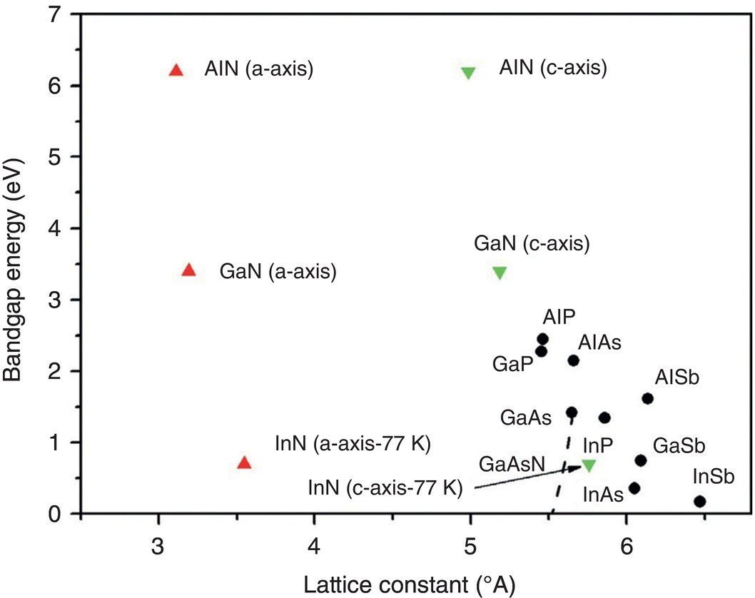
Figure 2.5 Bandgap energy (300 K) vs. lattice constant for III‐V compound semiconductors commonly used for optoelectronic devices.
Source: [28]/Elsevier.
![Schematic illustration of chemical structures of selected [2] paracyclophanes.](https://imgdetail.ebookreading.net/2023/10/9781119819233/9781119819233__9781119819233__files__images__c02f006.gif)
Figure 2.6 Chemical structures of selected [2] paracyclophanes.
Source: [32]/Taylor & Francis.
2.4 Device Structures of Electro‐Optical Switches
2.4.1 1 × 1 Switch
1 × 1 optical switch may be regarded as a 1 × 1 optical modulator. The fabrication can be done in III‐V materials as well as in LiNbO3, Si(Ge), or polymers. A single‐mode n‐type silicon waveguide of width W is formed on a SiO2 layer. The carriers are injected into the waveguide using an abrupt p+‐n junction at the forward bias condition. As a consequence, the RI decrease due to the plasma dispersion effect and the guided mode will be converted into the radiation mode. The specifications are shown in Table 2.1.
Table 2.1 Specifications for 1 × 1 optical switch.
| Switching current | Modulation depth (injection current = 45 mA) | Insertion loss (1.3 μm) | Switching time |
|---|---|---|---|
| 45 mA | 96% | 3.65 dB | 160 ns |
2.4.2 1 × 2 Switch
1×2 optical switches can be arranged as Y‐shaped waveguides. The input and output of the switch consist of one and two waveguides, respectively. A branching point having a small angle is used to connect the input to the output waveguides. This branching switch is also called digital photonic splitting (DPS). The output power of the switch is independent of the voltage variations. At a certain voltage light will be propagated through the output optical waveguide. The DPS switch has the advantages of low insertion loss, small switching voltage, minute crosstalk, high switching speed, and good reliability. A Y‐branch DPS with varied branch angles is shown in Figure 2.7. LiNbO3 substrate is used to fabricate by diffusing Ti to a depth of 60 nm and width of 7 μm at 1050°C temperature for 8 hours. The SiO2 layer has a thickness of 250 nm. The length of the electrode is 10 mm. A schematic diagram of DPS is shown in Figure 2.8. Figure 2.9 shows the configuration of the silicon 1 × 2 optical switch. Silicon single‐mode ridge waveguide is used to form a Y‐junction. An impurity induced at the n/n+ interface can be used for the vertical confinement of the optical wave whereas a Si/Si3N4 ridge wall is used for lateral confinement. The double‐etch design can be used for efficient switching and low radiation loss. A double‐etch Y‐branch switch/modulator may be designed using InGaAsP multiple‐quantum wells (MQWs). Figure 2.10 shows a configuration of a 1 × 2 digital optical switch (DOS) waveguide. Chemical beam epitaxy in InGaAsP‐InP is mainly used for the DOS p‐i‐n waveguide heterostructure. Si3N4 can be used as the insulating layer. Power consumption can be reduced by choosing a wide carrier injection region. The etching depth of the ridge waveguide is 1.2 μm with 4% of Ge content. To analyze the mode propagation behaviour, the effective index method can be used. This will help to determine the branch angle. The beam propagation method (BPM) is used to understand the device performance. In the ON condition of the switch, the 47.6% output optical power has been seen in the two arms of the Y switch. The insertion loss in this condition is 0.2 dB. The output optical powers are 58.7% and 3% at the two arms for the ON and OFF state respectively. The insertion loss in both cases is 2.1 dB. The threshold voltage and current are 1.0 V and 85 mA, respectively. The insertion loss in this condition is 3.2 dB. At 2 V forward bias voltage, the active branch is cut off. If zero and forward bias voltage are applied at branch 1 and branch 2 respectively, the output optical power at branch 1 and 2 increases and decreases respectively. The cut‐off voltage is 2 V. The injection current density and the power consumption is 6.3 kA/ cm2 and 190 mW, respectively. The measured crosstalk and the insertion loss are 29.6 dB and 5.2 dB, respectively.

Figure 2.7 Diagram of Y‐branch digital optical switch with varied local branch angle.
Source: [33]/IET.

Figure 2.8 Schematic view of the digital optical switch with epilayers.
Source: [34]/IET.

Figure 2.9 1 × 2 optical waveguide switch.
Source: [35]/IET.

Figure 2.10 (a) Configuration of the digital optical switch Y‐junction switch, and (b) effective waveguide configuration when the index under the biased electrode matches the RI of the surrounding slab region. The shaded areas indicate a high effective index, while the clear areas indicate a low effective index.
Source: [37]/IET.
2.4.3 2 × 2 Switch
The 2 × 2 Si‐based optical switches are the basic device in integrated optics. These switches are operated on the total internal reflection (TIR) principle. RI and carrier injection may control the reflection interface of the optical switch [36]. The input of the 2 × 2 SiGe waveguide is connected to the output structure of the Y branch through an intersection region.
At the top surface p‐n+ junction at forward biased condition is used to inject the carriers. This is called the carrier injection region. Because of the plasma dispersion effect in SiGe, the RI decreases in the carrier injection region. This is the reason for the formation of the region of reflection at the intersection. By adjusting the drift distance, the carrier utilization ratio can be improved. This is also called an asymmetric switch. The input light at port 1 is in the forward bias condition of the p‐n+ junction. As a consequence, the laser beam is reflected to port 3 from port 1, and the switching operation is established. Most 2 × 2 optical switches are operated based on the TIR principle. 2 × 2 switches are constructed using two single‐mode waveguides. The two waveguides intersect at an angle θ with an electrode. An optical intersecting switch with a wide deflection angle can be used to control the reflection angle [38, 39]. Two ridge waveguides can be used to form an intersectional ridge optical waveguide switch. At zero bias the input beam will propagate to port 4. At the forward bias condition, TIR occurs and the incident light beam will reflect at port 3, as a result, the switching operation is achieved. The specifications are shown in Table 2.2.
The 2 × 2 optical switches can also be worked on the principle of the free‐carrier plasma dispersion effect and the multimode interference (MMI) principle. The MMI switch is operated on the self‐imaging principle [40]. A two‐mode interference (TMI) photonic switch having a double carrier injection can be devised for application in fiber‐optic communication. In the forward bias condition, two p‐n+ junctions are used to inject. As a consequence, the injection current at both junctions increases [41]. This structure is called double carrier injection. Due to the change of RI the TMI region can be achieved. The input beam A is coupled to the single‐mode ridge waveguide 1, as designated by arrow P1 (Figure 2.11). As a consequence, mode B (fundamental mode) and C (first‐order mode) are excited. β00 and β10 are the propagation phase constants of modes B and C respectively. The above two modes may interfere along the direction of propagation. The light power at a propagation length L is given by
Table 2.2 Specifications for 2 × 2 optical switch.
| Branch angle (θ) | Bow‐tie angle (θw) | Thickness of the ridge waveguide | Width of the ridge waveguide | Etching depth | Bow‐tie electrode length is (L) | Length of the switch |
|---|---|---|---|---|---|---|
| 2° | 1.5° | 2.6 μm | 9 μm | 1.0 μm | 600 μm | 5 mm |

Figure 2.11 Schematic plan view showing the two‐mode interference photonic switch with double carrier injections output from a waveguide at forward bias.
Source: [42]/Elsevier.
and
where P3 and P4 denote the output optical power at waveguides 3 and 4, respectively. ∆ϕ denotes the phase difference between mode B and mode C and follows the condition
where ∆β = (β00 – β10).
Without forwarding bias the light will be propagated through the waveguide 3. The switch is in the OFF state. At the Forward bias condition, carriers in large numbers (I1 + I2) will be introduced into the optically modulated section. The RI in the region will decrease, which will cause the propagation constants β00 and β10 to be changed. If the following condition satisfies,
the light beam at waveguides 3 and 4 will be cut off (B1+C1 = 0). Now the switch is in the ON state. β00, β10 are the propagation constants at zero forward bias of modes B and C respectively. ∆β00 and ∆β10 are the respective changes of β00 and β10 under forward bias respectively.
2.4.4 2 × 3 Switch
2 × 2 optical switches are mainly used for multichannel switches. 2 × 3 switches are designed for multi‐ports optical switches. A 2×3 switch structure is made of three sections: input, central, and output sections. The input section is made of two waveguides (A and B) whereas the output section has three output waveguides 1, 2, and 3. The central section has an MMI waveguide with two regions I and II. These waveguides are single‐mode waveguides. Both the index‐modulation regions are designed as a p‐n junction. Under the application of forward bias to the p‐n junction RI in the regions I and II will decrease. This happens because of the plasma dispersion effect. As a consequence, the propagation constant of the optical waveguide will change. As a result, the input optical signal will be switched to the three output ports. The thickness of the ridge waveguides is 2.6 μm p‐SiGe with 4% Ge content. The MMI section will facilitate a large number of modes. If a 1.55 μm light is coupled to the input waveguide A, and if the p‐n junctions of the region I and II are at unbiased condition, then the RI will remain unchanged. The input optical signal will be propagated through the output port 3. At a particular forward bias applied to the region I, the RI decreases by 0.3. The output light will be propagated to port 1. Applying forward bias to I and II will cause the output light to switch to port 2. When a 1.55‐μm optical signal is applied to waveguide B the refractive indices will remain unchanged. The input optical signal will be propagated through port 1. Applied forward bias to the region I, will cause the output light to switch to output port 3. Application of forward bias to both the regions will cause the output light to switch to output port 2. If two similar optical signals of wavelength 1.55‐μm having the same amplitude, phase, and polarization are applied to the input A and B, they will switch to port 3 and port 1, respectively. However, when these two 1.55‐μm optical signals are applied into ports A and B with a forward bias to the region I, the output will switch to port 1 and port 3, respectively. In this condition, the switch will be at optical cross‐connection. The switch will act as an optical power combiner. The power at the output ports 1, 2, and 3 is 0.9%, 70%, and 1.0%, respectively.
2.4.5 3 × 2 Switch
Both the 3 × 2 and 2 × 3 are applied for optical combiner or cross‐connector and for multi‐wavelength [43]. It has three sections: input, central, and output. The input section consists of two S‐shaped waveguides (2 and 3) and one straight waveguide (1). The output section is made of two S‐shaped waveguides (4 and 5). The central section is the main component of the photonic switch, which is an intersecting part. The central section has two carrier injection regions that are electronically controlled. The two regions can control the flow of the optical signal between the input ports and the output ports. Mirror I and II are the two reflecting interfaces that can be triggered by forward bias voltage. Both the mirrors have an ON and OFF state. Under the application of forward bias to the carrier injection region, the carrier concentration will increase which in turn causes to reduce the RI. This causes a reflecting interface to form. This is called the mirror‐ON state. If no forward bias is applied, the RI of the material will remain unchanged. This is called a mirror‐OFF state.
The switches are designed using SiGe material. For the single‐mode operation, it has raised the ridge waveguide structure. The thickness and width are 2.5 μm and 10 μm respectively. The etching depth is 1.1±0.1 μm for a Ge content of 4%. The behaviour of the mode propagation is analyzed employing the effective index method. In the optimum design, the input and output branching angles have been chosen as 1.5° and 3° respectively. An impurity‐induced p‐SiGe/p‐Si can be used for the vertical confinement of the input light. The operation is based on the principle of TIR due to the plasma dispersion effect. The RI of SiGe is related to the carrier concentration. At forward bias condition, huge numbers of electrons are injected into the p region of the waveguide, which enhances the carrier concentration. As a consequence, a reduction in the RI of the SiGe layer can be observed. This will help to form a reflecting mirror at branch 4 or 5. The samples of the switch can be prepared using a UHV‐chemical vapor deposition (CVD) system. It has a speed of 100‐200 ns. The advantages of the device are wavelength insensitivity, polarization‐independence, single‐mode operation, ultracompact, low‐cost, and highly reliable. The applications are in photonic integrated circuits, fiber‐optic communications systems, and wavelength division multiplexed networks. The device combines multi‐wavelength coming from different input channels.
2.4.6 3 × 3 Switch
High‐capacity optical networks are required shortly for optical digital information processing. 3×3 switch or all‐optical switch combines the advantages of the MMI principle and Si‐based optical waveguide device. It is made of input, central, and output sections. The input and the output sections are made of three waveguides. The central section consists of an MMI coupler.
2.4.7 1 × 4 Switch
The 1 × 4 optical switches are mainly fabricated using InGaAsP which has been shown in Figure 2.12. It consists of a beam‐steering section and output waveguide. The beam steering section is made of a steering region and an input waveguide. The steering region is composed of two parallel layer waveguide contacts which are mainly formed by Ti/Au/Zn/Au. The two layers are separated by 22 μm. The length and width of the contact stripes are 800 μm and 10 μm respectively. The output has two waveguides. The width and length of the two waveguides are 4 μm and 500 μm respectively. At the initial condition, two waveguides are separated by 2 μm. However, the value may increase up to 5 μm. The n+‐ InP substrate is used as a wafer structure. A 1‐μm thick n‐type InP layer can be grown on 14 pairs of 10‐nm thick and undoped InGaAsP (Eg= 0.816 eV) quantum wells having interspacing of 10‐nm InGaAsP (Eg = 1.08 eV) barriers. The slab waveguide is grown using the metal‐organic chemical vapor deposition (MOCVD) technique. The principle of carrier‐induced RI change is used in the device. A laser beam of 1.51‐μm wavelength may pass through the steering region if there is no current in the contact stripes. Zinc can be diffused below the contact stripes to control the carrier spreading within. This diffused region is used to channel the electrons which enhance their efficiency. The highest carrier concentration can be seen below the stripes and the carrier concentration will be decreased with lateral distance. This will cause a graded‐index channel to form between the two stripes. The waveguide can be shifted and steer the signal beam by adjusting the ratio between the currents of the two parallel stripes. At this condition, the input beam will be directed to the output. Silicon nitride diffusion mask is used for device fabrication. The plasma‐enhanced chemical vapor deposition (PECVD) technique can be used for 200‐nm‐thick Si3N4 film deposition on the substrate surface.
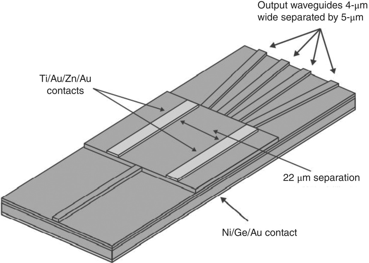
Figure 2.12 Schematic of the 1 × 4 InP‐based optical switches.
Source: [44]/Elsevier.
2.4.8 2 × 4 Switch
2 × 4 optical switches are designed based on the free‐carrier plasma dispersion effect and MMI principle. It is made of two single‐mode waveguides in the input, an MMI section, and four single‐mode waveguides in the output. Two index‐modulation regions are formed in the MMI section. When forward bias applied to the index‐modulation region, the input optical signal can be propagated to any one of the four waveguides.
The switch is made of three parts: input, central, and output section. The input and the output section consist of two and four waveguides respectively. The central section is made of a rectangular air groove and two index‐modulation regions. The p‐n junctions are formed into the index modulation. The control signals VC1 and VC 2 are the forward bias voltages. The applied control signal will decrease the RI due to the plasma dispersion effect. This phenomenon will cause an alteration in the transmission of the input signals. As a consequence, the input signals will be propagated to one of the four output waveguides. The device can be performed as a 2 × 4 decoder switch.
2.5 Conclusions
Speed, capacity, and integrability with low power consumption and errorless transmission are the key requirements of next‐generation data communication. Silicon‐based photonics extends an efficient platform in optical communication. However, the technology needs to surmount certain hurdles like controlling the optical transmission path as well as data extraction at desirable locations. The solution can be availed through the proper usage of optical switches. An optical switch in silicon‐based phonic chips extends several advantages offering state‐of‐the‐art of modern optical communication. Moreover, selective switching without intermediate conversion to an electronic counterpart is the unique feature of optical switches. Optical switches usually utilize the carrier‐induced RI modulation technique. Such switching can be either based on linear or nonlinear effects depending upon the interaction between the applied electric field and induced changes in the refractive index. Optical switching principles based on nonlinear effects are associated with high energy consumption. The carrier injection within the switching devices can either be vertical or lateral. Both modes of operation of optical switches are associated with some drawbacks. Vertical injection of carrier results in high insertion loss at the interface between the waveguide layer and n+/p+ substrate. Whereas such loss can be avoided in the case of lateral carrier injection as in that case the carriers are not necessarily transmitted through the n+/p+substrate that is utilized in the case of the vertical one for realizing ohmic contacts. However, the control of injection current or injection current density is beyond the capability of either mode of operation.
Bibliography
- 1 R. Maher, A. Alvarado, D. Lavery, and P. Bayvel. Increasing the information rates of optical communications via coded modulation: a study of transceiver performance. Scientific 6(1):21278, 2016.
- 2 J.H. Wülbern, S. Prorok, J. Hampe, A. Petrov, M. Eich, J. Luo, A. K.‐Y. Jen, M. Jenett, and A. Jacob. 40 GHz electro‐optic modulation in hybrid silicon‐organic slotted photonic crystal waveguides. Optics Letters, 35(16):2753–2755, 2010.
- 3 H. Liu, Y. Dong, R. Gao, Z. Luo, and G. Jin. Principle demonstration of the phase locking based on the electro‐optic modulator for Taiji space gravitational wave detection pathfinder mission. Optical Engineering (Redondo Beach, Calif.), 57(05):1, 2018.
- 4 S. Fattah poor, T.B. Hoang, L. Midolo, C.P. Dietrich, L.H. Li, E.H. Linfield, J.F.P. Schouwenberg, T. Xia, F.M. Pagliano, F.W.M. van Otten, and A. Fiore. Efficient coupling of single photons to ridge‐waveguide photonic integrated circuits. Applied Physics Letters, 102(13):131105, 2013.
- 5 J. Helszajn. Ridge Waveguides and Passive Microwave Components. IET, Stevenage, UK, 2000.
- 6 H. Xiao, L. Deng, G. Zhao, Z. Liu, Y. Meng, X. Guo, G. Liu, S. Liu, J. Ding, and Y. Tian. Optical mode switch based on multimode interference couplers. Journal of Optics, 19(2):025802, 2017.
- 7 H.F. Talbot. LXXVI. Facts relating to optical science. No. IV. The London and Edinburgh Philosophical Magazine and Journal of Science, 9(56):401–407, 1836.
- 8 L.B. Soldano and Pennings, E.C.M. Optical multi‐mode interference devices based on self‐imaging: principles and applications. Journal of Lightwave Technology, 13(4):615–627, 1995.
- 9 A.M. Al‐hetar. Multimode interference photonic switches. Optical Engineering (Redondo Beach, Calif.), 47(11):112001, 2008.
- 10 S. Mu, K. Liu, S. Wang, C. Zhang, B. Guan, and D. Zou. Compact InGaAsP/InP 3 × 3 multimode‐interference coupler‐based electro‐optic switch. Applied Optics, 55(7):1795–1802, 2016.
- 11 M.M. Zhu, Z.H. Du, and J. Ma. Defect enhanced optic and electro‐optic properties of lead zirconate titanate thin films. AIP Advances, 1(4):042144, 2011.
- 12 A. Mukherjee, S.R. Brueck, and A.Y. Wu. Electro‐optic effects in thin‐film lanthanum‐doped lead zirconate titanate. Optics Letters, 15(3):151–153, 1990.
- 13 H. Okayama. Lithium niobate electro‐optic switching. In Optical Switching. Springer US, Boston, MA, 39–81, 2008.
- 14 M. Luennemann, M. Luennemann, and K. Buse. Electrooptic properties of lithium niobate crystals for extremely high external electric fields. Applied Physics. B, Lasers and Optics, 76(4):403–406, 2003.
- 15 D.F. Nelson and R.M. Mikulyak. Refractive indices of congruently melting lithium niobate. Journal of Applied Physics, 45(8):3688–3689, 1974.
- 16 H. de Castilla, P. Bélanger, and R.J. Zednik. High temperature characterization of piezoelectric lithium niobate using electrochemical impedance spectroscopy resonance method. Journal of Applied Physics, 122(24):244103, 2017.
- 17 M. Leidinger, S. Fieberg, N. Waasem, F. Kühnemann, K. Buse, and I. Breunig. Comparative study on three highly sensitive absorption measurement techniques characterizing lithium niobate over its entire transparent spectral range. Optics Express, 23(17):21690–21705, 2015.
- 18 A. Chirakadze, S. Machavariani, A. Natsvlishvili, and B. Hvitia. Dispersion of the linear electro‐optic effect in lithium niobate. Journal of Physics D: Applied Physics, 23(9):1216–1218, 1990.
- 19 File:LiNbO3.png (no date) Wikimedia.org. Available at: https://commons.wikimedia.org/wiki/File:LiNbO3.png (Accessed: July 7, 2021).
- 20 D.T.F. Marple. Refractive Index of GaAs. Journal of Applied Physics, 35(4):1241–1242, 1964.
- 21 N. Dagli. Compound semiconductor electro‐optic modulators for microwave photonics applications. In 2013 IEEE Photonics Conference. IEEE, 2013.
- 22 P. Bhasker, J. Norman, J. Bowers, and N. Dagli. Low voltage, high optical power handling capable, bulk compound semiconductor electro‐optic modulators at 1550 nm. Journal of Lightwave Technology, 38(8):2308–2314, 2020.
- 23 M. Stepanenko, I. Yunusov, V. Arykov, P. Troyan, and Y. Zhidik. Multi‐parameter optimization of an InP electro‐optic modulator. Symmetry, 12(11):1920, 2020.
- 24 J. Shin, H. Kim, P. Petroff, and N. Dagli. Enhanced electro‐optic phase modulation in InGaAs quantum posts at 1500 nm. IEEE Journal of Quantum Electronics, 46(7):1127–1131, 2010.
- 25 Z. Xu, C. Wang, W. Qi, and Z. Yuan. Electro‐optical effects in strain‐compensated InGaAs/InAlAs coupled quantum wells with modified potential. Optics Letters, 35(5):736–738, 2010.
- 26 B. Knüpfer, P. Kiesel, A. Höfler, P. Riel, and G. H. Döhler. Electroabsorption in InGaAsP: electro‐optical modulators and bistable optical switches. Applied Physics Letters, 62(17):2072–2074, 1993.
- 27 N. Agrawal, D.Franke, N.Grote, F.W.Reier, and H.Schroeter‐Janssen. MOVPE growth and characterization of InGaAs/In(GaAs)P and InGaAsP/InP/InAlAs multi‐quantum‐well structures for electro‐optic switching devices. Journal of Crystal Growth, 124(1–4):610–615, 1992.
- 28 S. Mokkapati and C. Jagadish. III‐V compound SC for optoelectronic devices. Materials Today (Kidlington, England), 12(4):22–32, 2009.
- 29 R.S. Lytel. Applications of electro‐optic polymers to integrated optics. In Peyghambarian, N. (ed.) Nonlinear Optical Materials and Devices for Photonic Switching. SPIE, 1990.
- 30 I. Rau, L. Puntus, and F. Kajzar. Recent advances with electro‐optic polymers. Molecular Crystals and Liquid Crystals, 694(1):73–116, 2019.
- 31 A. Tsarev, R. Taziev, E. Heller, and M. Chalony. Polymer electro‐optic modulator efficiency enhancement by the high permittivity dielectric strips. Photonics and Nanostructures: Fundamentals and Applications, 25:31–37, 2017.
- 32 I. Rau, L. Puntus, and F. Kajzar. Recent advances with electro‐optic polymers. Molecular Crystals and Liquid Crystals, 694(1):73–116, 2019.
- 33 H. Okayama, T. Ushikubo, and M. Kawahara. Low drive voltage Y‐branch digital optical switch. Electronics Letters, 27(1):24–26, 1991.
- 34 J.F. Vinchant, M. Renaud, A. Goutelle, M. Erman, P. Svensson, and L. Thylén. Low driving voltage or current digital optical switch on InP for multiwavelength system applications. Electronics Letters, 28(12):1135, 1992.
- 35 Y.L. Liu, E.K. Liu, S.L. Zhang, G.Z. Li, and J.S. Luo. Silicon 1×2 digital optical switch using plasma dispersion. Electronics Letters, 30(2):130–131, 1994.
- 36 B. Li, G. Li, E. Liu, Z. Jiang, C. Pei, and X. Wang. 1.55 μm reflection‐type optical waveguide switch based on SiGe/Si plasma dispersion effect. Applied Physics Letters, 75(1):1–3, 1999.
- 37 S. Abdalla, S. Ng, P. Barrios, D. Celo, A. Delage, S. El‐Mougy, I. Golub, J. He, S. Janz, R. Mckinnon, P. Poole, S. Raymond, T. Smy, and B. Syrett. Carrier injection‐based digital optical switch with reconfigurable output waveguide arms. IEEE Photonics Technology Letters, 16(4):1038–1040, 2004.
- 38 J. Nayyer and H. Hatami‐Hanza. Optical intersecting‐waveguide switches with widened angle of deflection. IEEE Photonics Technology Letters, 4(12):1375–1377, 1992.
- 39 B. Li and S.‐J. Chua. Reflection‐type optical waveguide switch with bow‐tie electrode. Journal of Lightwave Technology, 20(1):65–70, 2002.
- 40 C.F. Janz, B. Keyworth, W. Allegretto, R. MacDonald, M. Fallahi, G. Hillier, and C. Rolland. Mach‐Zehnder switch using an ultra‐compact directional coupler in a strongly‐confining rib structure. IEEE Photonics Technology Letters, 6(8):981–983, 1994.
- 41 B. Li, Y. Zhang, L. Teng, Y. Zhao, S. Chua, and X. Wang. Symmetrical 1×2 digital photonic splitting switch with low electrical power consumption in SiGe waveguides. Optics Express, 13(2):654–659, 2005.
- 42 B.J. Li. Electro‐optical switches. In Optical Switches. Elsevier, E5–E8, 2010.
- 43 B. Li, J. Li, Y. Zhao, X. Lin, S. Chua, L. Miao, E. Fitzgerald, M. Lee, and B. Chaudhari. Ultracompact, multifunctional, and highly integrated 3×2 photonic switches. Applied Physics Letters, 84(13):2241–2243, 2004.
- 44 D.A. May‐Arrioja and P. Likamwa. Reconfigurable 1×4InP‐based optical switch. Microelectronics, 39(3–4):644–647, 2008.