
B
SIMSIDES Block Libraries and Models
This appendix contains a compilation of all ![]() M building blocks and libraries included in SIMSIDES. A brief description of their purpose and functionality, as well as their main model parameters, is provided.
M building blocks and libraries included in SIMSIDES. A brief description of their purpose and functionality, as well as their main model parameters, is provided.
B.1 Overview of SIMSIDES Libraries
Table B.1 compiles all libraries included in SIMSIDES together with a brief description of their contents. These libraries are divided into two main categories: Ideal Libraries and Real Libraries. The former contains ideal building blocks, whereas the latter includes behavioral models that incorporate circuit-level nonidealities. The libraries containing integrators and resonators are subdivided into several specific sublibraries, which include in turn building-block models corresponding to different circuit-level implementations. For instance, SC integrators are subdivided into FE and LD integrators; CT integrators are subdivided into Gm-C, active-RC, etc.
Table B.1 Overview of SIMSIDES libraries
| Ideal Libraries | Sublibraries | Building Blocks |
| Integrators | — | Ideal DT/CT integrators |
| Resonators | — | Ideal resonators |
| Quantizers & Comparators | — | Ideal quantizers |
| D/A Converters | — | Ideal DACs |
| Real Libraries | Sublibraries | Building Blocks |
| Integrators | SC FE integrators | Forward-Euler SC integrators |
| SC LD integrators | Lossless-Direct SC integrators | |
| SI FE integrators | Forward-Euler SI integrators | |
| SI LD integrators | Lossless-Direct SI integrators | |
| Gm-C integrators | Gm-C integrators | |
| Gm-MC integrators | Miller OTA integrators | |
| RC integrators | Active-RC integrators | |
| MOSFET-C integrators | MOSFET-C integrators | |
| Resonators | SC FE resonators | Resonators based on FE SC integrators |
| SC LD resonators | Resonators based on LD SC integrators | |
| SI FE resonators | Resonators based on FE SI integrators | |
| SI LD resonators | Resonators based on LD SI integrators | |
| Gm-C resonators | Resonators based on Gm-C integrators | |
| Gm-LC resonators | Resonators based on Gm-LC integrators | |
| Quantizers & Comparators | — | Nonideal single-bit & multibit quantizers |
| D/A Converters | — | Nonideal single-bit and multibit DACs |
| Auxiliary Blocks | — | Adders, latches, DEM blocks, etc |
B.2 Ideal Libraries
As shown in Table B.1, SIMSIDES includes four ideal libraries, namely: integrators, resonators, quantizers, and DACs. The building blocks contained in these libraries are described in the following sections.
B.2.1 Ideal Integrators
There are three kinds of ideal integrators in this library, namely Ideal_CT_Integrator, Ideal_FE_Integrator, and Ideal_LD_Integrator.
Building-Block Model Purpose and Description
Ideal_CT_Integrator block models the ideal ![]() -domain transfer function of a CT integrator, given by,
-domain transfer function of a CT integrator, given by,
where ![]() represents the integrator gain (also referred to as integrator weight).
represents the integrator gain (also referred to as integrator weight).
Ideal_FE_Integrator and Ideal_LD_Integrator blocks model the ideal ![]() -domain transfer functions of DT FE and LD integrators, respectively given by:
-domain transfer functions of DT FE and LD integrators, respectively given by:
B.2 
Model Parameters
The following model parameters are included in the dialogue box of the abovementioned models:
- Gain, that defines the integrator weight
 .
. - Sampling Time; that is, the sampling period of both the Ideal_FE_Integrator and Ideal_LD_Integrator blocks.
B.2.2 Ideal Resonators
This library includes diverse ideal resonator blocks described here.
Ideal_LD_Resonator
This block consists of a DT resonator made up of two LD integrators connected in a feedback loop as illustrated in Figure B.1a. Its model parameters are the following:
- Af; that is, the forward loop gain.
- Afb, that represents the feedback loop gain.
- Sampling Time.
Figure B.1 ![]() -domain block diagram of: (a) ideal_LD_Resonator and (b) ideal_FE_Resonator.
-domain block diagram of: (a) ideal_LD_Resonator and (b) ideal_FE_Resonator.

Ideal_FE_Resonator
This block models a DT resonator made up of two FE integrators connected in a feedback loop as shown in Figure B.1b. In this case, the model parameters are the following:
- Affe, that represents the feed-forward loop gain.
- Afb1; that is, the global feedback loop gain.
- Afa2; that is, the local feedback loop gain.
- Sampling Time.
Ideal_CT_Resonator
This model corresponds to a CT (biquad) resonator with an ![]() -domain transfer function given by:
-domain transfer function given by:
B.3 ![]()
The above transfer function is implemented by using the Transfer Fcn block from the Continuous SIMULINK library.
B.2.3 Ideal Quantizers
This library includes several building blocks that model single-bit and multibit/multilevel quantizers intended for both voltage-mode (SC/CT) and current-mode (SI) ![]() Ms.
Ms.
Ideal_Comparator
This block models the input/output DC characteristic of an ideal comparator, given by a sign function as,
B.4 
where ![]() and
and ![]() represent the input and output voltages, respectively, and
represent the input and output voltages, respectively, and ![]() and
and ![]() represent the analog values of the logic one and logic zero, respectively.
represent the analog values of the logic one and logic zero, respectively.
The model parameters of the Ideal_Comparator block are the following:
- Vhigh,Vlow, that stand respectively for
 and
and  .
. - Phase, that models the clock phase in which the input signal is sampled. Twononoverlapping clock phases, denoted as phi1,2 are assumed.
- Sampling Time; that is, the clock signal period.
- Identifier for this Quantizer, that defines an identification name for the block (used by some dynamic errors such as the incomplete settling error in SC circuits).
Ideal_Comparator_for_SI
This block models a current-mode comparator used in SI-![]() Ms. The behavioral model is exactly the same as that used in the Ideal_Comparator block, except that in this case the input signal is a current-mode signal that is modeled as a matrix made up of two vector elements, namely: the current signal itself and the output conductance of the current-mode building block (i.e, integrator, resonator, etc.) connected at the input of the comparator.
Ms. The behavioral model is exactly the same as that used in the Ideal_Comparator block, except that in this case the input signal is a current-mode signal that is modeled as a matrix made up of two vector elements, namely: the current signal itself and the output conductance of the current-mode building block (i.e, integrator, resonator, etc.) connected at the input of the comparator.
This way, the information provided to the model at each sampling time is a vector of two elements as illustrated in Figure B.2, where ![]() is the input current,
is the input current, ![]() is the output voltage, and
is the output voltage, and ![]() is the output conductance of the building block connected at the comparator input.
is the output conductance of the building block connected at the comparator input.
Figure B.2 Input and output signals in an Ideal_Comparator_for_SI model.

Ideal_Multibit_Quantizer
This building block includes the ideal behavioral model of a multibit quantizer with a DC input/output midrise characteristic as illustrated in Figure B.3a.
Figure B.3 Illustrating the input/output DC characteristic of: (a) multibit (3-bit) midrisequantizer and (b) multilevel (7-level) midtreat quantizer.

The model parameters of this block are the following ones:
- Vhigh,Vlow, that represent, respectively, the maximum and minimum valuesof the quantizer output FS range—see Figure B.3a.
- Number of bits of the quantizer.
- Xmax-Xmin, that defines the input FS range of the quantizer.
- Phase ON, that is the clock phase in which the input signal is sampled,considering a two-phase clock signal generator.
- Sampling Time, that denotes the clock period.
Ideal_Multibit_Quantizer_for_SI
This block models a current-mode multibit quantizer with the same input/output characteristic as an Ideal_Multibit_Quantizer, but considering that the input signal has two components—![]() and
and ![]() —in the same way as in Figure B.2.
—in the same way as in Figure B.2.
Ideal_Multibit_Quantizer_levels
This building block models a multilevel quantizer in which the input/output characteristic is defined as a function of the number of levels, instead of the number of bits as in the Ideal_Multibit_Quantizer block. Thus, the same parameters are used, except for the number of bits, which is replaced by Number of levels. If this parameter is even, a midrise quantization characteristic similar to that shown in Figure B.3a is implemented. Otherwise, a midtreat characteristic similar to that depicted in Figure B.3b is provided.
Ideal_Multibit_Quantizer_levels_SD2
This building block includes the same behavioral model as the previous one, but the output is a thermometric-coded bit array. This is used in combination with multilevel DACs with DEM techniques, as illustrated in Section B.8.
Ideal_Sampler
This building block models an ideal S&H circuit which can be used in CT-![]() Ms, in which the signal is sampled at the input of internal quantizers.
Ms, in which the signal is sampled at the input of internal quantizers.
Their model parameters are the following:
- Sampling Time, that denotes the clock period.
- Input clock phase, that defines the sampling clock phase.
B.2.4 Ideal D/A Converters
The blocks included in this library model different kinds of ideal DACs, namely:
- Ideal_DAC, that is used for modeling ideal single-bit DACs for either SC- or CT-
 Ms. They are simply modeled as a voltage gain, named Gain in the model.
 - Ideal_DAC_for_SI, that models a single-bit DAC for SI-
 Ms.
Ms. - Ideal_DAC_dig_level_SD2, that consists of a multilevel ideal DAC.
The last two models and their associated parameters are described below.
Ideal_DAC_for_SI
Figure B.4 shows the equivalent circuit of the Ideal_DAC_for_SI block. It consists of a voltage-controlled current source in parallel with a finite output conductance ![]() . The current source
. The current source ![]() is a sign function of the input voltage
is a sign function of the input voltage ![]() given by,
given by,
Figure B.4 Equivalent circuit of Ideal_DAC_for_SI model.
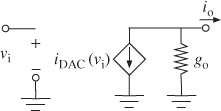
B.5 
where ![]() and
and ![]() represent the modulator FS reference current and voltage, respectively.
represent the modulator FS reference current and voltage, respectively.
The model parameters included in the Ideal_DAC_for_SI model are the following:
- Gain, that models the DAC gain; that is,
 .
. - Gout, that represents
 .
. - Sampling Time, that models the clock period.
- Input Clock Phase; that is, the clock phase at which the DAC input is sampled.
Ideal_DAC_dig_level_SD2
This block transforms a thermometric-coded digital input into its corresponding analog level. The model parameters used in this behavioral model are:
- Vhigh, that defines the upper limit of the quantization FS range.
- Vlow, that corresponds to the lower limit of the quantization FS range.
- Number of levels of the embedded quantizer.
B.3 Real SC Building-Block Libraries
SIMSIDES includes two libraries of SC integrators and two libraries of SC resonators. These libraries are described subsequently.
B.3.1 Real SC Integrators
There are two SC integrator model libraries in SIMSIDES: one including FE SC integrator models and the other one including LD SC integrators. In both cases, integrator models are classified according to the nonideal effects that are included in the model and the number of SC branches connected at the integrator input. This way, for each model there are four building blocks using the same behavioral model except for the number of input SC branches.
As an illustration, Figure B.5 shows the symbol used in SIMSIDES for one-branch SC FE integrators (Figure B.5a) and two-branch SC FE integrators (Figure B.5b), together with their equivalent SC circuits. Note that although single-ended conceptual schematics are shown in this figure, fully-differential circuits are assumed in the behavioral models.
Figure B.5 SC integrator symbol in SIMSIDES: (a) one-branch integrator and (b) two-branch integrator.

Both integrators in Figure B.5 use the same behavioral model that consists of an ideal SC FE integrator with output swing limitation. The behavioral model corresponding to a one-branch SC FE integrator is named Basic_SC_FE_Int, while the model of the two-branch SC FE integrator is named Basic_SC_FE_IntII. Following this nomenclature, Basic_SC_FE_IntIII and Basic_SC_FE_IntIV models are used for three- and four-branch SC FE integrators, respectively.
Table B.2 lists all SC integrator models available in SIMSIDES including a brief description of the nonidealities included in each of them. Note that the model names included in Table B.2 correspond to one-branch integrators. The same models are available for integrators with up to four input branches.
Table B.2 Library of SC (FE/LD) integrators included in SIMSIDES
| Model name | Circuit effects included |
| Basic_SC_FE_Int | Output swing limitation |
| Basic_SC_LD_Int | |
| SC_FE_Int_Non_linear_C | Output swing limitation, |
| SC_LD_Int_Non_linear_C | capacitor nonlinearity. |
| SC_FE_Int_Weight_Mismatch | Output swing limitation, |
| SC_LD_Int_Weight_Mismatch | capacitor mismatch. |
| SC_FE_Int_Non_Linear_Sampling | Output swing limitation, |
| SC_LD_Int_Non_Linear_Sampling | nonlinear switch on-resistance. |
| SC_FE_Int_FiniteDCgain | Finite OTA DC gain, |
| SC_LD_Int_FiniteDCgain | output swing limitation, |
| parasitic OTA caps. | |
| SC_FE_Int_Finite&Non_LinearDCGain | Finite nonlinear OTA DC gain, |
| SC_LD_Int_Finite&Non_LinearDCGain | output swing limitation |
| parasitic OTA caps. | |
| SC_FE_Int_Noise | OTA thermal noise, output swing |
| SC_LD_Int_Noise | limitation, parasitic/load OTA caps. |
| SC_FE_Int_Settling | Incomplete settling error, output swing |
| SC_LD_Int_Settling | limitation, parasitic/load OTA caps. |
| SC_FE_Integrator_All_Effects | switch on-resistance, |
| SC_LD_Integrator_All_Effects | capacitor nonlinearity and mismatch, |
| settling error, finite (nonlinear) DC gain, | |
| thermal noise, parasitic/load capacitors, | |
| output swing limitation. | |
| SC_FE_Integrator_All_Effects&NonLinSamp | switch nonlinear on-resistance, |
| SC_LD_Integrator_All_Effects&NonLinSamp | capacitor nonlinearity and mismatch, |
| settling error, finite (nonlinear) DC gain, | |
| thermal noise, parasitic/load capacitors, | |
| output swing limitation. | |
| SC_FE_Int_1b_SD2 | switch on-resistance and its effect on |
| GB and SR, | |
| capacitor nonlinearity and mismatch, | |
| settling error, finite (nonlinear) DC gain, | |
| thermal noise, parasitic/load capacitors, | |
| output swing limitation. | |
| SC_FE_Int_1b_DEM_SD2 | switch on-resistance and its effect on |
| GB and SR, | |
| array of unit sampling capacitors, | |
| capacitor nonlinearity and mismatch, | |
| settling error, finite (nonlinear) DC gain, | |
| thermal noise, parasitic/load capacitors, | |
| output swing limitation. |
The model named SC_FE_Int_1b_SD2 represents one-branch SC FE integrators with all circuit nonideal effects, including the degradation caused by the switch on-resistance on the integrator GB and SR. In this model, notation 1b is used for denoting one input SC branch. Similarly, other models the names of which include nb denote n input SC branches.
The model named SC_FE_Int_1b_DEM_SD2 includes the same nonideal effects as SC_FE_Int_1b_SD2 model but it also allows modeling the sampling capacitor as an array of unit capacitors. This array is used in combination with multilevel quantizers and DACs that incorporate DWA/DEM algorithms as described in Section B.8. In this way, the number of unit capacitors in the array must be exactly the same as the number of DAC levels. Moreover, this array should include the DAC mismatch error that can be modeled as a Gaussian distribution. Both SC_FE_Int_1b_SD2 and SC_FE_Int_1b_DEM_SD2 models provide detailed information about the integrator equivalent input-referred thermal noise, equivalent load capacitances, and transient response model parameters. All these pieces of information are displayed in the MATLAB command window after simulation.
Table B.3 lists the most important parameters used by the SC integrator behavioral models in SIMSIDES, as well as a brief description of all of them.
Table B.3 Model parameters used in SIMSIDES SC (FE/LD) integrators
| Parameter name (in alphabetical order) | Brief description |
| Array of sampling capacitors | Array of unit capacitors |
| for DEM branch | used with multilevel DACs with DEM |
| B (switch parameters) | MOS large-signal transconductance |
| (analytic model) | |
| Bandwidth (BW) | Input signal bandwidth |
| Capacitor (first/second)-order | Capacitor (first/second) |
| nonlinearity | order nonlinearity |
| Finite and Linear Ron | switch on-resistance, linear model |
| Finite DC Gain of the AO | Finite OTA DC gain |
| g (switch parameters) | Finite switch on-conductance |
| (analytic model) | |
| Identifier for this integrator | Identifier used for settling error model |
| Input Equivalent Thermal Noise | OTA input-referred thermal noise |
| Input parameters [A,fi,ph] (switch) | Amplitude, frequency, and phase of |
| the sinewave input | |
| (table look-up model) | |
| Integration/Sampling Capacitor | Integration/sampling capacitors |
| Integration additional load | Additional load capacitance |
| at the integration phase | |
| Load Capacitor (cload) | Integrator load capacitance |
| Maximum output current (Io) | OTA maximum output current |
| Nonlinearity of the DC Gain | OTA DC gain nonlinear coefficients |
| Output Swing Up/Down | Maximum/minimum output swing limits |
| Parasitic Capacitor before the AO (Cp) | Parasitic capacitance at the OTA input |
| pcoef (switch parameters) | nonlinear coefficients of |
| the switch on-resistance | |
| (table look-up model) | |
| Positive Input is Sampled in... | Input-switch clock phase |
| Ron | switch on-resistance |
| Sampling additional load | Additional load capacitance |
| at the sampling phase | |
| Sampling Time | Clock signal period |
| Switch on-resistance (Ron) | Switch on-resistance |
| Temp | Temperature (K) |
| Transconductance of the AO (gm) | OTA transconductance |
| Variance | Variance of the capacitor mismatch error |
B.3.2 Real SC Resonators
SIMSIDES has two SC resonator model libraries corresponding to FEI-based resonators and LDI-based resonators. All building-block models correspond to the ![]() -domain block diagrams shown in Figure B.1 but they are implemented by using the SC integrator models described in the previous section. As an illustration, Figure B.6 shows the SIMSIDES block diagram of an SC LDI-based resonator (Figure B.6a) and an SC FEI-based resonator (Figure B.6b), which correspond to Figures B.1a and B.1b, respectively.
-domain block diagrams shown in Figure B.1 but they are implemented by using the SC integrator models described in the previous section. As an illustration, Figure B.6 shows the SIMSIDES block diagram of an SC LDI-based resonator (Figure B.6a) and an SC FEI-based resonator (Figure B.6b), which correspond to Figures B.1a and B.1b, respectively.
Figure B.6 Block diagram of SC resonators in SIMSIDES: (a) LDI-based resonator and (b) FEI-based resonator.

Following the same philosophy as that used in SC integrators, the behavioral models of SC resonators in SIMSIDES are classified attending to the number of input SC branches and the circuit nonideal effects included in the models. As an illustration, Figure B.7 shows an excerpt of both SC resonators libraries. Note that each row of blocks includes the same circuit nonideal effects, with the only difference among them being the number of input branches.
Figure B.7 Excerpt of SC resonator libraries in SIMSIDES.

Table B.4 lists all SC resonator models available in SIMSIDES, including a brief description of the nonidealities considered in each of them. The parameters used in these models are the same as those included in SC integrator models—listed in Table B.3. In addition to these parameters, the resonator gain can also be defined by the user by setting a parameter named Gain (see Figure B.6), that can be defined in the model dialogue box.
Table B.4 Library of SC (FE/LD) resonators included in SIMSIDES
| Model name | Circuit effects included |
| Basic_SC_FE_Res | Output swing limitation |
| Basic_SC_LD_Res | |
| SC_FE_Res_NonLinear_C | Output swing limitation, |
| SC_LD_Res_NonLinear_C | capacitor nonlinearity. |
| SC_FE_Res_Weight_Mismatch | Output swing limitation, |
| SC_LD_Res_Weight_Mismatch | capacitor mismatch. |
| SC_FE_Res_Non_Linear_Sampling | Output swing limitation, |
| SC_LD_Res_Non_Linear_Sampling | nonlinear switch on-resistance. |
| SC_FE_Res_FiniteDCgain | Finite OTA DC gain, |
| SC_LD_Res_FiniteDCgain | output swing limitation, |
| parasitic OTA caps. | |
| SC_FE_Res_FiniteDC&NonLinearGain | Finite nonlinear OTA DC gain, |
| SC_LD_Res_FiniteDC&NonLinearGain | output swing limitation, |
| parasitic OTA caps. | |
| SC_FE_Res_Noise | OTA thermal noise, output swing |
| SC_LD_Res_Noise | limitation, parasitic/load OTA caps. |
| SC_FE_Res_Settling | Incomplete settling error, output swing |
| SC_LD_Res_Settling | limitation, parasitic/load OTA caps. |
| SC_FE_Res_All_effects | switch on-resistance, |
| SC_LD_Res_All_effects | capacitor nonlinearity and mismatch, |
| settling error, finite (nonlinear) DC gain, | |
| thermal noise, parasitic/load capacitors. | |
| SC_FE_Res_All_effects&NonLinSamp | switch nonlinear on-resistance, |
| SC_LD_Res_All_effects&NonLinSamp | capacitor nonlinearity and mismatch, |
| settling error, finite (nonlinear) DC gain, | |
| thermal noise, parasitic/load capacitors, | |
| output swing limitation. |
B.4 Real SI Building-Block Libraries
SIMSIDES includes all necessary building blocks for the simulation of SI-![]() Ms. This section describes SI integrators and resonators, as well as their main model parameters.
Ms. This section describes SI integrators and resonators, as well as their main model parameters.
B.4.1 Real SI Integrators
Following the same classification criteria as that followed for SC building-block models, there are two libraries of SI integrators in SIMSIDES: one including FE SI integrators and the other one including LD SI integrators. Figure B.8 shows the symbol used in SIMSIDES for SI integrators together with a conceptual schematic of an FE SI integrator and an LD SI integrator. In both cases, different models are included in SIMSIDES, which are classified attending to the number of nonideal effects that are taken into account, as detailed in Table B.5.
Figure B.8 SI integrator symbol used in SIMSIDES and its corresponding conceptual schematics.

Table B.5 Library of SI (FE/LD) integrators included in SIMSIDES
| Model name | Circuit effects included |
| Ideal_SI_FE_Integrator | Ideal SI (FE/LD) integrator. |
| Ideal_SI_LD_Integrator | |
| Basic_SI_FE_Integrator | Output current limits, |
| Basic_SI_LD_Integrator | nonlinear gain. |
| SI_FE_Int_Finite_Conductance | Output current limits, |
| SI_LDI_Finite_Conductance | finite nonlinear |
| output conductance, | |
| input voltage limits, | |
| thermal noise. | |
| SI_FE_Int_Finite_Conductance&Settling | Output current limits, |
| SI_LDI_Finite_Conductance&Settling | finite nonlinear |
| input/output conductance, | |
| input voltage limits, | |
| settling error, | |
| thermal noise. | |
| SI_FE_Int_Finite_...&Settling&Charge_Injection | Output current limits, |
| SI_LDI_Finite_...&Settling&Charge_Injection | finite nonlinear |
| input/output conductance, | |
| input voltage limits, | |
| settling error, thermal noise, | |
| charge injection error. |
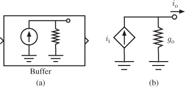
Apart from the building blocks in Table B.5, a current-mode buffer block, named Buffer, is included in all SIMSIDES SI libraries. This block transforms an input current vector into an output matrix made up of two vector elements: the input current signal itself in parallel with an output conductance, named Gout of the source in the model. Figure B.9 illustrates the operation of the Buffer block, by showing the SIMSIDES block symbol and its equivalent circuit.
Figure B.9 SI buffer used in SIMSIDES: (a) symbol and (b) equivalent circuit.
B.4.2 Real SI Resonators
As in the case of SC circuits, two different types of SI resonators are modeled in SIMSIDES, namely SI FEI-based resonators and LDI-based resonators. Both block diagrams are depicted in Figure B.10. In both cases, integrator gain parameters—denoted as Affe, Afb1, and Afa2—can be defined by the user in the block dialogue window, as well as their associated gain errors—respectively denoted in the model as MU1, MU2, MU3.
Figure B.10 Block diagram of SI resonators in SIMSIDES: (a) FEI-loop resonator and (b) LDI-loop resonator.

Table B.6 lists all SI resonator blocks included in SIMSIDES together with a brief description of the error mechanisms taken into account in each model. These errors and their associated model parameters, which are the same as those used in SI integrators, are described here.
Table B.6 Library of SI (FE/LD) resonators included in SIMSIDES
| Model name | Circuit effects included |
| Ideal_SI_FE_Resonator | Ideal SI (FE/LD) resonator. |
| Ideal_SI_LD_Resonator | |
| Basic_SI_FE_Resonator | Output current limits, |
| Basic_SI_LD_Resonator | nonlinear gain. |
| SI_FE_Res_Finite_Conductance | Output current limits, |
| SI_LD_Resonator_Finite_Conductance | finite nonlinear |
| output conductance, | |
| input voltage limits, | |
| thermal noise. | |
| SI_FE_Res_Finite_Conductance&Settling | Output current limits, |
| SI_LD_Res_Finite_Conductance&Settling | finite nonlinear |
| input/output conductance, | |
| input voltage limits, | |
| settling error, | |
| thermal noise. | |
| SI_FE_Res_Finite_...&Settling&Charge_Injection | Output current limits, |
| SI_LD_Res_Finite_...&Settling&Charge_Injection | finite nonlinear |
| input/output conductance, | |
| input voltage limits, | |
| settling error, thermal noise, | |
| charge injection error. |
B.4.3 SI Errors and Model Parameters
This section gives a brief description of the main errors and model parameters included in SI model libraries of SIMSIDES. For the sake of clarity, these errors are linked to some of the building blocks in which they are included.
Basic_SI_FE(LD)_Integrator and Basic_SI_FE(LD)_Resonator
The model parameters included in these blocks are:
- Integrator Gain: integrator weight (see Figure B.8).
- Iomax(=-Iomin): maximum/minimum integrator output current.
- MU1,MU3: first-order and third-order coefficients of the gain nonlinearity.
The ![]() -domain transfer function of this integrator block is given by the following expression,
-domain transfer function of this integrator block is given by the following expression,
B.6 ![]()
where ![]() is the
is the ![]() -transform of the ideal output current.
-transform of the ideal output current.
The abovementioned expression is also used for both LDI- and FEI-based SI resonators, although in this case the nonlinear coefficients are named SHI1, SHI3 instead of MU1, MU3.
SI_FE(LD)_Int_Finite_Conductance
These blocks include the effect of finite input–output conductance ratio error. To this purpose, the equivalent circuit shown in Figure B.11 is solved during sampling phase. This circuit corresponds to the SI LD integratorB.1 of Figure B.8 on clock phase ![]() . In this circuit, the input signal is modeled as an ideal current in parallel with a finite conductance, denoted as
. In this circuit, the input signal is modeled as an ideal current in parallel with a finite conductance, denoted as ![]() . Memory-cell transistor 1 (M1) is configured in the hold phase and is modeled by its drain current
. Memory-cell transistor 1 (M1) is configured in the hold phase and is modeled by its drain current ![]() in parallel with an output conductance
in parallel with an output conductance ![]() . In contrast, memory-cell transistor 2 (M2) is operating in sampling phase and it is modeled by the parallel connection of its output conductance with an input resistor. This resistor is a nonlinear function of the drain current
. In contrast, memory-cell transistor 2 (M2) is operating in sampling phase and it is modeled by the parallel connection of its output conductance with an input resistor. This resistor is a nonlinear function of the drain current ![]() of M2, given by,
of M2, given by,
Figure B.11 Modeling finite input–output conductance ratio error in SIMSIDES: (a) SI LD integrator and (b) equivalent circuit during sampling phase (![]() ).
).

where A1, A3 represent the first-order and third-order nonlinear coefficients of the input resistance. These parameters are defined in the models together with the following ones:
- Gout: output conductance
 of memory cells.
 - Vmax/Vmin: maximum/minimum values of
 in Equation B.7.
 - Ibias: integrator bias current (see Figure B.8).
SI_FE(LD)_Int_Finite_Conductance&Settling&ChargeInjection
Those SI building blocks including nonlinear incomplete settling and charge injection require the following additional model parameters:
- Gmo: operating-point small-signal transconductance of memory transistors.
- Cgs: gate-to-source capacitance of memory transistors.
- Eq: charge injection error.
The charge injection error Eq is defined as a relative error on the voltage stored in the gate-to-source capacitance, given by:
B.8 ![]()
B.5 Real CT Building-Block Libraries
Figure B.12 shows the CT building-block model libraries included in SIMSIDES. There are four libraries of CT integrators and two libraries of CT resonators, which are classified attending to the circuit nature of the building blocks, namely Gm-C, Gm-MC, Gm-LC, active-RC, and MOSFET-C.
Figure B.12 Classification of SIMSIDES CT model libraries.

B.5.1 Real CT Integrators
Tables B.10 list all modelsB.2 included in CT integrator libraries shown in Figure B.12, together with a brief description of the nonideal effects included. An explanation of the most representative blocks and their associated model parameters is given in the following sections.
Model Parameters Used in Transconductors and Gm-C Integrator Building Blocks
Building blocks listed in Table B.7 are used in SIMSIDES to model transconductors and Gm-C integrators, considering the effect of different circuit-level nonideal effects. This section gives a description of the most significant model parameters included in these blocks.
Table B.7 Gm-C integrator library models in SIMSIDES
| Model name | Circuit effects included |
| Ideal_OTA_C_CTint | Ideal Gm-C integrator. |
| Transconductor | Input saturation voltage, |
| nonlinear transconductance. | |
| gm_no_noise_new | Output saturation voltage, |
| third-order intercept point. | |
| 1pole_gm | Gm-C output impedance. |
| OTA_C_CT_1pole | Input/output saturation voltage, |
| finite OTA DC gain, nonlinear transconductance, | |
| one-pole dynamic, time-constant error, | |
| nonlinear transconductance, thermal noise. | |
| OTA_C_CT_2poles | Input/output saturation voltage, |
| OTA_C_CT_2polesb | Finite OTA DC gain, nonlinear transconductance, |
| two-pole dynamic, time-constant error, | |
| nonlinear transconductance, thermal noise. |
Table B.8 Gm-MC integrator library models in SIMSIDES
| Model name | Circuit effects included |
| Gm_MC_CTInt_1pole | Input/output saturation voltage, |
| finite OTA DC gain, parasitic capacitances, | |
| one-pole dynamic, thermal noise. | |
| Gm_MC_CTInt_2poles | Input/output saturation voltage, |
| finite OTA DC gain, parasitic capacitances, | |
| two-pole dynamic, thermal noise. | |
| Gm...1pole&Large_signal_distortion | Input/output saturation voltage, |
| output current limit, finite OTA DC gain, | |
| parasitic capacitances, one-pole dynamic. | |
| Gm...2poles&Large_signal_distortion | Input/output saturation voltage, |
| output current limit, finite OTA DC gain, | |
| parasitic capacitances, two-pole dynamic. | |
| Gm...1pole&Small_Signal_Distortion | Input/output saturation voltage, |
| output current limit, finite OTA DC gain, | |
| nonlinear transconductance, | |
| parasitic capacitances, one-pole dynamic. | |
| Gm...2poles&Small_Signal_Distortion | Input/output saturation voltage, |
| output current limit, finite OTA DC gain, | |
| nonlinear transconductance, | |
| parasitic capacitances, two-pole dynamic. |
Table B.9 Active-RC integrator library models in SIMSIDES
| Model name | Circuit effects included |
| RC_CTInt_1pole | OTA output swing limitation, |
| finite OTA DC gain, parasitic capacitances, | |
| capacitance voltage coefficient, | |
| one-pole dynamic, thermal noise. | |
| RC_CTInt_2poles | OTA output swing limitation, |
| finite OTA DC gain, parasitic capacitances, | |
| capacitance voltage coefficient, | |
| two-pole dynamic, thermal noise. | |
| RC...1pole&Large_signal_distortion | OTA output swing limitation, |
| output current limit, finite OTA DC gain, | |
| parasitic capacitances, | |
| capacitance voltage coefficient, | |
| one-pole dynamic, thermal noise. | |
| RC...2poles&Large_signal_distortion | OTA output swing limitation, |
| output current limit, finite OTA DC gain, | |
| parasitic capacitances, | |
| capacitance voltage coefficient, | |
| two-pole dynamic, thermal noise. | |
| RC_Int_1in | OTA output swing limitation, |
| RC_Int_2in | finite OTA DC gain, nonlinear trans., |
| RC_Int_3in | slew rate, parasitic capacitances, |
| one-pole dynamic, thermal noise. |
Table B.10 MOSFET-C integrator library models in SIMSIDES
| Model name | Circuit effects included |
| MOSFET_C_CTInt_1pole | OTA output swing limitation, |
| finite OTA DC gain, parasitic capacitances, | |
| capacitance voltage coefficient, | |
| one-pole dynamic, thermal noise. | |
| MOSFET_C_CTInt_2poles | OTA output swing limitation, |
| finite OTA DC gain, parasitic capacitances, | |
| capacitance voltage coefficient, | |
| two-pole dynamic, thermal noise. | |
| MOS...1pole&Large_signal_distortion | OTA output swing limitation, |
| output current limit, finite OTA DC gain, | |
| parasitic capacitances | |
| one-pole dynamic, thermal noise. | |
| MOS...2poles&Large_signal_distortion | OTA output swing limitation, |
| output current limit, finite OTA DC gain, | |
| parasitic capacitances | |
| two-pole dynamic, thermal noise. |
Transconductance of the OTA and Integration Capacitor, define, respectively, the transconductance ![]() and the integration capacitor
and the integration capacitor ![]() of the Gm-C integrator, the ITF of which is obtained by replacing
of the Gm-C integrator, the ITF of which is obtained by replacing ![]() in Equation B.1.
in Equation B.1.
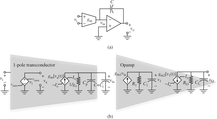
[Upper,Lower] bound saturation voltage defines the maximum and minimum values of the output voltage ![]() , as illustrated in Figure B.13.
, as illustrated in Figure B.13.
Figure B.13 One-pole Gm-C integrator model used in SIMSIDES.

Input Voltage [Upper, Lower] saturation limit defines the maximum and minimum values of the input voltage, denoted as ![]() and
and ![]() , respectively, in Figure B.13.
, respectively, in Figure B.13.
[Second, Third] order distortion coefficient represents the second- and third-order nonlinear transconductance coefficients ![]() , where it is assumed that the transconductance depends on the Gm-C integrator input voltage
, where it is assumed that the transconductance depends on the Gm-C integrator input voltage ![]() as,
as,
with ![]() being the nominal value of the transconductance. The maximum current provided by the transconductor is defined as
being the nominal value of the transconductance. The maximum current provided by the transconductor is defined as ![]() .
.
DC voltage gain represents the finite OTA DC gain, defined as ![]() , with
, with ![]() being the output conductance of the Gm-C integrator.
being the output conductance of the Gm-C integrator.
Integration constant time error, defined as ![]() , with
, with ![]() being the parasitic capacitance at the output of the Gm-C integrator.
being the parasitic capacitance at the output of the Gm-C integrator.
High-frequency pole that defines the value of the high-frequency pole when a two-pole dynamic model is considered.
Gm-MC Integrators
SIMSIDES contains a library of Gm-C integrators based on the connection of a transconductance element and a Miller capacitance, also referred to as Gm-MC integrators. Figure B.14a shows the conceptual schematic of the Gm-MC integrators modeled in SIMSIDES. Several models that account for the effect of different circuit nonidealities are included in this library. The most accurate one, named Gm_MC_CTInt_1poleSmall_Signal_Distortion, is modeled by the equivalent circuit shown in Figure B.14b that involves a two-pole dynamic model. In addition to the model parameters included in Gm-C integrators, Gm-MC integrator models use the additional parameters described below.
Figure B.14 Two-pole Gm-MC integrator model used in SIMSIDES: (a) conceptual schematic and (b) equivalent circuit of the transconductor and the opamp.
Output transconductor parasitic, Integration capacitor ratio (Cp/C) that represents ![]() (see Figure B.14b).
(see Figure B.14b).
Output Operational parasitic, Integration capacitor ratio (CI/C); that is, ![]() .
.
Operational parasitic Output, OTA output capacitor ratio (Ct/C); that is, ![]() .
.
Transconductor and Op. Amplifier Unity gain frequency (Hz) [Gb1, Ga2], that represent the GB of the transconductor and of the opamp in Figure B.14b, respectively.
High-frequency pole, that defines the value of the high-frequency (nondominant) pole when a two-pole dynamic is considered—given by ![]() in Figure B.14b.
in Figure B.14b.
Origin transconductance, that refers to the operating-point transconductance ![]() of the nonlinear characteristic given in Equation B.9.
of the nonlinear characteristic given in Equation B.9.
Active-RC Integrators
Among all active-RC integrator models listed in Table B.9, the most accurate and complete one is named RC_CTInt_2poles&Large_signal_distortio. Figure B.15 shows the conceptual schematic (Figure B.15a) and its corresponding equivalent model (Figure B.15b). There are two versions of this model: one based on a linear input resistance ![]() and another in which
and another in which ![]() is a nonlinear function of the input voltage given by,
is a nonlinear function of the input voltage given by,
Figure B.15 Two-pole active-RC integrator model used in SIMSIDES: (a) conceptual schematic and (b) equivalent circuit.

B.10 ![]()
where ![]() represents the first- and second-order nonlinear coefficients.
represents the first- and second-order nonlinear coefficients.
Apart from the model parameters used by the CT building blocks described in previous sections, the following parameters are used in active-RC integrator models:
Output resistance—integration resistance ratio, that represents ![]() in Figure B.15b.
in Figure B.15b.
Integrator Ideal Unity gain frequency (RC), defined as ![]() .
.
Opamp ideal Unity gain frequency, that is the GB of the opamp in Figure B.15b.
High-frequency pole (Hz), defined as ![]() (see Figure B.15b).
(see Figure B.15b).
MOSFET-C Integrators
In addition to active-RC integrator models, SIMSIDES includes also a library of MOSFET-C integrators the conceptual schematic of which is shown in Figure B.16. Essentially, these building blocks are the same as those used for modeling active-RC integrators, except that the integrator resistance ![]() is replaced by a MOSFET transistor.
is replaced by a MOSFET transistor.
Figure B.16 Conceptual schematic of a MOSFET-C integrator similar to that modeled in SIMSIDES by the building blocks listed in Table B.10.

B.5.2 Real CT Resonators
Tables B.11 and B.12 list all models included in CT resonator libraries shown in Figure B.12, together with a brief description of their nonideal effects. These libraries include different building blocks that are classified according to the accuracy of their models as well as to the circuit nonidealities that are taken into account. As an illustration, Figure B.17 depicts both CT resonator libraries included in SIMSIDES, namely Gm-C resonators and Gm-LC resonators. Figure B.18 shows the conceptual schematic of both kinds of CT resonators. The model parameters involved in the building blocks shown in Figure B.17 are detailed here.
Table B.11 Gm-C resonator library models in SIMSIDES
| Model name | Circuit effects included |
| Ideal_gmC_CT_Resonator | Ideal Gm-C resonator. |
| gmC_CT_Res_1pole | Finite OTA DC gain, |
| time-constant error, | |
| one-pole dynamic, thermal noise. | |
| gmC_CT_Res_2poles | Finite OTA DC gain, |
| gmC_CT_Res_2polesfull | time-constant error, |
| two-pole dynamic, thermal noise. | |
| gmC_CT_Res_1pole_larged | Input/output saturation voltage, |
| output current limit, finite OTA DC gain, | |
| time-constant error, one-pole dynamic. | |
| gmC_CT_Res_2poles_larged | Input/output saturation voltage, |
| output current limit, finite OTA DC gain, | |
| nonlinear transconductance, | |
| time-constant error, two-pole dynamic. | |
| gmC_CT_Res_1pole_small&larged | Input/output saturation voltage, |
| output current limit, finite OTA DC gain, | |
| nonlinear transconductance, | |
| time-constant error, one-pole dynamic. | |
| gmC_CT_Res_2poles_small&larged | Input/output saturation voltage, |
| output current limit, finite OTA DC gain, | |
| nonlinear transconductance, | |
| time-constant error, two-pole dynamic. |
Table B.12 Gm-LC resonator library models in SIMSIDES
| Model name | Circuit effects included |
| Ideal_gmLC_CT_Resonator | Ideal Gm-LC resonator. |
| gmLC_CT_Res_1pole | Input/output saturation voltage, |
| inductance quality factor and series parasitic resistance, | |
| finite OTA DC gain, time-constant error, | |
| one-pole dynamic, thermal noise. | |
| gmLC_CT_Res_2poles | Input/output saturation voltage, |
| inductance quality factor and series parasitic resistance, | |
| finite OTA DC gain, time-constant error, | |
| two-pole dynamic, thermal noise. | |
| gmLC...1pole_large_dist | Input/output saturation voltage, |
| inductance quality factor and series parasitic resistance, | |
| output current limitation, | |
| finite OTA DC gain, time-constant error, | |
| one-pole dynamic, thermal noise. | |
| gmLC...2poles_large_dist | Input/output saturation voltage, |
| inductance quality factor and series parasitic resistance, | |
| output current limitation, | |
| finite OTA DC gain, time-constant error, | |
| two-pole dynamic, thermal noise. | |
| gm...1pole_small&large_dist | Input/output saturation voltage, |
| inductance quality factor and series parasitic resistance, | |
| output current limitation, nonlinear transconductance, | |
| finite OTA DC gain, time-constant error, | |
| one-pole dynamic, thermal noise. | |
| gmLC...2poles_small&larged | Input/output saturation voltage, |
| inductance quality factor and series parasitic resistance, | |
| output current limitation, nonlinear transconductance, | |
| finite OTA DC gain, time-constant error, | |
| two-pole dynamic, thermal noise. |
Figure B.17 CT resonator libraries included in SIMSIDES: (a) Gm-C resonators and (b) Gm-LC resonators.

Figure B.18 Conceptual schematics of the CT resonators modeled in SIMSIDES: (a) Gm-C resonator and (b) Gm-LC resonator.

Gm-C Resonators
Apart from those parameters used in Gm-C integrators, the following model parameters are used in the Gm-C resonator model library:
Transconductance of the first, second, and third OTA (gm1,gm2,gm3); that is, ![]() , and
, and ![]() in Figure B.18a.
in Figure B.18a.
Capacitors; that is, ![]() in Figure B.18a.
in Figure B.18a.
Nonlinear transconductance coefficients [gmnl1, gmnl2], that represents nonlinear coefficients ![]() in Equation B.9.
in Equation B.9.
DC Gain of OTAs [Av1,Av2,Av3], that defines the finite OTA DC gain of transconductors in Figure B.18a.
Percentual integration constant time error [et1, et2]; that is, the time constant errors associated with both feed-forward transconductances in Figure B.18a, given by,
B.11 ![]()
where ![]() represents the parasitic capacitance of the
represents the parasitic capacitance of the ![]() th transconductance in Figure B.18a.
th transconductance in Figure B.18a.
Gm-LC Resonators
The main model parameters used by Gm-LC resonator blocks are described in this section. Essentially, these parameters deal with the inductor element in Figure B.18b and its associated resonant frequency.
Frequency resonance; that is, the resonant frequency of the Gm-LC resonator.
Inductor Q; that is, the Q-factor of the inductor in Figure B.18b.
Series Resistance; that is, the parasitic resistance ![]() of the inductor.
of the inductor.
The rest of the model parameters used in Gm-C resonators have the same meaning as those used in Gm-C integrators and resonators.
B.6 Real Quantizers and Comparators
Table B.13 lists the building blocks included in the real Quantizers&Comparators SIMSIDES library, together with a brief description of their operation and main circuit nonidealities. In addition to the ideal parameters described in Section B.2.3, additional model parameters are required to model the different circuit nonidealities. These error parameters are listed in Table B.14.
Table B.13 Real Quantizers and Comparator models included in SIMSIDES
| Model name | Circuit effects included |
| Real_Comparator_Offset&Hysteresis | Voltage-mode comparator |
| with offset, | |
| (random & deterministic) hysteresis. | |
| Real_Comparator_Offset&Hysteresis_for_SI | Current-mode comparator |
| with offset | |
| and nonlinearity (INL). | |
| Real_Multibit_Quantizer | Voltage-mode multibit quantizer |
| with gain error, offset | |
| (random & deterministic) hysteresis. | |
| Real_Multibit_Quantizer_for_SI | Current-mode multibit quantizer |
| with gain error, offset, INL, | |
| (random & deterministic) hysteresis. | |
| Real_Multibit_Quantizer_dig_level_SD2 | Voltage-mode multilevel quantizer |
| with gain error, offset, INL, | |
| (random & deterministic) hysteresis. | |
| Real_Sampler | Sampling & Hold circuit with |
| clock jitter error. |
Table B.14 Error model parameters used in SIMSIDES Real Quantizers
| Parameter name (in alphabetical order) | Brief description |
| Gain Error in LSB | Gain error measured in LSB. |
| Jitter typical deviation | Standard deviation of clock jitter error. |
| Kind of Hysteresis | Comparator hysteresis. It may |
| be either deterministic or random hysteresis. | |
| INL in LSB | Integral Nonlinearity error measured in LSB. |
| Number of levels | Number of quantizer levels. |
| Offset | Offset error. |
| Offset Error in LSB | Offset error measured in LSB. |
| Seed for random jitter generation | Seed number used for |
| generating random jitter error. |
Note that apart from comparators and quantizers, there is a building block named Real_Sampler that is used for modeling the S&H circuits that are connected at the input of embedded quantizers in CT-![]() Ms. One of the most critical errors associated with this building block is the clock jitter. It is modeled as an uncertainty in the sampling time
Ms. One of the most critical errors associated with this building block is the clock jitter. It is modeled as an uncertainty in the sampling time ![]() corresponding to a stationary process with zero mean and standard deviation defined by the user (see Table B.14).
corresponding to a stationary process with zero mean and standard deviation defined by the user (see Table B.14).
B.7 Real D/A Converters
Table B.15 lists the different building blocks included in the real D/A Converters SIMSIDES library, together with a brief description of their operation and main circuit errors.
Table B.15 Real DAC models included in SIMSIDES
| Model name | Circuit effects included |
| Real_DAC_Multibit | Voltage-mode multibit DAC |
| with offset, gain error, and INL error. | |
| Real_DAC_Multibit_SI | Current-mode multibit DAC |
| with offset, gain error, and INL error. | |
| Real_DAC_Multibit_delay_Jitter | Voltage-mode multibit DAC |
| with offset error, | |
| gain error, INL error, | |
| delay error, and clock jitter error. | |
| Real_DAC_Multibit_delay_Jitter_SI | Current-mode multibit DAC |
| with finite output conductance, offset error, | |
| gain error, INL error, | |
| delay error, and clock jitter error. | |
| Real_DAC_pulse_types | Voltage-mode multibit DAC |
| with selectable NRZ/RZ/HRZ output waveform. | |
| Real_DAC_Multibit_pulse_types | Voltage-mode multibit DAC |
| with selectable NRZ/RZ/HRZ output waveform, | |
| gain error, offset error, and INL error. | |
| Real_DAC..._delay_jitter | Voltage-mode multibit DAC |
| with selectable NRZ/RZ/HRZ output waveform, | |
| gain error, offset error, INL error, | |
| delay error, and clock jitter error. |
Error parameters associated with the models listed in Table B.15 have the same meaning as those used in multibit quantizers, except for the selectable NRZ/RZ/HRZ DAC waveform and the delay error. The latter can be chosen to be either a constant delay or a signal-dependent delay, given by,
B.12 ![]()
where d0, d1, x1, dmax are model parameters set by the user.
B.8 Auxiliary Blocks
In addition to the building blocks described in previous sections, SIMSIDES includes a library named Auxiliary blocks that contains some other blocks (such as adders, DEM algorithms, and digital latches) also needed to simulate ![]() Ms. Table B.16 lists the models included in the mentioned library together with a brief description of their operation. The most significant parameters used by these models are listed in Table B.17.
Ms. Table B.16 lists the models included in the mentioned library together with a brief description of their operation. The most significant parameters used by these models are listed in Table B.17.
Table B.16 Auxiliary building-block models used in SIMSIDES
| ANALOG ADDERS | |
| Model name | Brief description |
| Analog_Adder_Ideal_SD2 | Ideal SC passive adder with |
| parasitic input capacitance and load capacitance. | |
| Analog_Adder_real_SD2 | Real SC passive adder with |
| parasitic input capacitance and load capacitance, | |
| switch on-resistance, settling error, | |
| capacitor nonlinearity, and thermal noise. | |
| DIGITAL ADDERS | |
| Model name | Brief description |
| Dig_add_generic_2outs | Digital subtraction of a |
| Dig_add_3L_5L_13L | signal and a |
| Dig_add_3L_3L_5L_2outs | which is scaled by a factor of d. The result is a |
| Dig_add_3L_3L_7L_2outs | |
| Dig_add_3L_5L_9L_2outs | |
| Dig_add_3L_5L_13L_2outs | |
| DIGITAL LATCHES | |
| Model name | Brief description |
| D_latch_simplest | Digital “D” latches. |
| D_latch | |
| DAC WITH DEM ALGORITHMS | |
| Model name | Brief description |
| DEM_id_SD2 | Ideal DEM algorithm. |
| DAC - DEM - V04 | DAC block with a selectable DEM algorithm. |
| There are three options: No DEM, DWA, Pseudo-DWA. | |
| Mux_SD2 | Building block used for sampling an input (analog) signal |
| by a number of different branches corresponding | |
| to the number of DAC unit capacitors. | |
Table B.17 Error model parameters used in SIMSIDES Auxiliary Blocks
| Parameter name (in alphabetical order) | Brief description |
| Comparator Input Capacitor (C) | Parasitic capacitance at the |
| comparator/quantizer input. | |
| DEM type | DEM algorithm: (1) No DEM, |
| (2) DWA, (3) Pseudo-DWA. | |
| (Default = 1) | |
| Input Capacitor (C) | Input capacitance of the analog adder. |
| Nonlinearities of the capacitors | Capacitance nonlinear coefficients |
| in an analog adder. | |
| Number of elements | Number of DAC unit elements. |
| Output type | Digital output code: (1) Binary output, |
| (2) Trilevel output including common | |
| mode (Default = 1). | |
| Time interval between sampling | Delay between the time instant when |
| and comparison (delta) | the adding operation is performed |
| and the time instant when | |
| comparison time takes place. |
As an illustration on the use of some of the auxiliary blocks, Figure B.19a shows the SIMSIDES block diagram of a second-order feed-forward SC-![]() M, which includes an embedded 16-level quantizer and DAC with a selectable DEM algorithm.
M, which includes an embedded 16-level quantizer and DAC with a selectable DEM algorithm.
Figure B.19 Example of a second-order feed-forward SC-![]() M with 16-level quantization and DEM: (a) SIMSIDES block diagram, (b) Mux_SD2 dialogue box, (c) first integrator block dialogue box, (d) second integrator block dialogue box, and (e) DAC-DEM block dialogue box.
M with 16-level quantization and DEM: (a) SIMSIDES block diagram, (b) Mux_SD2 dialogue box, (c) first integrator block dialogue box, (d) second integrator block dialogue box, and (e) DAC-DEM block dialogue box.

The block diagram in Figure B.19a includes the following building blocks:
- Mux_SD2. This block samples the modulator input signal in a number of unit capacitors, which corresponds to the number of unit elements used in the multilevel DAC minus one. As shown in Figure B.19b, the only model parameter of this block is named Number of elements, which equals 15 in this example.
- SC_FE_Int_All_Effects_DEM_SD2. This block is used for modeling the front-end integrator and includes all error mechanisms with values defined in the block dialogue box in Figure B.19c. This model includes also a parameter named Array of sampling capacitors for DEM branch. The number of capacitors in the array must be exactly the same as the number of DAC levels, that is, the number of quantization levels. As an illustration, Figure B.20 shows the MATLAB code used for generating different alternative capacitor arrays together with other parameters used for simulating the block diagram in Figure B.19a. Note that this capacitor array must include also the DAC element mismatch, defined as a Gaussian probability distribution.
Figure B.20 MATLAB code used for defining capacitor arrays and DEM parameters of Figure B.19e.

- Basic_SC_FE_Int. This block is used for modeling the second integrator, considering only ideal values of the output swing and capacitors, as shown in Figure B.19d.
- Real_Multibit_Quantizer_dig_level_SD2. This block, named Q1 in the example, is used for modeling the quantizer considering the nonideal effects listed in Table B.13. In this example, these nonideal effects have not been taken into account. The output of this block is a thermometric-coded bit array. This array is transformed into an analog signal for further processing by using the block named ThermometricCode-to-Analog.
- DAC-DEM. This block uses the DAC - DEM - V04 model (see Table B.16). The most important model parameters of these block are highlighted in Figure B.19e.
As an illustration, Figure B.21 shows the output spectra of the ![]() M in Figure B.19a considering a capacitor mismatch of
M in Figure B.19a considering a capacitor mismatch of ![]() . It is clear how the performance of the modulator becomes severely degraded by DAC nonlinearity if DEM is not activated (DEM type 1).
. It is clear how the performance of the modulator becomes severely degraded by DAC nonlinearity if DEM is not activated (DEM type 1).
Figure B.21 Effect of DEM on the output spectrum of the ![]() M of Figure B.19a.
M of Figure B.19a.

B.1 A similar circuit is used for SI FE integrators.
B.2 RC_Int_1,2,3in models allow setting up of transistor-level parameters such as channel-length modulation, gate-to-source overdrive voltage, saturation voltage, supply voltage, etc.