
Chapter 5
Frontiers of ΣΔ Modulators: Trends and Challenges
Since the introduction of the ![]() modulation technique, there has been a pleiad of ICs published; implemented using many diverse technology processes, architectural, and circuit techniques, which have targeted a huge number of applications that span from sensors and instrumentation to ultra-low power, biomedical applications, and broadband communications [1–3].
modulation technique, there has been a pleiad of ICs published; implemented using many diverse technology processes, architectural, and circuit techniques, which have targeted a huge number of applications that span from sensors and instrumentation to ultra-low power, biomedical applications, and broadband communications [1–3].
An in-depth understanding of the performance of state-of-the-art ![]() Ms, their trends, challenges, and circuits and systems solutions, constitutes a powerful and empirical tool for designers to select the optimum
Ms, their trends, challenges, and circuits and systems solutions, constitutes a powerful and empirical tool for designers to select the optimum ![]() M architecture, circuit implementation, technology process, etc, for a given set of specifications and/or a particular application. With this objective in mind and following the practical approach considered throughout this book, this chapter gives an overview of reported cutting-edge
M architecture, circuit implementation, technology process, etc, for a given set of specifications and/or a particular application. With this objective in mind and following the practical approach considered throughout this book, this chapter gives an overview of reported cutting-edge ![]() M ICs fabricated in CMOS technologies. The main purpose of this overview is to make an exhaustive analysis of the evolution trends, design challenges, and reported solutions in order to extract practical conclusions and guidelines which may be useful for designers in their own projects.
M ICs fabricated in CMOS technologies. The main purpose of this overview is to make an exhaustive analysis of the evolution trends, design challenges, and reported solutions in order to extract practical conclusions and guidelines which may be useful for designers in their own projects.
The study described here is inspired by previous surveys on state-of-the-art performance of ADCs [3–10]. In the majority of cases, these surveys cover different kinds of ADCs, not only ![]() Ms. Among others, the surveys published by Walden [4], Murmann [5], and more recently Jonsson [8, 9] and Manganaro [10], are particularly exhaustive and accurate. Compared to these works, the study described in this book focuses on
Ms. Among others, the surveys published by Walden [4], Murmann [5], and more recently Jonsson [8, 9] and Manganaro [10], are particularly exhaustive and accurate. Compared to these works, the study described in this book focuses on ![]() M ICs; emphasizing on the different architectures and circuits used in many different applications. Moreover, in addition to analyzing statistics and comparing data collected from publications and extracted from standard performance metrics, the study presented in this chapter gives an overview of cutting-edge
M ICs; emphasizing on the different architectures and circuits used in many different applications. Moreover, in addition to analyzing statistics and comparing data collected from publications and extracted from standard performance metrics, the study presented in this chapter gives an overview of cutting-edge ![]() M circuits and systems techniques which are at the frontier of state-of-the-art performance, highlighting the incoming trends and challenges as well as the proposed efficient solutions.
M circuits and systems techniques which are at the frontier of state-of-the-art performance, highlighting the incoming trends and challenges as well as the proposed efficient solutions.
The data used for this study was mainly collected from the IEEE Journal of Solid-State Circuits as well as the major conferences sponsored by the IEEE Solid-State Circuits Society (SSCS), namely International Solid-State Circuits Conference (ISSCC), European Solid-State Circuits Conference (ESSCIRC), Custom Integrated Circuits Conference (CICC), Symposium on VLSI Circuits (VLSI), Asian Solid-State Circuits Conference (ASSCC), and Radio Frequency Integrated Circuits Symposium (RFIC). In addition to these SSCS publications, some other remarkable ![]() M ICs published in the IEEE Transactions on Circuits and Systems (parts I and II) and the IEEE International Symposium on Circuits and Systems (ISCAS) have also been collected in the survey.Overall, more than 300
M ICs published in the IEEE Transactions on Circuits and Systems (parts I and II) and the IEEE International Symposium on Circuits and Systems (ISCAS) have also been collected in the survey.Overall, more than 300 ![]() M ICs have been analyzed in detail and considered in this review. Although the works under study include papers published since 1990 to June 2012, data was more exhaustively collected in the last 10 years.
M ICs have been analyzed in detail and considered in this review. Although the works under study include papers published since 1990 to June 2012, data was more exhaustively collected in the last 10 years.
All data collected and analyzed in the survey is compiled in an Excel spreadsheet that is available online at http://www.imse-cnm.csic.es/∼jrosa/CMOS-SDMs-Survey-IMSE-JMdelaRosa.xlsx. The database in this spreadsheet file is periodically kept up to date every six months and aims to be a complement to the popular and highly cited Murmann's ADC survey data collection [11].
Following this introduction, the chapter is organized as follows. Section 5.1 gives an overview of the state-of-the-art ![]() Ms, comparing their performance with Nyquist-rate ADCs. The diverse families of
Ms, comparing their performance with Nyquist-rate ADCs. The diverse families of ![]() M architectures and circuit techniques are exhaustively analyzed and compared in Section 5.2 in order to extract practical and empirical design guidelines. Section 5.3 reviews some of the most significant cutting-edge
M architectures and circuit techniques are exhaustively analyzed and compared in Section 5.2 in order to extract practical and empirical design guidelines. Section 5.3 reviews some of the most significant cutting-edge ![]() M techniques, analyzing the design trends and challenges in the frontiers of
M techniques, analyzing the design trends and challenges in the frontiers of ![]() Ms. Finally, the chapter is concluded with a classified description of state-of-the-art references.
Ms. Finally, the chapter is concluded with a classified description of state-of-the-art references.
5.1 Overview of the State of the Art on  Ms
Ms
Tables 5.13 sum up the performance of the state-of-the-art ![]() M ICs considered in this survey. For the sake of clarity and simplicity, the ICs included in the study have been classified according to their architecture/circuit characteristics into the following tables:
M ICs considered in this survey. For the sake of clarity and simplicity, the ICs included in the study have been classified according to their architecture/circuit characteristics into the following tables:
- SC-
 Ms: single-loop single-bit LP-
 Ms (Table 5.1), single-loop multibit LP-
 Ms (Table 5.2), cascade single-bit LP-
 Ms (Table 5.3), cascade multibit LP-
 Ms (Table 5.4), and BP-
 Ms (Table 5.5).
 - CT-
 Ms: single-loop single-bit LP-
 Ms (Table 5.6), single-loop multibit LP-
 Ms (Table 5.7), cascade LP-
 Ms (Table 5.8), and BP-
 Ms (Table 5.9).
  Ms with time-coded quantization (Table 5.10).
- Hybrid
 Ms: CT/DT
  Ms, active/passive
  Ms, digital-based
  Ms, and
  M/Nyquist-rate ADCs (Table 5.11).
 - Reconfigurable
 Ms implemented using SC (Table 5.12) and CT circuits (Table 5.13).
Table 5.1 State-of-the-art SC single-loop single-bit LP-![]() Ms
Ms

The ![]() M ICs are sorted by FOM. Engineering notation is used for
M ICs are sorted by FOM. Engineering notation is used for ![]() and power consumption.
and power consumption.
Table 5.2 State-of-the-art SC single-loop multibit LP-![]() Ms
Ms

The ![]() M ICs are sorted by FOM. Architecture is expressed in terms of the modulator order and the number of bits/levels of the embedded quantizer. For instance, 2nd-ord(4b) represents a second-order loop filter with 4-bit quantizer and 5th-ord(33L) means a fifth-order architecture with 33-level quantizer.
M ICs are sorted by FOM. Architecture is expressed in terms of the modulator order and the number of bits/levels of the embedded quantizer. For instance, 2nd-ord(4b) represents a second-order loop filter with 4-bit quantizer and 5th-ord(33L) means a fifth-order architecture with 33-level quantizer.
Table 5.3 State-of-the-art SC cascade single-bit LP-![]() Ms
Ms
The cascade topology is expressed in terms of the stage orders. For instance, notation 2-2 is used for representing a fourth-order cascade ![]() M made up of two second-order stages.
M made up of two second-order stages.
Table 5.4 State-of-the-art SC cascade multibit LP-![]() Ms
Ms

The number of bits per levels of the quantizer is given in parentheses. This way, notation 2-1(5L) is used for denoting a cascade 2-1 ![]() M topology with 5-level quantizer in the second stage. If no parentheses are shown, single-bit quantization is assumed in a given modulator stage.
M topology with 5-level quantizer in the second stage. If no parentheses are shown, single-bit quantization is assumed in a given modulator stage.
Table 5.5 State-of-the-art SC BP-![]() Ms
Ms

Table 5.6 State-of-the-art CT single-loop single-bit LP-![]() Ms
Ms
Table 5.7 State-of-the-art CT single-loop multibit LP-![]() Ms
Ms

Table 5.8 State-of-the-art CT cascade LP-![]() Ms
Ms

I/Q is used for denoting a quadrature topology.
Table 5.9 State-of-the-art CT BP-![]() Ms
Ms

Table 5.10 State-of-the-art ![]() Ms with time-coded quantization
Ms with time-coded quantization
TDC stands for time-to-digital converter; TEQ stands for time-encoding quantizer.
Table 5.11 State-of-the-art hybrid ![]() Ms
Ms

Table 5.12 State-of-the-art SC adaptive/reconfigurable ![]() Ms
Ms
For the sake of clarity, and considering that reconfigurable ![]() Ms feature different performance depending on their operating mode, the ICs in this table have been sorted by the year of publication.
Ms feature different performance depending on their operating mode, the ICs in this table have been sorted by the year of publication.
Table 5.13 State-of-the-art CT adaptive/reconfigurable ![]() Ms
Ms
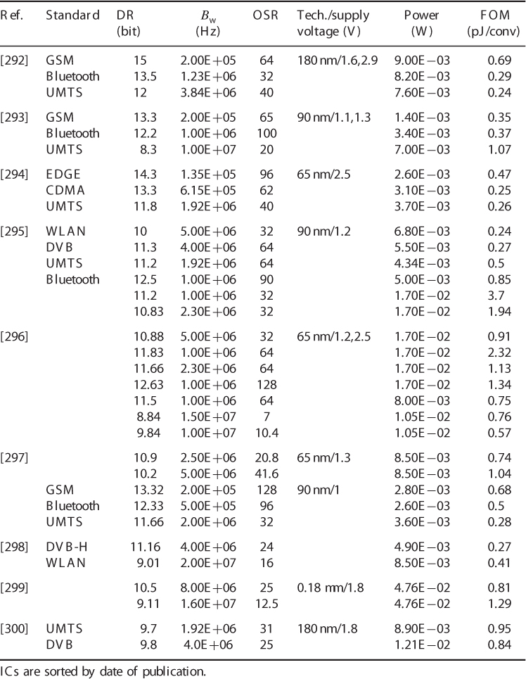
ICs are sorted by date of publication.
In all cases, the main features of each reported IC are summarized in terms of the following performance metrics: DR (measured in bits), ![]() , OSR, technology process, supply voltage, and power consumption.1 In the case of BP-
, OSR, technology process, supply voltage, and power consumption.1 In the case of BP-![]() Ms (Tables 5.5 and 5.9), the notch frequency
Ms (Tables 5.5 and 5.9), the notch frequency ![]() is also given. A schematic description of each
is also given. A schematic description of each ![]() M topology is sketched in the tables, highlighting the loop-filter order, the number of stages (in cascade
M topology is sketched in the tables, highlighting the loop-filter order, the number of stages (in cascade ![]() Ms), the number of bits of the embedded quantizer, the type of quantization technique (in time-based quantizers), the operation mode and standard covered (in the case of reconfigurable
Ms), the number of bits of the embedded quantizer, the type of quantization technique (in time-based quantizers), the operation mode and standard covered (in the case of reconfigurable ![]() Ms), etc. A more complete description of the modulators—not shown in the tables of this chapter for the sake of simplicity–can be found in the spreadsheet available on the Web.
Ms), etc. A more complete description of the modulators—not shown in the tables of this chapter for the sake of simplicity–can be found in the spreadsheet available on the Web.
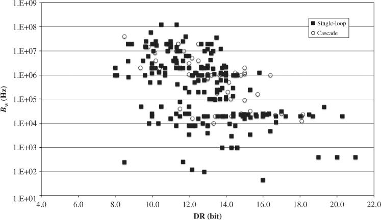
5.1.1 DR-versus- Conversion Region
Figure 5.1 represents DR versus ![]() for the different families of
for the different families of ![]() Ms.2 It can be noted in Figure 5.1 that a wide DR-versus-
Ms.2 It can be noted in Figure 5.1 that a wide DR-versus-![]() conversion region is covered, ranging over seven decades in frequency and 16 bit in the DR axis. The highest DR is 21 bit, which was reported in 1994 by Kerth et al. who designed a fourth-order single-loop single-bit SC-
conversion region is covered, ranging over seven decades in frequency and 16 bit in the DR axis. The highest DR is 21 bit, which was reported in 1994 by Kerth et al. who designed a fourth-order single-loop single-bit SC-![]() M in a 3-µm CMOS technology which digitized 400-Hz signals for seismic applications [48]. On the other hand, the highest value of
M in a 3-µm CMOS technology which digitized 400-Hz signals for seismic applications [48]. On the other hand, the highest value of ![]() was reported by Shibata et al. at ISSCC in February 2012. This chip consisted of a DC-to-1-GHz tunable notch-frequency sixth-order multibit LP/BP CT-
was reported by Shibata et al. at ISSCC in February 2012. This chip consisted of a DC-to-1-GHz tunable notch-frequency sixth-order multibit LP/BP CT-![]() M, implemented in a 65-nm CMOS technology, achieving 12-bit DR within a 150 MHz signal bandwidth [239].
M, implemented in a 65-nm CMOS technology, achieving 12-bit DR within a 150 MHz signal bandwidth [239].
Figure 5.1 DR-versus-![]() conversion region of state-of-the-art CMOS
conversion region of state-of-the-art CMOS ![]() Ms.
Ms.

Figure 5.2 compares the conversion region achieved by the state-of-the-art ![]() Ms with the one achieved by Nyquist-rate CMOS ADCs. The data in this figure was collected from Murmann's ADC survey [11], as well as from that used in Figure 5.1. It can be observed from Figure 5.2 that
Ms with the one achieved by Nyquist-rate CMOS ADCs. The data in this figure was collected from Murmann's ADC survey [11], as well as from that used in Figure 5.1. It can be observed from Figure 5.2 that ![]() ADCs dominate the state-of-the-art DR-versus-
ADCs dominate the state-of-the-art DR-versus-![]() front in a wide frequency range: from hundreds of hertz to hundreds of megahertz. Beyond this range, Nyquist-rate are more competitive, reporting state-of-the-art performance in high-frequency applications with signal bandwidths ranging from hundreds of megahertz to dozens of gigahertz.
front in a wide frequency range: from hundreds of hertz to hundreds of megahertz. Beyond this range, Nyquist-rate are more competitive, reporting state-of-the-art performance in high-frequency applications with signal bandwidths ranging from hundreds of megahertz to dozens of gigahertz.
Figure 5.2 Comparison of the DR-versus-![]() conversion region of
conversion region of ![]() M and Nyquist-rate ADCs. In all cases, only CMOS ICs are considered.
M and Nyquist-rate ADCs. In all cases, only CMOS ICs are considered.

Analyzing the evolution over time of the ![]() handled by
handled by ![]() Ms, it can be observed that the tendency is toward extending their range of application, particularly increasing the digitized signal bandwidth, although these designs—placed in the so-called technology front—are sometimes less power efficient, as will be discussed later. Figure 5.3 represents the
Ms, it can be observed that the tendency is toward extending their range of application, particularly increasing the digitized signal bandwidth, although these designs—placed in the so-called technology front—are sometimes less power efficient, as will be discussed later. Figure 5.3 represents the ![]() reported by
reported by ![]() Ms over time of publication for the years 1990–2012. It can be observed how
Ms over time of publication for the years 1990–2012. It can be observed how ![]() Ms have evolved from low-frequency (high-resolution) to high-frequency (medium-to-low resolution) applications. Note also that the range of
Ms have evolved from low-frequency (high-resolution) to high-frequency (medium-to-low resolution) applications. Note also that the range of ![]() is spread over time from two orders of magnitude to over six orders of magnitude. This trend benefits from the technology downscaling and it is expected to continue in the coming years.
is spread over time from two orders of magnitude to over six orders of magnitude. This trend benefits from the technology downscaling and it is expected to continue in the coming years.
Figure 5.3 ![]() spread of
spread of ![]() Ms over time for the years 1990–2012.
Ms over time for the years 1990–2012.

5.1.2 Conversion Energy and Figures of Merit
Apart from their main specifications (DR (or SNDR) and ![]() ), the efficiency of ADCs is quantified in terms of the power consumption required to achieve these specifications. Taking all these ingredients into account, the amount of energy per converted sample
), the efficiency of ADCs is quantified in terms of the power consumption required to achieve these specifications. Taking all these ingredients into account, the amount of energy per converted sample ![]() —also referred to as conversion energy [5]—can be calculated as [5, 9],
—also referred to as conversion energy [5]—can be calculated as [5, 9],
5.1 ![]()
where ![]() is the power consumption and
is the power consumption and ![]() represents the digital output rate of the ADC, that is, the Nyquist rate, measured in samples per second (S/s).
represents the digital output rate of the ADC, that is, the Nyquist rate, measured in samples per second (S/s).
Thus, it is common to analyze and graphically represent the efficiency of ADCs in the form of plots of conversion energy versus DR or SNDR—also known as energy plots [5, 10]. As an illustration, Figure 5.4 shows the energy plot of state-of-the-art ![]() Ms. Note that, in order to compute the overall performance achieved by a given
Ms. Note that, in order to compute the overall performance achieved by a given ![]() M, both magnitudes involved in Figure 5.4—that is, the conversion energy
M, both magnitudes involved in Figure 5.4—that is, the conversion energy ![]() and the resolution (expressed in terms of either DR or SNDR)—must be taken into account. As expected, there is a direct relationship between DR and
and the resolution (expressed in terms of either DR or SNDR)—must be taken into account. As expected, there is a direct relationship between DR and ![]() , so that the larger the resolution, the more conversion energy is needed.
, so that the larger the resolution, the more conversion energy is needed.
Figure 5.4 Energy plot of state-of-the-art ![]() Ms.
Ms.

It is therefore convenient to express the trade-off highlighted in Figure 5.4 between the conversion energy and DR in a single performance metric to quantify the performance of a given ![]() M and to compare the performance of different ADC architectures. Such a performance metric is often referred to as figure of merit (
M and to compare the performance of different ADC architectures. Such a performance metric is often referred to as figure of merit (![]() ), and accounts in a single formula the three basic specifications of an ADC, namely effective resolution, signal bandwidth, and power consumption.
), and accounts in a single formula the three basic specifications of an ADC, namely effective resolution, signal bandwidth, and power consumption.
Choosing the appropriate ![]() is always a matter of debate and discussion. Among others, the following expressions that relate
is always a matter of debate and discussion. Among others, the following expressions that relate ![]() with ENOB have been most frequently used for comparing the performance of ADCs [4, 102, 301]
with ENOB have been most frequently used for comparing the performance of ADCs [4, 102, 301]
5.2 ![]()
5.3 ![]()
where ![]() is the Boltzmann constant and
is the Boltzmann constant and ![]() is the chip temperature (measured in Kelvin).
is the chip temperature (measured in Kelvin).
Note that ![]() emphasizes power consumption, whereas
emphasizes power consumption, whereas ![]() emphasizes effective resolution. Therefore, the smaller the
emphasizes effective resolution. Therefore, the smaller the ![]() value and the larger the
value and the larger the ![]() value, the “better” the ADC is. In this chapter,
value, the “better” the ADC is. In this chapter, ![]() has been selected because it has been the most commonly used FOM in the recent years by the majority of the
has been selected because it has been the most commonly used FOM in the recent years by the majority of the ![]() M community. It should be noted that according to the definition of ENOB given in Equation 1.20, DR was used for computing ENOB and consequently for the value of
M community. It should be noted that according to the definition of ENOB given in Equation 1.20, DR was used for computing ENOB and consequently for the value of ![]() as shown in Tables 5.13. However, in those
as shown in Tables 5.13. However, in those ![]() M ICs presenting a strongly nonlinear behavior, the effective resolution (i.e., ENOB) is indeed limited by the peak SNDR, as stated in Chapter 1 and hence, its corresponding
M ICs presenting a strongly nonlinear behavior, the effective resolution (i.e., ENOB) is indeed limited by the peak SNDR, as stated in Chapter 1 and hence, its corresponding ![]() is worse than the one shown in the tables. However, the purpose of this chapter is to analyze the overall performance and trends of
is worse than the one shown in the tables. However, the purpose of this chapter is to analyze the overall performance and trends of ![]() ADCs, instead of the specifications achieved by a particular design. From this perspective, and considering that not all authors reported all data required to compute
ADCs, instead of the specifications achieved by a particular design. From this perspective, and considering that not all authors reported all data required to compute ![]() , the analysis was based on expressions of
, the analysis was based on expressions of ![]() derived from DR, instead of from SNDR.
derived from DR, instead of from SNDR.
Thus, following an approach similar to that proposed by Murmann [5], the results reported by state-of-the-art performance ![]() Ms are compared in Figure 5.4 with two straight lines for the numerical examples of
Ms are compared in Figure 5.4 with two straight lines for the numerical examples of ![]() 100 fJ/conversion-step and 10 fJ/conversion-step. Note that the majority of
100 fJ/conversion-step and 10 fJ/conversion-step. Note that the majority of ![]() Ms reaching the lowest values of
Ms reaching the lowest values of ![]() are placed between both lines and correspond to CT circuit implementations, showing the best efficiency of these kinds of
are placed between both lines and correspond to CT circuit implementations, showing the best efficiency of these kinds of ![]() Ms for resolutions in the order of 11–15-bit DR within 1–100 MHz bandwidths, as will be discussed later in this chapter.
Ms for resolutions in the order of 11–15-bit DR within 1–100 MHz bandwidths, as will be discussed later in this chapter.
Figure 5.5 represents ![]() versus
versus ![]() for the different
for the different ![]() M architectures included in Tables 5.13. It can be seen how CT-
M architectures included in Tables 5.13. It can be seen how CT-![]() Ms obtain better performance than SC-
Ms obtain better performance than SC-![]() Ms for
Ms for ![]() MHz, while SC-
MHz, while SC-![]() Ms are more efficient for lower values of
Ms are more efficient for lower values of ![]() . In terms of architectures, it can be noted how LP-
. In terms of architectures, it can be noted how LP-![]() Ms obtain better values of
Ms obtain better values of ![]() than BP-
than BP-![]() Ms. This is due to the fact that CT BP-
Ms. This is due to the fact that CT BP-![]() Ms digitize signals placed at a notch frequency
Ms digitize signals placed at a notch frequency ![]() , which in the majority of cases is in the order of hundreds of megahertz and even in the gigahertz range (Table 5.9). However, this parameter is not considered in
, which in the majority of cases is in the order of hundreds of megahertz and even in the gigahertz range (Table 5.9). However, this parameter is not considered in ![]() , which penalizes its performance compared to LP-
, which penalizes its performance compared to LP-![]() Ms as will be discussed later.
Ms as will be discussed later.
Figure 5.5 ![]() versus
versus ![]() corresponding to the state-of-the-art
corresponding to the state-of-the-art ![]() Ms under study.
Ms under study.

Figure 5.6 compares the value of ![]() achieved by state-of-the-art
achieved by state-of-the-art ![]() Ms with that achieved by Nyquist-rate ADCs. Note that
Ms with that achieved by Nyquist-rate ADCs. Note that ![]() Ms show a competitive performance in a wide range of
Ms show a competitive performance in a wide range of ![]() , from hundreds of hertz to hundreds of megahertz. Only SAR ADCs achieve lower values of
, from hundreds of hertz to hundreds of megahertz. Only SAR ADCs achieve lower values of ![]() within the interval 10 kHz
within the interval 10 kHz ![]() 10 MHz. Pipeline ADCs are the best choice for those applications with 100 MHz
10 MHz. Pipeline ADCs are the best choice for those applications with 100 MHz ![]() 1 GHz, whereas flash ADCs dominate for
1 GHz, whereas flash ADCs dominate for ![]() 1 GHz.
1 GHz.
Figure 5.6 Comparison of ![]() ADCs and Nyquist-rate ADCs in terms of
ADCs and Nyquist-rate ADCs in terms of ![]() versus
versus ![]() .
.

In terms of conversion energy, (as illustrated in Figure 5.7), ![]() ADCs are more efficient than SAR and pipeline ADCs for applications requiring DR
ADCs are more efficient than SAR and pipeline ADCs for applications requiring DR ![]() 12 bit, while SAR ADCs require the lowest conversion energy within the 8–12-bit resolution interval.
12 bit, while SAR ADCs require the lowest conversion energy within the 8–12-bit resolution interval.
Figure 5.7 Comparison of energy plot of state-of-the-art ![]() Ms, SAR, and pipeline ADCs.
Ms, SAR, and pipeline ADCs.

5.2 Empirical and Statistical Analysis of State-of-the-Art  Ms
Ms
Analyzing in detail the data included in Tables 5.13, a number of interesting conclusions can be drawn. This section aims to identify practical pieces of information that can be used as guidelines for designers to make a better decision on the best architecture and circuit technique for a given set of specifications.
5.2.1 SC versus CT State-of-the-Art  Ms
Ms
Although SC circuit technique has been traditionally used in most reported ![]() Ms, more and more ICs are being implemented using CT circuits, especially in those applications targeting broadband signals and/or requiring low power consumption. Overall, approximately 57
Ms, more and more ICs are being implemented using CT circuits, especially in those applications targeting broadband signals and/or requiring low power consumption. Overall, approximately 57![]() of
of ![]() M ICs included in this survey are implemented using SC circuits, whereas 43
M ICs included in this survey are implemented using SC circuits, whereas 43![]() of them are CT-
of them are CT-![]() Ms. However, as illustrated in Figure 5.8, there is a tendency, in recent years, to use CT techniques. This trend is expected to continue as this kind of
Ms. However, as illustrated in Figure 5.8, there is a tendency, in recent years, to use CT techniques. This trend is expected to continue as this kind of ![]() Ms will benefit from the technology downscaling process and the increase in transition frequency. Indeed, the decrease in voltage supplies (and consequently the voltage headroom) together with the increasing use of digital signal processing and calibration techniques are favoring the implementation of CT-
Ms will benefit from the technology downscaling process and the increase in transition frequency. Indeed, the decrease in voltage supplies (and consequently the voltage headroom) together with the increasing use of digital signal processing and calibration techniques are favoring the implementation of CT-![]() Ms in nanometer CMOS processes, increasing their operating frequency more and more [10].
Ms in nanometer CMOS processes, increasing their operating frequency more and more [10].
Figure 5.8 Number of SC- and CT-![]() Ms published for the years 1990–2012.
Ms published for the years 1990–2012.

Figure 5.9a represents the aperture plot [5] (i.e., ![]() vs DR) corresponding to the state-of-the-art SC- and CT-
vs DR) corresponding to the state-of-the-art SC- and CT-![]() Ms. Note that two state-of-the-art fronts (highlighted in the figure) can be clearly identified. One front—dominated by CT-
Ms. Note that two state-of-the-art fronts (highlighted in the figure) can be clearly identified. One front—dominated by CT-![]() Ms—goes from approximately 10-bit to 14-bit DR, covering a
Ms—goes from approximately 10-bit to 14-bit DR, covering a ![]() range from 10 to 150 MHz. The other front—covered by SC-
range from 10 to 150 MHz. The other front—covered by SC-![]() Ms—goes from 14-bit to 21-bit DR with
Ms—goes from 14-bit to 21-bit DR with ![]() ranging from 400 Hz to 2 MHz. Therefore, as could be logically expected, it can be empirically deduced from these results that CT-
ranging from 400 Hz to 2 MHz. Therefore, as could be logically expected, it can be empirically deduced from these results that CT-![]() Ms are more suitable for medium-resolution (10–14 bit) and medium–high bandwidths (10–100 MHz), whereas SC-
Ms are more suitable for medium-resolution (10–14 bit) and medium–high bandwidths (10–100 MHz), whereas SC-![]() Ms are more appropriate for applications requiring high-resolutions (15–20 bit) within low-medium bandwidths (100 Hz–1 MHz).
Ms are more appropriate for applications requiring high-resolutions (15–20 bit) within low-medium bandwidths (100 Hz–1 MHz).
Figure 5.9 Comparison between state-of-the-art SC- and CT-![]() Ms: (a) aperture plot (
Ms: (a) aperture plot (![]() versus DR) and (b) energy plot (
versus DR) and (b) energy plot (![]() versus
versus ![]() ).
).

The resolution-versus-bandwidth regions covered by the state-of-the-art fronts drawn in Figure 5.9a define the application areas where SC- and CT-![]() Ms are more efficient. This is illustrated in Figure 5.9b, where the energy plot is compared for both circuit techniques. Overall, it can be concluded that CT-
Ms are more efficient. This is illustrated in Figure 5.9b, where the energy plot is compared for both circuit techniques. Overall, it can be concluded that CT-![]() Ms are more efficient than SC-
Ms are more efficient than SC-![]() Ms for
Ms for ![]() .
.
5.2.2 Gm-C versus Active-RC State-of-the-Art CT- Ms
Ms
As already discussed in this book, CT-![]() Ms can be implemented using either active-RC or Gm-C integrators. Active-RC integrators have the advantages of better linearity and larger signal swing, whereas Gm-C integrators are potentially faster with less power consumption, at the price of reducing their linearity as compared to active-RC integrators [302]. In practice, the majority of state-of-the-art CT-
Ms can be implemented using either active-RC or Gm-C integrators. Active-RC integrators have the advantages of better linearity and larger signal swing, whereas Gm-C integrators are potentially faster with less power consumption, at the price of reducing their linearity as compared to active-RC integrators [302]. In practice, the majority of state-of-the-art CT-![]() Ms have been implemented using active-RC integrators. Sometimes an active-RC front-end integrator is chosen for its better linearity, whereas the rest integrators of the
Ms have been implemented using active-RC integrators. Sometimes an active-RC front-end integrator is chosen for its better linearity, whereas the rest integrators of the ![]() M loop-filter are of Gm-C type. This is the most common situation in LP-
M loop-filter are of Gm-C type. This is the most common situation in LP-![]() Ms, while most BP-
Ms, while most BP-![]() Ms operating at notch frequencies in the order of hundreds of megahertz or in the gigahertz band, have been implemented using either Gm-C or Gm-LC integrators.
Ms operating at notch frequencies in the order of hundreds of megahertz or in the gigahertz band, have been implemented using either Gm-C or Gm-LC integrators.
Figure 5.10a illustrates the conversion region covered by the different CT circuit techniques by showing the aperture plot of state-of-the-art CT-![]() Ms. For the sake of clarity, the different families of CT-
Ms. For the sake of clarity, the different families of CT-![]() Ms have been organized into three categories: Gm-C, active-RC, and active-RC/Gm-C. The latter assumes that only the front-end integrator is active-RC while the remaining ones in the modulator chain are implemented using Gm-C techniques. It can be noted that the state-of-the-art front (highlighted in the figure) is dominated by active-RC implementations.
Ms have been organized into three categories: Gm-C, active-RC, and active-RC/Gm-C. The latter assumes that only the front-end integrator is active-RC while the remaining ones in the modulator chain are implemented using Gm-C techniques. It can be noted that the state-of-the-art front (highlighted in the figure) is dominated by active-RC implementations.
Figure 5.10 Gm-C versus active-RC CT-![]() Ms: (a) aperture plot and (b)
Ms: (a) aperture plot and (b) ![]() versus
versus ![]() .
.

In terms of ![]() , active-RC CT-
, active-RC CT-![]() Ms have demonstrated to be more efficient than Gm-C implementations, as illustrated in Figure 5.10b. It can be shown how active-RC
Ms have demonstrated to be more efficient than Gm-C implementations, as illustrated in Figure 5.10b. It can be shown how active-RC ![]() Ms obtain lower values of
Ms obtain lower values of ![]() in a wide range of
in a wide range of ![]() —from 100 kHz to almost 100 MHz.
—from 100 kHz to almost 100 MHz.
5.2.3 Technology Used in State-of-the-Art  Ms
Ms
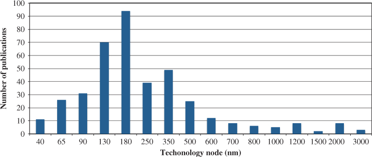
A variety of CMOS processes can be distinguished in Tables 5.13. These technologies have been used in the last 20 years by state-of-the-art ![]() Ms—going from micrometer CMOS (3-µm technology node) down to nanometer processes (40 nm). Supply voltages have scaled down with technology evolution from
Ms—going from micrometer CMOS (3-µm technology node) down to nanometer processes (40 nm). Supply voltages have scaled down with technology evolution from ![]() 6.5 to 0.5 V. As an illustration, Figure 5.11 shows an histogram of the CMOS technologies employed by the
6.5 to 0.5 V. As an illustration, Figure 5.11 shows an histogram of the CMOS technologies employed by the ![]() Ms considered in this survey. Note that 180-nm CMOS process has been the technology node most commonly employed in recent years, mainly using a single 1.8-V supply voltage.
Ms considered in this survey. Note that 180-nm CMOS process has been the technology node most commonly employed in recent years, mainly using a single 1.8-V supply voltage.
Figure 5.11 Histogram of CMOS technologies used by state-of-the-art ![]() Ms.
Ms.
As discussed in Section 5.1.1, ![]() Ms have demonstrated state-of-the-art performance in many diverse processes, taking advantage of the technology downscaling to create the conditions to increase their conversion region. This is illustrated in Figure 5.12, where
Ms have demonstrated state-of-the-art performance in many diverse processes, taking advantage of the technology downscaling to create the conditions to increase their conversion region. This is illustrated in Figure 5.12, where ![]() is represented over the technology node. Note that the minimum value of
is represented over the technology node. Note that the minimum value of ![]() achieved by
achieved by ![]() Ms decreases with the technology downscaling, reaching the lowest values for 180-nm CMOS processes.
Ms decreases with the technology downscaling, reaching the lowest values for 180-nm CMOS processes.
Figure 5.12 ![]() versus CMOS process nodes from
versus CMOS process nodes from ![]() m to 40 nm.
m to 40 nm.

5.2.4 Single-Loop versus Cascade State-of-the-Art  Ms
Ms
Single-loop architectures have been more used than cascade topologies. Overall, approximately 80![]() of the state-of-the-art
of the state-of-the-art ![]() M ICs considered in this survey are single-loop topologies, whereas only 20
M ICs considered in this survey are single-loop topologies, whereas only 20![]() of them are cascades. The latter have been mainly implemented using SC circuits, although recent synthesis methods are making the implementation of CT cascade ICs possible.
of them are cascades. The latter have been mainly implemented using SC circuits, although recent synthesis methods are making the implementation of CT cascade ICs possible.
In terms of the loop-filter order of single-loop architectures, the second-order topology was the most used by SC-![]() Ms, in
Ms, in ![]() of single-bit architectures and
of single-bit architectures and ![]() of multibit topologies (Tables 5.1 and 5.2). In the case of CT implementations, third- and fourth-order topologies were preferred by single-bit topologies, in
of multibit topologies (Tables 5.1 and 5.2). In the case of CT implementations, third- and fourth-order topologies were preferred by single-bit topologies, in ![]() and
and ![]() of cases, respectively (Table 5.6). In the case of multibit implementations, loop-filter orders higher than three were implemented in
of cases, respectively (Table 5.6). In the case of multibit implementations, loop-filter orders higher than three were implemented in ![]() of ICs, taking advantage of the better stability properties of high-order (
of ICs, taking advantage of the better stability properties of high-order (![]() ) implementations with multibit quantization.
) implementations with multibit quantization.
As far as the cascade topologies are concerned (Tables 5.4, and 5.8), the majority of implementations used a fourth-order loop-filter with two stages in a 2-2 configuration or three stages in a 2-1-1 configuration. Third-order 2-1 implementations are also used by SC cascades in ![]() of cases, as shown in Tables 5.3 and 5.4.
of cases, as shown in Tables 5.3 and 5.4.
Figure 5.13 compares the aperture plot of single-loop and cascade state-of-the-art ![]() Ms. It is noted how single-loop dominates almost all ranges of applications from low-bandwidth high-resolution to broadband low-medium resolution. However, as discussed in Section 5.3.1, enhanced techniques are improving the performance of cascade architectures, which may be very suited to implement reconfigurable/adaptive ADCs, thus taking advantage of the very modular nature of the cascade topology.
Ms. It is noted how single-loop dominates almost all ranges of applications from low-bandwidth high-resolution to broadband low-medium resolution. However, as discussed in Section 5.3.1, enhanced techniques are improving the performance of cascade architectures, which may be very suited to implement reconfigurable/adaptive ADCs, thus taking advantage of the very modular nature of the cascade topology.
Figure 5.13 Aperture plot of single-loop and cascade state-of-the-art ![]() Ms. Band-pass, hybrid, and reconfigurable
Ms. Band-pass, hybrid, and reconfigurable ![]() Ms are not included in this plot.
Ms are not included in this plot.
5.2.5 Single-Bit versus Multibit State-of-the-Art  Ms
Ms
Multibit quantization is in general more employed than single-bit quantization. The majority of cascade topologies include dual quantization with a multibit quantizer in the last stage in order to attenuate the impact of the nonlinearity of the feedback DAC. However, increasingly more cascade ICs are including internal quantizers with ![]() ranging from 2 to 5 bit in all stages combined with proper linearization techniques. In addition, a number of
ranging from 2 to 5 bit in all stages combined with proper linearization techniques. In addition, a number of ![]() M ICs are including trilevel quantizers to benefit from the extra level provided by fully differential circuit implementation of the embedded flash ADCs, while keeping an inherent linear behavior of the feedback DAC.
M ICs are including trilevel quantizers to benefit from the extra level provided by fully differential circuit implementation of the embedded flash ADCs, while keeping an inherent linear behavior of the feedback DAC.
In terms of conversion energy, there are more single-bit ![]() Ms than multibit
Ms than multibit ![]() Ms achieving a
Ms achieving a ![]() 100 fJ/conversion-step, as illustrated in the energy plot shown in Figure 5.14a. Although multibit implementations can also achieve a good efficiency for resolutions in the order of 12–16 bit, there are more single-bit solutions reaching state-of-the-art performance within this range.
100 fJ/conversion-step, as illustrated in the energy plot shown in Figure 5.14a. Although multibit implementations can also achieve a good efficiency for resolutions in the order of 12–16 bit, there are more single-bit solutions reaching state-of-the-art performance within this range.
Figure 5.14 Single-bit versus multibit state-of-the-art ![]() Ms: (a) energy plot and (b) aperture plot.
Ms: (a) energy plot and (b) aperture plot.

Figure 5.14b compares the aperture plot of single-bit and multibit ![]() Ms. It is shown how multibit modulators dominate the state-of-the-art fronts except for those applications with resolutions over 20 bit within signal bandwidths below 1 kHz. Indeed, a number of CT-
Ms. It is shown how multibit modulators dominate the state-of-the-art fronts except for those applications with resolutions over 20 bit within signal bandwidths below 1 kHz. Indeed, a number of CT-![]() Ms intended for broadband communications use multibit quantization. Apart from the obvious benefits in terms of the increased number of bits, multibit quantization (and NRZ DAC) is also appealing in practice for its lower sensitivity to clock jitter error, as discussed in Chapter 2. However, the price to pay for using multibit quantization is the inherent nonlinear operation of the multibit feedback DAC, what forces using linearization techniques, with the subsequent penalty in power consumption, speed limitation, and circuit complexity. To address this problem, some authors propose the use of alternative implementations of the modulator feedback waveforms—such as DACs with finite impulsive response (FIR) [154, 161]—to reduce the sensitivity to clock jitter and to relax the
Ms intended for broadband communications use multibit quantization. Apart from the obvious benefits in terms of the increased number of bits, multibit quantization (and NRZ DAC) is also appealing in practice for its lower sensitivity to clock jitter error, as discussed in Chapter 2. However, the price to pay for using multibit quantization is the inherent nonlinear operation of the multibit feedback DAC, what forces using linearization techniques, with the subsequent penalty in power consumption, speed limitation, and circuit complexity. To address this problem, some authors propose the use of alternative implementations of the modulator feedback waveforms—such as DACs with finite impulsive response (FIR) [154, 161]—to reduce the sensitivity to clock jitter and to relax the ![]() M loop-filter linearity specifications, giving rise to a more competitive performance.
M loop-filter linearity specifications, giving rise to a more competitive performance.
5.2.6 Low-Pass versus Band-Pass State-of-the-Art  Ms
Ms
As stated in Section 5.1.2, LP-![]() Ms obtain better performance in terms of
Ms obtain better performance in terms of ![]() than BP-
than BP-![]() Ms. This is better illustrated in Figure 5.15, which compares
Ms. This is better illustrated in Figure 5.15, which compares ![]() of LP- and BP-
of LP- and BP-![]() Ms. Figure 5.16a shows the aperture plot of LP- and BP-
Ms. Figure 5.16a shows the aperture plot of LP- and BP-![]() Ms. Note that the state-of-the-art front is dominated by LP-
Ms. Note that the state-of-the-art front is dominated by LP-![]() Ms, although the highest values of
Ms, although the highest values of ![]() have been reached by BP-
have been reached by BP-![]() Ms.
Ms.
Figure 5.15 Comparison of LP- and BP-![]() Ms:
Ms: ![]() and
and ![]() versus
versus ![]() .
.

Figure 5.16 LP-![]() Ms versus BP-
Ms versus BP-![]() Ms: (a) aperture plot, (b) energy plot, and (c)
Ms: (a) aperture plot, (b) energy plot, and (c) ![]() versus
versus ![]() .
.

Comparing the energy plot of both types of ![]() Ms, it can be shown that LP-
Ms, it can be shown that LP-![]() Ms consume less energy per conversion-step than BP-
Ms consume less energy per conversion-step than BP-![]() Ms, as illustrated in Figure 5.16b, where all
Ms, as illustrated in Figure 5.16b, where all ![]() Ms with
Ms with ![]() 100 fJ/conversion-step are of LP type. However, it should be noted that
100 fJ/conversion-step are of LP type. However, it should be noted that ![]() might not be adequate for quantifying the efficiency of BP-
might not be adequate for quantifying the efficiency of BP-![]() Ms, because
Ms, because ![]() may not always be representative of the operating frequency of the modulator. For instance, looking at Table 5.9, it can be noted that there are several ICs digitizing signals with
may not always be representative of the operating frequency of the modulator. For instance, looking at Table 5.9, it can be noted that there are several ICs digitizing signals with ![]() in the order of 10–20 MHz but placed at center (notch) frequencies in the order of gigahertz. For that reason some authors propose alternative FOMs such as the following one [303]:
in the order of 10–20 MHz but placed at center (notch) frequencies in the order of gigahertz. For that reason some authors propose alternative FOMs such as the following one [303]:
5.4 ![]()
which takes into account not only ![]() , but also the notch frequency
, but also the notch frequency ![]() . As illustrated in Figure 5.15, the use of
. As illustrated in Figure 5.15, the use of ![]() increases the number of state-of-the-art performance BP-
increases the number of state-of-the-art performance BP-![]() Ms, although the comparison may be not fair in this case for LP-
Ms, although the comparison may be not fair in this case for LP-![]() Ms.
Ms.
Figure 5.16c compares the performance of LP- and BP-![]() Ms, based on the following FOM proposed by Schreier and Temes [2]:
Ms, based on the following FOM proposed by Schreier and Temes [2]:
5.5 ![]()
To be consistent with the rest of the FOMs considered in this chapter, SNDR is replaced with DR in the above expression. Note that ![]() increases its value for better performing designs. The horizontal dashed line in Figure 5.16c was called the architecture front by Schreier and Temes, while the vertical front is named technology front. The former is absolutely dominated by LP-
increases its value for better performing designs. The horizontal dashed line in Figure 5.16c was called the architecture front by Schreier and Temes, while the vertical front is named technology front. The former is absolutely dominated by LP-![]() Ms, while the most advanced architectures in the technology front are BP-
Ms, while the most advanced architectures in the technology front are BP-![]() M topologies. The latter push the technology process to its limits in terms of digitized signal bandwidth and sampling frequency, at the price of being less efficient in terms of power dissipation. As discussed in the next section, the new generations of BP-
M topologies. The latter push the technology process to its limits in terms of digitized signal bandwidth and sampling frequency, at the price of being less efficient in terms of power dissipation. As discussed in the next section, the new generations of BP-![]() Ms are taking advantage of technology downscaling to push
Ms are taking advantage of technology downscaling to push ![]() Ms forward in terms of speed and efficiency.
Ms forward in terms of speed and efficiency.
5.3 Cutting-Edge  M Architectures and Techniques
To conclude this survey, this section presents a review of some of the most relevant cutting-edge ![]() M topologies that are in the frontiers of the
M topologies that are in the frontiers of the ![]() M designs, identifying their most significant trends, challenges, and practical solutions. The following architecture/circuit techniques are overviewed:
M designs, identifying their most significant trends, challenges, and practical solutions. The following architecture/circuit techniques are overviewed:
- Sturdy MASH (SMASH) architectures
- Hybrid
 M architectures, including
  M-Nyquist ADCs, active–passive CT-
 Ms, CT/DT circuit implementations
 - Multirate
 Ms
Ms - Multibit
 Ms with time-coded quantization
  Ms implemented with digital-based circuit techniques
- Adaptive/reconfigurable
 Ms
Ms - Ultra-high-speed
 Ms for RF digitization.
A detailed explanation of the aforementioned ![]() Ms is beyond the scope of this book. Instead, this section provides an overview of their most significant features, with emphasis on their advantages/drawbacks, design trends, and challenges.
Ms is beyond the scope of this book. Instead, this section provides an overview of their most significant features, with emphasis on their advantages/drawbacks, design trends, and challenges.
5.3.1 SMASH  M Architectures
One of the main limitations of cascade ![]() Ms is their higher sensitivity to mismatch than their single-loop counterparts. This may explain why a vast majority of state-of-the-art
Ms is their higher sensitivity to mismatch than their single-loop counterparts. This may explain why a vast majority of state-of-the-art ![]() M ICs (∼
M ICs (∼![]() ) were implemented using single-loop architectures as stated in Section 5.2.4. This limitation has motivated
) were implemented using single-loop architectures as stated in Section 5.2.4. This limitation has motivated ![]() designers to look for alternative implementations of cascade
designers to look for alternative implementations of cascade ![]() Ms that reduce the sensitivity to noise leakages.
Ms that reduce the sensitivity to noise leakages.
An interesting alternative cascade ![]() topology is the so-called Sturdy MASH (SMASH) [304, 305]. The main idea behind this kind of cascade
topology is the so-called Sturdy MASH (SMASH) [304, 305]. The main idea behind this kind of cascade ![]() Ms consists of replacing the DCL by the own analog processing provided by the loop-filter integrators together with an additional interstage digital feedback path. As a result, the modulator output can be obtained from a direct digital addition (or subtraction) operation of the different stage outputs in the cascade, with no need for a DCL as in conventional cascades, and the subsequent elimination of matching requirements between the analog and the digital filtering.
Ms consists of replacing the DCL by the own analog processing provided by the loop-filter integrators together with an additional interstage digital feedback path. As a result, the modulator output can be obtained from a direct digital addition (or subtraction) operation of the different stage outputs in the cascade, with no need for a DCL as in conventional cascades, and the subsequent elimination of matching requirements between the analog and the digital filtering.
Figure 5.17 shows the conceptual block diagram of a two-stage SMASH ![]() M.3 Assuming a linear model for the embedded quantizers, the
M.3 Assuming a linear model for the embedded quantizers, the ![]() -transform of the modulator output can be written as [305],
-transform of the modulator output can be written as [305],
where ![]() and
and ![]() represent the NTF and STF of the
represent the NTF and STF of the ![]() th stage in the cascade, respectively. Note that the overall NTF of the cascade modulator—that is, the NTF filtering the second-stage quantization error
th stage in the cascade, respectively. Note that the overall NTF of the cascade modulator—that is, the NTF filtering the second-stage quantization error ![]() —is the same as that of a conventional cascade
—is the same as that of a conventional cascade ![]() M. However, the first-stage quantization error is not completely canceled. Instead, it is filtered by
M. However, the first-stage quantization error is not completely canceled. Instead, it is filtered by ![]() .
.
Figure 5.17 Conceptual block diagram of a two-stage SMASH ![]() M [304, 305].
M [304, 305].

Figure 5.18 illustrates how to implement the concept of SMASH ![]() Ms in a fourth-order 2-2 topology [305]. Note that the DCL is replaced by direct feedback paths from the output of the second stage to the input of the first stage, although an additional feedback DAC is required. Analyzing Figure 5.18 considering linear models for the quantizers, it is easy to show that the
Ms in a fourth-order 2-2 topology [305]. Note that the DCL is replaced by direct feedback paths from the output of the second stage to the input of the first stage, although an additional feedback DAC is required. Analyzing Figure 5.18 considering linear models for the quantizers, it is easy to show that the ![]() -transform of the modulator output is given by:
-transform of the modulator output is given by:
5.7 ![]()
Figure 5.18 Block diagram of a 2-2 SMASH ![]() M proposed in [305].
M proposed in [305].

Note from the above expression that a fourth-order high-pass filtering is obtained for both ![]() and
and ![]() . In this case,
. In this case, ![]() , which according to Equation 5.6, does not give a complete cancelation of
, which according to Equation 5.6, does not give a complete cancelation of ![]() . However,
. However, ![]() can be ideally canceled if
can be ideally canceled if ![]() , that is, if unity STF (USTF) [307, 308] is implemented in the second stage of the SMASH topology. Indeed, the performance of SMASH
, that is, if unity STF (USTF) [307, 308] is implemented in the second stage of the SMASH topology. Indeed, the performance of SMASH ![]() Ms can be notably improved if USTF is used in all stages of the modulator, as proposed in [288]. As stated in Chapter 1, the main advantage of using USTF is that integrators ideally process quantization error only and hence, their output swing can be reduced and the tolerance to amplifiers nonlinearities is increased. However, one of the main drawbacks of applying USTF to CT-
Ms can be notably improved if USTF is used in all stages of the modulator, as proposed in [288]. As stated in Chapter 1, the main advantage of using USTF is that integrators ideally process quantization error only and hence, their output swing can be reduced and the tolerance to amplifiers nonlinearities is increased. However, one of the main drawbacks of applying USTF to CT-![]() Ms is that the resulting modulators do feature a worse implicit AAF function.
Ms is that the resulting modulators do feature a worse implicit AAF function.
Figure 5.19 shows a ![]() M architecture that extends the underlying principle of SMASH
M architecture that extends the underlying principle of SMASH ![]() Ms to the implementation of USTF in both stages, thus taking advantage of both strategies (SMASH and USTF) to achieve higher resolution in wideband applications with lower values of OSR. In this example, the
Ms to the implementation of USTF in both stages, thus taking advantage of both strategies (SMASH and USTF) to achieve higher resolution in wideband applications with lower values of OSR. In this example, the ![]() -transform of the modulator output is given by:
-transform of the modulator output is given by:
5.8 ![]()
Figure 5.19 SMASH ![]() M with USTF proposed in [288].
M with USTF proposed in [288].

Note that contrary to conventional SMASH ![]() Ms, the quantization error in the front-end stage is ideally canceled, while avoiding any digital filtering. In addition, the use of a scaling factor
Ms, the quantization error in the front-end stage is ideally canceled, while avoiding any digital filtering. In addition, the use of a scaling factor ![]() (which is usually implemented as a power of 2) will further reduce the in-band noise power of the second-stage quantization error at the output. Moreover, using USTF in both stages of the modulator allows relaxing of the output swing and gain demands in the amplifiers, while keeping a better sensitivity to mismatch than simple SMASH and cascade topologies. However, the price to pay is that a front-end DAC with a full scale larger than that of the quantizers in the cascade (with resolutions
(which is usually implemented as a power of 2) will further reduce the in-band noise power of the second-stage quantization error at the output. Moreover, using USTF in both stages of the modulator allows relaxing of the output swing and gain demands in the amplifiers, while keeping a better sensitivity to mismatch than simple SMASH and cascade topologies. However, the price to pay is that a front-end DAC with a full scale larger than that of the quantizers in the cascade (with resolutions ![]() and
and ![]() ) is required to account for the summation of the digital outputs of the stages. Nevertheless, the location of the digital adder helps increase considerably the robustness to capacitor mismatches as demonstrated in [288].
) is required to account for the summation of the digital outputs of the stages. Nevertheless, the location of the digital adder helps increase considerably the robustness to capacitor mismatches as demonstrated in [288].
5.3.2 Hybrid  Ms
Ms
An interesting approach in the design of high-performance ![]() Ms consists of using hybrid circuit and/or architecture techniques to improve the efficiency of the digitization as compared to conventional
Ms consists of using hybrid circuit and/or architecture techniques to improve the efficiency of the digitization as compared to conventional ![]() Ms. The term hybrid is used here to denote those kinds of
Ms. The term hybrid is used here to denote those kinds of ![]() Ms that are not, strictly speaking, pure
Ms that are not, strictly speaking, pure ![]() Ms, according to the classification criteria given in Chapter 1. Thus, several categories of hybrid
Ms, according to the classification criteria given in Chapter 1. Thus, several categories of hybrid ![]() Ms (H-
Ms (H-![]() Ms)—some of them listed in Table 5.11—have reported state-of-the-art performance.
Ms)—some of them listed in Table 5.11—have reported state-of-the-art performance.
Hybrid  M-Nyquist ADCs
A first category of H-![]() M architectures is that which results from combining a Nyquist-rate ADC—usually a pipeline, SAR, or cyclic ADC—and a
M architectures is that which results from combining a Nyquist-rate ADC—usually a pipeline, SAR, or cyclic ADC—and a ![]() M [216, 228, 272, 273, 280, 286]. In the majority of cases, the basic strategy followed in this kind of H-
M [216, 228, 272, 273, 280, 286]. In the majority of cases, the basic strategy followed in this kind of H-![]() Ms consists of replacing the embedded multibit flash ADC with another kind of Nyquist-rate ADC architecture, namely pipeline [280, 286], two-step [273], SAR [216], or cyclic [228, 272]. Essentially, the main advantage of this strategy is to provide a way of increasing the number of levels of the internal quantizer without the prohibitive exponential growth of the power consumption and silicon area of flash ADCs.
Ms consists of replacing the embedded multibit flash ADC with another kind of Nyquist-rate ADC architecture, namely pipeline [280, 286], two-step [273], SAR [216], or cyclic [228, 272]. Essentially, the main advantage of this strategy is to provide a way of increasing the number of levels of the internal quantizer without the prohibitive exponential growth of the power consumption and silicon area of flash ADCs.
The idea of hybrid ![]() M-Nyquist ADCs has been implemented in both single-loop and cascade architectures, featuring a competitive performance in different application scenarios. As an illustration, Figure 5.20 shows the conceptual block diagram of one of the first reported hybrid
M-Nyquist ADCs has been implemented in both single-loop and cascade architectures, featuring a competitive performance in different application scenarios. As an illustration, Figure 5.20 shows the conceptual block diagram of one of the first reported hybrid ![]() M-Nyquist ICs, which consists of in a cascade of a 5-bit second-order
M-Nyquist ICs, which consists of in a cascade of a 5-bit second-order ![]() M and a 12-bit fourth-stage pipeline ADC [286].
M and a 12-bit fourth-stage pipeline ADC [286].
Figure 5.20 Example of the first reported hybrid ![]() M-Pipeline ADCs [286].
M-Pipeline ADCs [286].

One of the main inconveniences of combining ![]() Ms and Nyquist-rate ADCs is that as the number of bits of the Nyquist-rate subADC increases; the circuit complexity, sensitivity to circuit errors, and latency increases as well, with the risk of losing the benefits provided by
Ms and Nyquist-rate ADCs is that as the number of bits of the Nyquist-rate subADC increases; the circuit complexity, sensitivity to circuit errors, and latency increases as well, with the risk of losing the benefits provided by ![]() Ms in terms of system simplicity and robustness against circuit nonidealities. Therefore, although very competitive performance can be achieved by replacing multibit flash ADCs with other alternative Nyquist-rate ADCs, the mentioned design trade-offs have motivated
Ms in terms of system simplicity and robustness against circuit nonidealities. Therefore, although very competitive performance can be achieved by replacing multibit flash ADCs with other alternative Nyquist-rate ADCs, the mentioned design trade-offs have motivated ![]() M designers to explore alternative implementations to conventional multibit quantization, as discussed in Section 5.3.4.
M designers to explore alternative implementations to conventional multibit quantization, as discussed in Section 5.3.4.
Hybrid Active/Passive  Ms
Ms
Another kind of H-![]() Ms corresponds to a family of CT-
Ms corresponds to a family of CT-![]() Ms in which the loop filter is implemented by hybrid active–passive circuit elements. Thus, part of the loop-filter integrators (resonators in the case of BP-
Ms in which the loop filter is implemented by hybrid active–passive circuit elements. Thus, part of the loop-filter integrators (resonators in the case of BP-![]() Ms) are implemented as passive-RC networks, while others are implemented as active-RC or Gm-C circuits. The motivation for using this approach is to reduce the number of OTAs and hence reduce the power dissipation, as OTAs are the circuit blocks that consume most of the power in a
Ms) are implemented as passive-RC networks, while others are implemented as active-RC or Gm-C circuits. The motivation for using this approach is to reduce the number of OTAs and hence reduce the power dissipation, as OTAs are the circuit blocks that consume most of the power in a ![]() M. As already discussed in this book, the design issues associated with loop-filter OTAs aggravate in nanometer CMOS technologies with reduced supply voltage, and particularly in wideband applications where the dynamic requirements of the operational amplifiers yield in many cases to very power-hungry circuit solutions.
M. As already discussed in this book, the design issues associated with loop-filter OTAs aggravate in nanometer CMOS technologies with reduced supply voltage, and particularly in wideband applications where the dynamic requirements of the operational amplifiers yield in many cases to very power-hungry circuit solutions.
In this scenario, replacing some active integrators with passive-RC networks in the ![]() M loop-filter results in a more efficient solution. Apart from the power saving, integrated passive-RC networks have better linearity than their active counterparts. However, the main limitation of using passive integrators is that they do not provide any gain that makes the loop filter more sensitive to their error mechanisms. This limitation can be partially palliated if the active integrators are used at the front-end of the modulator, so that the effect of thermal noise of the passive-RC networks and other circuit nonideal effects can be reduced by the preceding active integrators. Figure 5.21 shows an example proposed by Song et al. in [275]. The modulator architecture—consisting of a fifth-order single-loop architecture—uses five integrators, two of them implemented by passive-RC networks. These passive integrators are placed in the second and fourth positions of the modulator chain, so that their nonideal effects can be attenuated by the gain of active integrators.
M loop-filter results in a more efficient solution. Apart from the power saving, integrated passive-RC networks have better linearity than their active counterparts. However, the main limitation of using passive integrators is that they do not provide any gain that makes the loop filter more sensitive to their error mechanisms. This limitation can be partially palliated if the active integrators are used at the front-end of the modulator, so that the effect of thermal noise of the passive-RC networks and other circuit nonideal effects can be reduced by the preceding active integrators. Figure 5.21 shows an example proposed by Song et al. in [275]. The modulator architecture—consisting of a fifth-order single-loop architecture—uses five integrators, two of them implemented by passive-RC networks. These passive integrators are placed in the second and fourth positions of the modulator chain, so that their nonideal effects can be attenuated by the gain of active integrators.
Figure 5.21 Example of the hybrid active–passive ![]() M reported in [275].
M reported in [275].

Prompted by the above mentioned potential benefits, passive-RC networks are becoming a popular circuit solution for the implementation of low-power wideband CT-![]() Ms. A good example is the fourth-order BP-
Ms. A good example is the fourth-order BP-![]() M reported by Chae et al. [236], which digitizes 24-MHz band-pass signals located at 200 MHz with 58-dB SNDR while consuming 12 mW. This circuit is implemented by using single-opamp high-Q resonators that incorporate positive feedback to achieve high Q and are implemented by combining an active LPF and a passive HPF. Another interesting example was proposed by Srinivasan et al. [161], who reported a third-order CT-
M reported by Chae et al. [236], which digitizes 24-MHz band-pass signals located at 200 MHz with 58-dB SNDR while consuming 12 mW. This circuit is implemented by using single-opamp high-Q resonators that incorporate positive feedback to achieve high Q and are implemented by combining an active LPF and a passive HPF. Another interesting example was proposed by Srinivasan et al. [161], who reported a third-order CT-![]() M made up of a front-end passive-RC integrator followed by two Gm-C integrators. The chip—fabricated in a 45-nm CMOS technology—digitizes 60-MHz signals with 61-dB SNDR and 20 mW power consumption, while clocked at 6 GHz—one of the highest clock frequencies reported by
M made up of a front-end passive-RC integrator followed by two Gm-C integrators. The chip—fabricated in a 45-nm CMOS technology—digitizes 60-MHz signals with 61-dB SNDR and 20 mW power consumption, while clocked at 6 GHz—one of the highest clock frequencies reported by ![]() M ICs to date. This trend is expected to continue, with the demand for higher and higher data rates and the technology downscaling, which will facilitate the integration of high-quality passive devices together with conventional active circuits.
M ICs to date. This trend is expected to continue, with the demand for higher and higher data rates and the technology downscaling, which will facilitate the integration of high-quality passive devices together with conventional active circuits.
Hybrid CT/DT  Ms
Ms
The third category of H-![]() Ms included in Table 5.11 corresponds to those
Ms included in Table 5.11 corresponds to those ![]() Ms in which the loop filter is implemented by both SC and CT integrators, thus taking advantage of both circuit techniques. As shown earlier in this chapter, CT-
Ms in which the loop filter is implemented by both SC and CT integrators, thus taking advantage of both circuit techniques. As shown earlier in this chapter, CT-![]() Ms operate at faster rates than their SC counterparts with relatively lower power dissipation. However, CT-
Ms operate at faster rates than their SC counterparts with relatively lower power dissipation. However, CT-![]() Ms are more sensitive than SC-
Ms are more sensitive than SC-![]() Ms to some circuit and architecture error mechanisms, such as circuit-element tolerances, excess loop delay, and clock jitter error.
Ms to some circuit and architecture error mechanisms, such as circuit-element tolerances, excess loop delay, and clock jitter error.
Some authors have tried to circumvent the mentioned limitations of CT-![]() Ms by using the so-called hybrid CT/DT
Ms by using the so-called hybrid CT/DT ![]() Ms, in which some parts of the loop filter—usually the front-end building blocks—are implemented using CT circuits, thus providing potentially faster operation and embedded antialiasing filtering with reduced power consumption [279, 281–283, 294, 309, 310]. Thus, hybrid CT/DT
Ms, in which some parts of the loop filter—usually the front-end building blocks—are implemented using CT circuits, thus providing potentially faster operation and embedded antialiasing filtering with reduced power consumption [279, 281–283, 294, 309, 310]. Thus, hybrid CT/DT ![]() Ms have been demonstrated using both single-loop [281, 283] and cascade ICs [279]. The most common situation in practice consists of using a CT front-end integrator, whereas the remaining integrators in the modulator loop are implemented using SC circuit techniques. As an illustration, Figure 5.22 shows one of the first practical implementations of a hybrid CT/DT cascade
Ms have been demonstrated using both single-loop [281, 283] and cascade ICs [279]. The most common situation in practice consists of using a CT front-end integrator, whereas the remaining integrators in the modulator loop are implemented using SC circuit techniques. As an illustration, Figure 5.22 shows one of the first practical implementations of a hybrid CT/DT cascade ![]() M, proposed in [279]. This modulator is a cascade of a second-order (active-RC) CT-
M, proposed in [279]. This modulator is a cascade of a second-order (active-RC) CT-![]() M stage with a first-order SC stage, considering 4-bit quantization in both stages.
M stage with a first-order SC stage, considering 4-bit quantization in both stages.
Figure 5.22 Example of the hybrid CT/DT cascade ![]() Ms reported in [279].
Ms reported in [279].

In spite of the mentioned advantages, reported hybrid CT/DT ![]() M ICs do not really exploit the potential capability of CT circuits integrated in CMOS processes to operate up to the gigahertz range with reasonable linearity. This is partially due to the fact that the maximum sampling rate of hybrid CT/DT
M ICs do not really exploit the potential capability of CT circuits integrated in CMOS processes to operate up to the gigahertz range with reasonable linearity. This is partially due to the fact that the maximum sampling rate of hybrid CT/DT ![]() Ms is indeed limited by the SC part of the modulator loop filter. A possible solution to alleviate this restriction could be using the so-called multirating, as described in the next section.
Ms is indeed limited by the SC part of the modulator loop filter. A possible solution to alleviate this restriction could be using the so-called multirating, as described in the next section.
5.3.3 Multirate  Ms
Ms
The so-called multirate (MR) ![]() Ms are a particular kind of
Ms are a particular kind of ![]() Ms in which a different sampling frequency is used at different parts of the modulator. The most common approach is based on using a lower sampling frequency in the building blocks placed at the front-end of the modulator—where most of the power is consumed—and a higher sampling rate in the subsequent subcircuits, where the dynamic requirements can be relaxed [311]. This concept can be applied to either single-loop or cascade architectures and implemented using SC [311] and CT circuits [312]. Without loss of generality, this section focuses on cascade implementations because the modular nature of these topologies makes the implementation of MR-
Ms in which a different sampling frequency is used at different parts of the modulator. The most common approach is based on using a lower sampling frequency in the building blocks placed at the front-end of the modulator—where most of the power is consumed—and a higher sampling rate in the subsequent subcircuits, where the dynamic requirements can be relaxed [311]. This concept can be applied to either single-loop or cascade architectures and implemented using SC [311] and CT circuits [312]. Without loss of generality, this section focuses on cascade implementations because the modular nature of these topologies makes the implementation of MR-![]() Ms more simple and robust. However, similar considerations can be derived for single-loop MR-
Ms more simple and robust. However, similar considerations can be derived for single-loop MR-![]() M topologies.
M topologies.
Upsampling Cascade MR- Ms
Ms
Figure 5.23a shows the conceptual implementation of a conventional cascade (two-stage) MR-![]() M.4 For the sake of generality, multibit quantization will be assumed in all stages of the cascade, with
M.4 For the sake of generality, multibit quantization will be assumed in all stages of the cascade, with ![]() being the number of bits of the internal quantizer in the
being the number of bits of the internal quantizer in the ![]() th stage. The sampling frequency
th stage. The sampling frequency ![]() of the different modulator blocks is depicted in the figure. The most common situation in conventional MR-
of the different modulator blocks is depicted in the figure. The most common situation in conventional MR-![]() Ms is that the front-end stage operates at
Ms is that the front-end stage operates at ![]() , whereas the remaining
, whereas the remaining ![]() th stages are sampled at
th stages are sampled at ![]() . This approach—also referred to as upsampling MR-
. This approach—also referred to as upsampling MR-![]() M [313]—benefits from increasing values of OSR in the back-end stages—where the dynamic requirements are less demanding than in the front-end stages [311, 312, 314].
M [313]—benefits from increasing values of OSR in the back-end stages—where the dynamic requirements are less demanding than in the front-end stages [311, 312, 314].
Figure 5.23 Conceptual block diagram of a conventional (upsampling) cascade MR-![]() M: (a) DT scheme and (b) hybrid CT/DT scheme.
M: (a) DT scheme and (b) hybrid CT/DT scheme.

The operation behind the modulator in Figure 5.23a is conceptually the same as in a conventional monorate cascade ![]() M. All stage outputs are combined by the DCL transfer functions—clocked at
M. All stage outputs are combined by the DCL transfer functions—clocked at ![]() —so that ideally only the quantization error of the last stage remains and it is shaped by an NTF whose order (
—so that ideally only the quantization error of the last stage remains and it is shaped by an NTF whose order (![]() ) is the sum of the orders of all stages in the cascade (
) is the sum of the orders of all stages in the cascade (![]() ). However, as a consequence of using several sampling frequencies,additional upsampler blocks—represented conceptually in Figure 5.23a—are required.
). However, as a consequence of using several sampling frequencies,additional upsampler blocks—represented conceptually in Figure 5.23a—are required.
Assuming that STF![]() and NTF
and NTF![]() , and defining DCL
, and defining DCL![]() so that
so that ![]() and
and ![]() , it can be shown that the IBN power at the output of the modulator is approximately given by5
, it can be shown that the IBN power at the output of the modulator is approximately given by5
where ![]() ,
, ![]() represents the quantization step of the last quantizer, and
represents the quantization step of the last quantizer, and ![]() [313].
[313].
Hybrid CT/DT Cascade MR- Ms
Ms
The concept of MR-![]() Ms can be extended to hybrid CT/DT implementations as conceptually depicted in Figure 5.23b, that represents a cascade two-stage MR H-
Ms can be extended to hybrid CT/DT implementations as conceptually depicted in Figure 5.23b, that represents a cascade two-stage MR H-![]() M. The circuit nature (either CT or DT) of the different modulator blocks as well as their corresponding sampling frequencies are highlighted. The use of a complete CT stage (instead of just the front-end integrator for instance) maximizes the embedded AAF, while taking advantage of the relaxed dynamic requirements of the front-end CT circuits as compared to their DT counterparts [279].
M. The circuit nature (either CT or DT) of the different modulator blocks as well as their corresponding sampling frequencies are highlighted. The use of a complete CT stage (instead of just the front-end integrator for instance) maximizes the embedded AAF, while taking advantage of the relaxed dynamic requirements of the front-end CT circuits as compared to their DT counterparts [279].
The analysis of Figure 5.23b can be carried out by applying a DT–CT transformation to the front-end stage of Figure 5.23b. The resulting MR H-![]() M is equivalent to the original MR DT-
M is equivalent to the original MR DT-![]() M. As stated in Chapter 1, this CT–DT equivalence can be guaranteed because of the DT nature of the (open) loop transfer function from the front-end quantizer output to the sampled quantizer input [315, 316]. This way, considering this CT–DT equivalence and assuming a linear model for the quantizers, it can be shown that the IBN of the modulator in Figure 5.23b is also given by Equation 5.9.
M. As stated in Chapter 1, this CT–DT equivalence can be guaranteed because of the DT nature of the (open) loop transfer function from the front-end quantizer output to the sampled quantizer input [315, 316]. This way, considering this CT–DT equivalence and assuming a linear model for the quantizers, it can be shown that the IBN of the modulator in Figure 5.23b is also given by Equation 5.9.
Downsampling Hybrid CT/DT Cascade MR- Ms
Ms
Using lower values of the OSR in the front-end CT stage of Figure 5.23b may be beneficial when the subsequent SC stages can operate at high enough values of OSR. However, the use of high values of OSR in the back-end stages is not practical when digitizing wideband signals, for instance in the order of 10–100 MHz. In these cases, sampling rates in the order of gigahertz may be necessary to digitize such signals with low-medium effective resolutions (8–10 bit). Therefore, the use of back-end SC stages may be not feasible because of the prohibitive values of GB required for theoperational amplifiers.
The mentioned problems can be alleviated if the concept of multirating is redefined just in the opposite way as it was conceived, that is, going from an upsampling MR system—in which the front-end stage rate is increased in the subsequent stages—to a downsampling MR system—in which the front-end (CT) stage operates at the highest rate, thus benefiting from their potentially faster operation [313].
Figure 5.24 shows a conceptual block diagram of a downsampling (two-stage) cascade MR H-![]() M architecture proposed in [313]. In contrast to conventional (upsampling) MR H-
M architecture proposed in [313]. In contrast to conventional (upsampling) MR H-![]() Ms, the back-end (DT) stage operates at a rate lower than that of the front-end (CT) stage, that is,
Ms, the back-end (DT) stage operates at a rate lower than that of the front-end (CT) stage, that is, ![]() . The main drawback of this approach is the aliasing caused by the downsampling processing, which requires using an interstage AAF. However, as shown in [313], the operation of the AAF can be completely translated to digital domain by using two additional digital blocks of the transfer functions which are named
. The main drawback of this approach is the aliasing caused by the downsampling processing, which requires using an interstage AAF. However, as shown in [313], the operation of the AAF can be completely translated to digital domain by using two additional digital blocks of the transfer functions which are named ![]() and
and ![]() . In this way, Figure 5.24 has the same number of analog building blocks as a conventional cascade
. In this way, Figure 5.24 has the same number of analog building blocks as a conventional cascade ![]() M.
M.
Figure 5.24 Conceptual block diagram of a downsampling cascade hybrid CT/DT MR-![]() M [313].
M [313].

Therefore, the operation behind the modulator in Figure 5.24 is essentially the same as in conventional cascade ![]() Ms. The main difference is that the DCL transfer functions are designed so that they must remove not only the quantization error of the front-end stage
Ms. The main difference is that the DCL transfer functions are designed so that they must remove not only the quantization error of the front-end stage ![]() , but also its aliased components. To this purpose,
, but also its aliased components. To this purpose, ![]() and
and ![]() must be reconfigurable and programmable according to the value of the downsampling ratio (
must be reconfigurable and programmable according to the value of the downsampling ratio (![]() ). These functions are completely implemented in the digital domain, without any extra analog hardware required, and can be easily synthesized for different values of
). These functions are completely implemented in the digital domain, without any extra analog hardware required, and can be easily synthesized for different values of ![]() as detailed in [313]. As a consequence, the resulting MR-
as detailed in [313]. As a consequence, the resulting MR-![]() Ms are potentially faster, less sensitive to circuit error mechanisms, and more power efficient than conventional upsampling MR architectures.
Ms are potentially faster, less sensitive to circuit error mechanisms, and more power efficient than conventional upsampling MR architectures.
Compared to single-rate cascade pure CT-![]() Ms, downsampling MR H-
Ms, downsampling MR H-![]() Ms may be less power efficient if the same specifications are required. However, under such conditions, downsampling MR H-
Ms may be less power efficient if the same specifications are required. However, under such conditions, downsampling MR H-![]() Ms becomes less demanding in terms of some circuit nonidealities such as finite DC gain and circuit-element tolerances, as demonstrated in [313].
Ms becomes less demanding in terms of some circuit nonidealities such as finite DC gain and circuit-element tolerances, as demonstrated in [313].
5.3.4 Multibit  Ms with Time-Coded Quantization
In addition to increasing the bandwidth of digitized signals, significant efforts have been carried out in recent years to improve the performance of the embedded multibit quantizers used in most state-of-the-art ![]() Ms. As already discussed in different parts of this book, multibit quantizers are usually implemented by flash ADCs, which are generically made up of a resistive ladder and a bank of comparators. As already mentioned, the number of comparators increases exponentially with the number of bits
Ms. As already discussed in different parts of this book, multibit quantizers are usually implemented by flash ADCs, which are generically made up of a resistive ladder and a bank of comparators. As already mentioned, the number of comparators increases exponentially with the number of bits ![]() , with the subsequent penalty in silicon area and power dissipation.
, with the subsequent penalty in silicon area and power dissipation.
An alternative technique to reduce the number of comparators is based on the so-called tracking quantizer [199] that uses a counter and a switching matrix to connect the reference voltage to the comparators inputs according to the value of the quantizer input ranges. However, although the power consumption is reduced, the efficient implementation of conventional multibit quantizers based on flash architectures is becoming a design challenge because of the reduction in voltage supplies associated with CMOS technology downscaling. As a consequence, the dynamic range may become severely degraded by the effect of comparator offset and hysteresis [317].
The mentioned problems have motivated the exploration of alternative circuit implementations of multibit quantizers embedded in ![]() Ms. The majority of these techniques are based on changing the concept of signal quantization, going from an amplitude coding to a time coding. The main benefit of this approach is that the resulting quantization methods are more suited for the implementation in low-voltage (
Ms. The majority of these techniques are based on changing the concept of signal quantization, going from an amplitude coding to a time coding. The main benefit of this approach is that the resulting quantization methods are more suited for the implementation in low-voltage (![]() 1 V) nanometer CMOS processes [318], although special care must be taken in terms of those errors that are directly related to the timing, such as clock jitter error in CT-
1 V) nanometer CMOS processes [318], although special care must be taken in terms of those errors that are directly related to the timing, such as clock jitter error in CT-![]() Ms.
Ms.
Figure 5.25 shows the conceptual block diagram of the three basic alternative approaches for the implementation of time-coded quantizers which have been successfully reported in state-of-the-art ![]() M ICs, some of them listed in Table 5.10. The first one—depicted in Figure 5.25a—consists of using a voltage-controlled oscillator (VCO) instead of a multibit quantizer [259–262, 265]. The idea is based on translating the quantized information in the amplitude domain to the time domain by means of a voltage-to-frequency conversion that can be performed by a VCO circuit as proposed in [265]. The principle of operation behind this approach is based on the use of a ring oscillator to count the number of edges within a given time period. The result is directly related to the input signal, thus obtaining a digital representation of the input amplitude.
M ICs, some of them listed in Table 5.10. The first one—depicted in Figure 5.25a—consists of using a voltage-controlled oscillator (VCO) instead of a multibit quantizer [259–262, 265]. The idea is based on translating the quantized information in the amplitude domain to the time domain by means of a voltage-to-frequency conversion that can be performed by a VCO circuit as proposed in [265]. The principle of operation behind this approach is based on the use of a ring oscillator to count the number of edges within a given time period. The result is directly related to the input signal, thus obtaining a digital representation of the input amplitude.
Figure 5.25 Conceptual block diagrams of some ![]() Ms with time-coded quantization: (a) VCO-based scheme proposed in [265]. The implicit barrel-shift DEM is not shown for the sake of simplicity; (b) PWM-based quantization reported in [209]; and (c) TEQ-based
Ms with time-coded quantization: (a) VCO-based scheme proposed in [265]. The implicit barrel-shift DEM is not shown for the sake of simplicity; (b) PWM-based quantization reported in [209]; and (c) TEQ-based ![]() M architecture proposed in [171].
M architecture proposed in [171].

The main limitation of VCO-based quantization is the inherent nonlinear operation associated with the voltage-to-frequency conversion implemented in the VCO. This limiting factor can be mitigated by using a phase detector instead of a frequency detector as proposed in [259], which provides also a first-order noise shaping. Alternatively, VCO-based quantizers can be embedded in the back-end stage of a cascade ![]() M, such that their nonlinearities are attenuated by the noise shaping of precedent stages in the cascade. An interesting implementation of this idea, proposed by Asl et al. [261], consists of a two-stage cascade upsampling MR
M, such that their nonlinearities are attenuated by the noise shaping of precedent stages in the cascade. An interesting implementation of this idea, proposed by Asl et al. [261], consists of a two-stage cascade upsampling MR ![]() M, in which the back-end stage (operating at a higher rate) is implemented by a VCO-based quantizer, thus benefiting from its potentially higher operation speed without being penalized by its intrinsic nonlinearity.
M, in which the back-end stage (operating at a higher rate) is implemented by a VCO-based quantizer, thus benefiting from its potentially higher operation speed without being penalized by its intrinsic nonlinearity.
An alternative to VCO-based quantizers consists of using pulse-width modulation (PWM) [209], as conceptually depicted in Figure 5.25b. The PWM block converts the voltage at the output of the loop filter into a pulse ![]() with corresponding width and a time-to-digital converter (TDC) generates digital codes that are discrete representations of the edges of the
with corresponding width and a time-to-digital converter (TDC) generates digital codes that are discrete representations of the edges of the ![]() signal, that is, a time-quantized representation. One of the main limitations of PWM-based quantizers is their limited dynamic range [317]. It can be enhanced by using the so-called time-enconding quantizer (TEQ) as illustrated in Figure 5.25c [171]. Essentially, the idea underlying TEQ-based
signal, that is, a time-quantized representation. One of the main limitations of PWM-based quantizers is their limited dynamic range [317]. It can be enhanced by using the so-called time-enconding quantizer (TEQ) as illustrated in Figure 5.25c [171]. Essentially, the idea underlying TEQ-based ![]() Ms consists of using a modulator (a CT-
Ms consists of using a modulator (a CT-![]() M in the figure) whose loop filter is split into two loops, one of which is made to oscillate, thus providing an independent control of the oscillation as a difference with PWM-based quantization schemes [187].
M in the figure) whose loop filter is split into two loops, one of which is made to oscillate, thus providing an independent control of the oscillation as a difference with PWM-based quantization schemes [187].
5.3.5 Mostly Digital  Ms
Ms
Time-to-digital conversion techniques have not only been used for replacing embedded flash ADCs, but also for the main building blocks of a ![]() M. A good example of using voltage-controlled ring oscillators as an essential part of
M. A good example of using voltage-controlled ring oscillators as an essential part of ![]() Ms was proposed by Taylor and Galton in [264]. The proposed modulator—mostly implemented by digital circuit techniques—consists of a digitally background-calibrated voltage-controlled ring oscillator (VCRO), in which its inverters are sampled at the required output sample-rate without containing any analog integrators, comparators, or feedback DACs. The main advantage of this approach is that as the
Ms was proposed by Taylor and Galton in [264]. The proposed modulator—mostly implemented by digital circuit techniques—consists of a digitally background-calibrated voltage-controlled ring oscillator (VCRO), in which its inverters are sampled at the required output sample-rate without containing any analog integrators, comparators, or feedback DACs. The main advantage of this approach is that as the ![]() M is essentially implemented by digital circuits, it may benefit from the CMOS technology downscaling in terms of speed, with the subsequent advantages for low-voltage low-power wideband applications. Moreover, the operation of VCRO-based
M is essentially implemented by digital circuits, it may benefit from the CMOS technology downscaling in terms of speed, with the subsequent advantages for low-voltage low-power wideband applications. Moreover, the operation of VCRO-based ![]() Ms essentially depends on the speed of its digital blocks, thus trading accuracy for signal processing. The main limitation of this approach is its higher sensitivity to timing errors, such as clock jitter error and the aforementioned nonlinear behavior of VCOs. These problems are overcome in [264] by using digital backgroundcalibration and self-canceling dither techniques, yielding to state-of-the-art results.
Ms essentially depends on the speed of its digital blocks, thus trading accuracy for signal processing. The main limitation of this approach is its higher sensitivity to timing errors, such as clock jitter error and the aforementioned nonlinear behavior of VCOs. These problems are overcome in [264] by using digital backgroundcalibration and self-canceling dither techniques, yielding to state-of-the-art results.
Apart from the mentioned time-coded circuit techniques, there have been some other approaches to digitize ![]() M loop filters: by replacing their critical analog building block—essentially the OTAs—with alternative digital-based solutions. This is the case of the comparator-based [36] and inverter-based [12, 276] integrators used in
M loop filters: by replacing their critical analog building block—essentially the OTAs—with alternative digital-based solutions. This is the case of the comparator-based [36] and inverter-based [12, 276] integrators used in ![]() Ms, in which their embedded OTAs are replaced by comparators and inverters, respectively. As an illustration, Figure 5.26 shows the block diagram of the inverter-based second-order single-loop
Ms, in which their embedded OTAs are replaced by comparators and inverters, respectively. As an illustration, Figure 5.26 shows the block diagram of the inverter-based second-order single-loop ![]() M proposed by Chae and Han in [12]. The modulator—implemented using very simple circuits—achieves 63-dB peak-SNDR within 8-kHz bandwidth, while consuming only 5.6 µW from a 1.2-V supply. These results demonstrate that the use of digital-based circuit techniques may become very energy efficient while keeping a cutting-edge performance. Indeed the use of inverters to emulate the transconductance operation, such as the well-known Nauta's transconductor [319], as well as improved versions of this idea, are gaining popularity in the analog design community, for instance in the design of widely tunable filters [320].
M proposed by Chae and Han in [12]. The modulator—implemented using very simple circuits—achieves 63-dB peak-SNDR within 8-kHz bandwidth, while consuming only 5.6 µW from a 1.2-V supply. These results demonstrate that the use of digital-based circuit techniques may become very energy efficient while keeping a cutting-edge performance. Indeed the use of inverters to emulate the transconductance operation, such as the well-known Nauta's transconductor [319], as well as improved versions of this idea, are gaining popularity in the analog design community, for instance in the design of widely tunable filters [320].
Figure 5.26 Example of the inverter-based second-order single-loop ![]() M proposed in [12]: (a) block diagram and (b) conceptual single-ended schematic.
M proposed in [12]: (a) block diagram and (b) conceptual single-ended schematic.
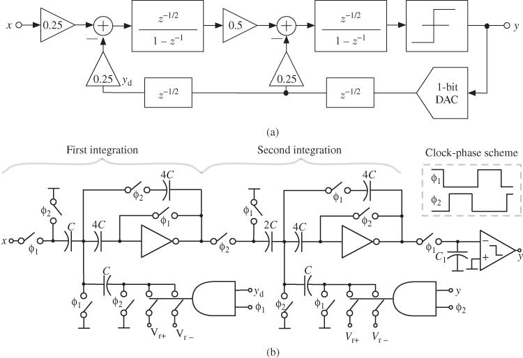
However, despite the aforementioned benefits of replacing OTAs with digital-based circuit solutions, it should be noted that simple circuits such as inverters, cannot be seen as the panacea for all analog design problems in ![]() Ms. In practice, there is always a trade-off between the required electrical performance of a given building block and the circuit complexity in terms of number of transistors, with the subsequent penalty in power consumption, silicon area, impact of parasitics, etc. Therefore, a simple inverter circuit cannot replace a high-performance OTA. However, depending on the modulator specifications and target application, digital-based integrators could be a suited circuit solution. For instance, this might be the case in some biomedical applications demanding very low power consumption and/or wideband applications requiring ultra-high-speed loop-filter circuits. In both cases, the required DR is typically below 60–70 dB, which might not be very demanding in terms of finite DC gain of loop-filter building blocks and, consequently, the use of simple digital-based circuit solutions may result competitive. Nevertheless, the use of digital techniques is still at an early stage and it is expected that circuit improvements derived from technology downscaling will make possible that
Ms. In practice, there is always a trade-off between the required electrical performance of a given building block and the circuit complexity in terms of number of transistors, with the subsequent penalty in power consumption, silicon area, impact of parasitics, etc. Therefore, a simple inverter circuit cannot replace a high-performance OTA. However, depending on the modulator specifications and target application, digital-based integrators could be a suited circuit solution. For instance, this might be the case in some biomedical applications demanding very low power consumption and/or wideband applications requiring ultra-high-speed loop-filter circuits. In both cases, the required DR is typically below 60–70 dB, which might not be very demanding in terms of finite DC gain of loop-filter building blocks and, consequently, the use of simple digital-based circuit solutions may result competitive. Nevertheless, the use of digital techniques is still at an early stage and it is expected that circuit improvements derived from technology downscaling will make possible that ![]() Ms become more and more digital in a near future.
Ms become more and more digital in a near future.
5.3.6 Adaptive/Reconfigurable  Ms
Ms
The integration of entire wireless telecom systems into mainstream low-cost digitally oriented nanometer CMOS technologies together with the continuous increasing number of standards, operation modes, and applications, is driving the need of the so-called adaptive/reconfigurable ADCs, which are a particular kind of ADC that can reconfigure its performance metrics to different sets of specifications with adaptive power consumption. However, the practical implementation of this kind of ADCs involves a number of practical issues and trade-offs at both architecture and circuit level, which must be taken into account to optimize the performance in terms of power budget. This problem is indeed aggravated as efficiency is required in an increasingly wide tunable region in the resolution-versus-bandwidth plane.
In this application scenario, ![]() Ms are very suited for the implementation of this kind of ADC as the variation of their basic parameters—OSR,
Ms are very suited for the implementation of this kind of ADC as the variation of their basic parameters—OSR, ![]() , and
, and ![]() —can easily contribute to adapting the ADC performance to different requirements with optimized power consumption and large hardware reuse [321].
—can easily contribute to adapting the ADC performance to different requirements with optimized power consumption and large hardware reuse [321].
Reconfiguration at Architecture Level
The aforementioned reasons explain why state-of-the-art multistandard, multimode ADCs have been mainly implemented using ![]() Ms. Indeed, a number of adaptive/reconfigurable
Ms. Indeed, a number of adaptive/reconfigurable ![]() M ICs have been reported in the literature, implemented with both SC and CT circuit techniques, as summarized in Tables 5.12 and 5.13, respectively. The majority of the
M ICs have been reported in the literature, implemented with both SC and CT circuit techniques, as summarized in Tables 5.12 and 5.13, respectively. The majority of the ![]() Ms included in these tables are able to digitize more than three standards [85, 287–295, 297], achieving cutting-edge performance while digitizing signals with
Ms included in these tables are able to digitize more than three standards [85, 287–295, 297], achieving cutting-edge performance while digitizing signals with ![]() ranging from hundreds of kilohertz to tens of megahertz. Although changing the sampling frequency has been the reconfiguration strategy most commonly applied, the mandatory use of low values for OSR in wideband standards has forced
ranging from hundreds of kilohertz to tens of megahertz. Although changing the sampling frequency has been the reconfiguration strategy most commonly applied, the mandatory use of low values for OSR in wideband standards has forced ![]() Ms to achieve the required DR by resorting to different strategies, including adaptive high-order shaping [287, 292], switchable cascade topologies [290, 291, 297], multirating [290], programmable notches within the signal band [287, 300], and multibit embedded quantizers with adjustable number of bits [85].
Ms to achieve the required DR by resorting to different strategies, including adaptive high-order shaping [287, 292], switchable cascade topologies [290, 291, 297], multirating [290], programmable notches within the signal band [287, 300], and multibit embedded quantizers with adjustable number of bits [85].
Adaptation at Circuit Level
The mentioned architecture reconfiguration strategies are frequently combined with circuit/transistor-level techniques in order to increase the energy efficiency of adaptive/reconfigurable ![]() Ms. Among others, one of the most commonly used circuit techniques consists of implementing switchable unit cells, such as OTAs [295, 300], or unit capacitors [237, 298], in which a different number of unit elements is connected depending on the required electrical performance of a given
Ms. Among others, one of the most commonly used circuit techniques consists of implementing switchable unit cells, such as OTAs [295, 300], or unit capacitors [237, 298], in which a different number of unit elements is connected depending on the required electrical performance of a given ![]() M building block. Apart from the former circuit-level reconfiguration techniques, programmable bias current generators are frequently used in order to adapt the bias current and, subsequently, the power consumption of the amplifiers (and the preamplifiers used for the comparators) to the different operation modes covered by the reconfigurable
M building block. Apart from the former circuit-level reconfiguration techniques, programmable bias current generators are frequently used in order to adapt the bias current and, subsequently, the power consumption of the amplifiers (and the preamplifiers used for the comparators) to the different operation modes covered by the reconfigurable ![]() M [291, 298].
M [291, 298].
Concurrency
Although both single-loop and cascade topologies report state-of-the-art performance, cascade ![]() Ms are a priori more suitable architectures for the implementation of adaptive/reconfigurable ADCs. Indeed, the modular nature of cascade topologies allows to easily turn different stages either on or off depending on the loop-filter order
Ms are a priori more suitable architectures for the implementation of adaptive/reconfigurable ADCs. Indeed, the modular nature of cascade topologies allows to easily turn different stages either on or off depending on the loop-filter order ![]() required for a given set of specifications, while keeping system stability and low sensitivity to circuit nonidealities. In addition to reconfiguring its performance parameters, a multimode
required for a given set of specifications, while keeping system stability and low sensitivity to circuit nonidealities. In addition to reconfiguring its performance parameters, a multimode ![]() ADC must digitize signals corresponding to different standards in a parallel or concurrent way—that is, GSM and Bluetooth signals, and/or UMTS and WLAN signals.
ADC must digitize signals corresponding to different standards in a parallel or concurrent way—that is, GSM and Bluetooth signals, and/or UMTS and WLAN signals.
Concurrency can be easily implemented in a cascade ![]() M as conceptually illustrated in Figure 5.27, where a concurrent switchable network is used for allowing the modulator to be configured as several submodulators working in parallel, each one processing a different input signal. A number of control signals are needed to enable the switches that correspond to the desired operation mode in each case, either concurrent or cascaded. Moreover, a programmable DCL is required, which should be adapted to the concurrent operation and/or the number of stages working as either isolated single-loop modulators or as parts of a cascade. The price to pay is an increase in the complexity of the digital control circuits as compared to conventional
M as conceptually illustrated in Figure 5.27, where a concurrent switchable network is used for allowing the modulator to be configured as several submodulators working in parallel, each one processing a different input signal. A number of control signals are needed to enable the switches that correspond to the desired operation mode in each case, either concurrent or cascaded. Moreover, a programmable DCL is required, which should be adapted to the concurrent operation and/or the number of stages working as either isolated single-loop modulators or as parts of a cascade. The price to pay is an increase in the complexity of the digital control circuits as compared to conventional ![]() Ms. However, the implementation of digital circuits benefits from technology downscaling, which may result in a more efficient solution than using separate ADCs operating in parallel. Thus, the majority of state-of-the-art reconfigurable
Ms. However, the implementation of digital circuits benefits from technology downscaling, which may result in a more efficient solution than using separate ADCs operating in parallel. Thus, the majority of state-of-the-art reconfigurable ![]() Ms focus their efficiency in achieving reconfigurability and adaptability. The increasing need of implementing concurrency in modern mobile handheld terminals has motivated doing more research on this topic and the first experimental evidences of implementing this feature have already been reported [322].
Ms focus their efficiency in achieving reconfigurability and adaptability. The increasing need of implementing concurrency in modern mobile handheld terminals has motivated doing more research on this topic and the first experimental evidences of implementing this feature have already been reported [322].
Figure 5.27 Conceptual block diagram of a reconfigurable cascade ![]() M with concurrent operation.
M with concurrent operation.

5.3.7 Ultra-High-Speed CT- Ms for RF Digitization
As previously explained in this chapter, more and more CT-![]() Ms are demonstrating to be a competitive solution for the implementation of power-efficient ADCs operating in the gigahertz range [154, 161, 181, 207, 232, 239, 251, 323]. This feature has prompted the interest of RF circuit designers to use CT-
Ms are demonstrating to be a competitive solution for the implementation of power-efficient ADCs operating in the gigahertz range [154, 161, 181, 207, 232, 239, 251, 323]. This feature has prompted the interest of RF circuit designers to use CT-![]() Ms in digital-intensive RF transceivers. Thus, in addition to digitize signals, CT-
Ms in digital-intensive RF transceivers. Thus, in addition to digitize signals, CT-![]() M ICs might take advantage of their CT circuit nature to merge some RF functionalities such as blocker-rejection filtering, frequency-mixing process, channel-selection and antialiasing filtering, and so on [155, 176, 203, 233, 284]. All these functionalities can be embedded within the
M ICs might take advantage of their CT circuit nature to merge some RF functionalities such as blocker-rejection filtering, frequency-mixing process, channel-selection and antialiasing filtering, and so on [155, 176, 203, 233, 284]. All these functionalities can be embedded within the ![]() M feedback loop as conceptually depicted in Figure 5.28a, thus resulting in more compact RF receivers, with a reduced complexity in the analog hardware and the subsequent benefits in terms of sensitivity to circuit imperfections and power/area scalability with technology.
M feedback loop as conceptually depicted in Figure 5.28a, thus resulting in more compact RF receivers, with a reduced complexity in the analog hardware and the subsequent benefits in terms of sensitivity to circuit imperfections and power/area scalability with technology.
Figure 5.28 Conceptual block diagrams of digital-intensive RF receivers using: (a) reconfigurable LP/BP-![]() M with embedded analog baseband signal conditioning. The
M with embedded analog baseband signal conditioning. The ![]() M can be implemented using either SC or CT circuits depending on the operating frequency. (b) RF-to-baseband CT BP-
M can be implemented using either SC or CT circuits depending on the operating frequency. (b) RF-to-baseband CT BP-![]() M, where RF signals are directly digitized and most signal processing is implemented by the DSP.
M, where RF signals are directly digitized and most signal processing is implemented by the DSP.

A fully digitized RF receiver, conceptually illustrated in Figure 5.28b, should place the analog-to-digital interface as close as possible to the antenna—an approach commonly referred to as RF-to-baseband digitization or RF-to-digital conversion [251]. Although this is the ideal implementation of the so-called software-defined radio (SDR) paradigm [324], its practical application scenario is still far from a consumer product deployment. This is mostly limited by the unfeasible power-hungry requirements demanded by the ADC, particularly in terms of signal bandwidth, linearity, and dynamic range, supporting signal levels from the sensitivity to the full strength. In order to reduce the power consumption, some authors propose using BP-![]() Ms to digitize IF signals [232, 236], by implementing an IF-digitization scheme as that shown in Figure 5.28a. This way, after being preamplified by the LNA and downconverted from RF to IF in the mixer, the incoming signal is digitized by a CT BP-
Ms to digitize IF signals [232, 236], by implementing an IF-digitization scheme as that shown in Figure 5.28a. This way, after being preamplified by the LNA and downconverted from RF to IF in the mixer, the incoming signal is digitized by a CT BP-![]() M. A good example of this compact and power-efficient solution is reported by Harrison et al. in [232]. The modulator is integrated in a 40-nm CMOS technology and digitizes 20-MHz signals placed at 700–800 MHz with 70-dB SNDR, dissipating 20 mW when clocked at 3.2 GHz.
M. A good example of this compact and power-efficient solution is reported by Harrison et al. in [232]. The modulator is integrated in a 40-nm CMOS technology and digitizes 20-MHz signals placed at 700–800 MHz with 70-dB SNDR, dissipating 20 mW when clocked at 3.2 GHz.
In spite of the strong specifications required by RF-to-digital converters, the recent advances in BP-![]() M ICs—particularly some ICs implemented using CT circuits listed in Table 5.9—are pushing RF digitization forward, taking significant steps toward future implementations of SDR mobile devices based on the conceptual scheme of Figure 5.28a. It is interesting to note that one of the ICs in Table 5.9, reported by Martens et al. in [251], is clocked at 8.88 GHz, which is the highest sampling rate reported to date by CMOS
M ICs—particularly some ICs implemented using CT circuits listed in Table 5.9—are pushing RF digitization forward, taking significant steps toward future implementations of SDR mobile devices based on the conceptual scheme of Figure 5.28a. It is interesting to note that one of the ICs in Table 5.9, reported by Martens et al. in [251], is clocked at 8.88 GHz, which is the highest sampling rate reported to date by CMOS ![]() Ms. The chip presented in [251] is a fourth-order CT BP-
Ms. The chip presented in [251] is a fourth-order CT BP-![]() M with a notch-frequency placed at
M with a notch-frequency placed at ![]() , that is, 2.2 GHz. This high-speed operation can be achieved by combining six time-interleaving quantizers with a polyphase decimation filter, which allows RF digitization at 2.2 GHz with 48-dB DR within 80-MHz bandwidth, while consuming 164 mW.
, that is, 2.2 GHz. This high-speed operation can be achieved by combining six time-interleaving quantizers with a polyphase decimation filter, which allows RF digitization at 2.2 GHz with 48-dB DR within 80-MHz bandwidth, while consuming 164 mW.
The majority of these state-of-the-art CT BP-![]() Ms intended for RF-to-baseband digitization use a fixed center frequency or notch frequency and combine diverse strategies to relax the ADC requirements—such as out-of-band embedded filtering [250] or subsampling [234]. A good example was proposed by Ryckaert et al., who reported the design of a six-order BP-
Ms intended for RF-to-baseband digitization use a fixed center frequency or notch frequency and combine diverse strategies to relax the ADC requirements—such as out-of-band embedded filtering [250] or subsampling [234]. A good example was proposed by Ryckaert et al., who reported the design of a six-order BP-![]() M—conceptually depicted in Figure 5.29—which uses the subsampling technique [325] for digitizing signals centered at 2.4 GHz with
M—conceptually depicted in Figure 5.29—which uses the subsampling technique [325] for digitizing signals centered at 2.4 GHz with ![]() GHz, that is, a ratio of
GHz, that is, a ratio of ![]() . The loop filter—implemented by Q-enhanced LC resonators—is made tunable by varying tank capacitors such that the operation of the ADC can be adjusted to the desired center frequency. However, a wider tuning range is required in order to implement an SDR receiver.
. The loop filter—implemented by Q-enhanced LC resonators—is made tunable by varying tank capacitors such that the operation of the ADC can be adjusted to the desired center frequency. However, a wider tuning range is required in order to implement an SDR receiver.
Figure 5.29 Example of a six-order Gm-LC BP-![]() M for RF digitization proposed by Ryckaert et al. [234]. It combines subsampling and two time-interleaved comparators to digitize 60-MHz signals placed at 2.4 GHz when clocked at 3 GHz.
M for RF digitization proposed by Ryckaert et al. [234]. It combines subsampling and two time-interleaved comparators to digitize 60-MHz signals placed at 2.4 GHz when clocked at 3 GHz.

Indeed, one of the problems associated with conventional BP-![]() Ms with a fixed notch-frequency is that the RF receiver requires a programmable frequency synthesizer (Figure 5.28) in order to place the signal band within the pass-band of the BP-
Ms with a fixed notch-frequency is that the RF receiver requires a programmable frequency synthesizer (Figure 5.28) in order to place the signal band within the pass-band of the BP-![]() M. This issue has motivated the interest for reconfigurable BP-
M. This issue has motivated the interest for reconfigurable BP-![]() Ms with wide tunable notch-frequency. On the basis of this strategy, Yamamoto et al. reported in [326] one of the widest tuning ranges for the notch-frequency achieved by SC BP-
Ms with wide tunable notch-frequency. On the basis of this strategy, Yamamoto et al. reported in [326] one of the widest tuning ranges for the notch-frequency achieved by SC BP-![]() Ms, ranging from DC to 12.6 MHz. This tuning range can be significantly increased by using CT-
Ms, ranging from DC to 12.6 MHz. This tuning range can be significantly increased by using CT-![]() Ms, as reported by Shibata et al. in [239], where a sixth-order reconfigurable LP/BP-
Ms, as reported by Shibata et al. in [239], where a sixth-order reconfigurable LP/BP-![]() M IC features a DC-to-1 GHz tunable notch-frequency, at the price of consuming 550 mW.
M IC features a DC-to-1 GHz tunable notch-frequency, at the price of consuming 550 mW.
Another interesting approach of using CT BP-![]() Ms with a reconfigurable 0.8–2 GHz notch-frequency was reported by Gupta et al. in [253, 323]. In this case, a second-order topology is integrated together with a quadrature phase-locked loop (QPLL) to allow quadrature phase synchronization between a raised-cosine feedback DAC and the embedded quantizer. As shown in Table 5.9, the chip digitizes 1-MHz signals placed at 797 MHz with a DR of 8.3 bit, while consuming 41 mW, out of which 11 mW are consumed by the QPLL.
Ms with a reconfigurable 0.8–2 GHz notch-frequency was reported by Gupta et al. in [253, 323]. In this case, a second-order topology is integrated together with a quadrature phase-locked loop (QPLL) to allow quadrature phase synchronization between a raised-cosine feedback DAC and the embedded quantizer. As shown in Table 5.9, the chip digitizes 1-MHz signals placed at 797 MHz with a DR of 8.3 bit, while consuming 41 mW, out of which 11 mW are consumed by the QPLL.
In conclusion, the trend toward RF digitization is expected to continue, as revealed by the increasing number of CT BP-![]() Ms operating in the gigahertz range that are becoming commonplace. The main issue of this approach is the power consumption that must be reduced in order to be competitive with conventional approaches based on a direct-conversion receiver made up of an analog signal conditioning (basically an LNA, a mixer, and a baseband filter) followed by a reconfigurable LP-
Ms operating in the gigahertz range that are becoming commonplace. The main issue of this approach is the power consumption that must be reduced in order to be competitive with conventional approaches based on a direct-conversion receiver made up of an analog signal conditioning (basically an LNA, a mixer, and a baseband filter) followed by a reconfigurable LP-![]() M [321].
M [321].
5.4 Classification of State-of-the-Art References
For the sake of clarity, this chapter is concluded by grouping the references on the state-of-the-art ![]() M ICs, according to the same classification criteria followed in Tables 5.13:
M ICs, according to the same classification criteria followed in Tables 5.13:
- SC single-loop single-bit LP-
 Ms: [12–54]
 - SC single-loop multibit LP-
 Ms: [22, 55–98]
 - SC cascade single-bit LP-
 Ms: [19, 99–116]
 - SC cascade multibit LP-
 Ms: [38, 76, 110, 117–136]
 - SC BP-
 Ms: [137–153]
 - CT single-loop single-bit LP-
 Ms: [154–192]
 - CT single-loop multibit LP-
 Ms: [193–226]
 - CT cascade LP-
 Ms: [227–231, 297]
 - CT BP-
 Ms: [232–258]
  Ms with time-coded quantization: [259–268]
- Hybrid
 Ms: [215, 228, 269–286]
 - SC reconfigurable
 Ms: [85, 287–291, 300]
 - CT reconfigurable
 Ms: [292–299].
5.5 Summary
This chapter presented an analysis of the state of the art on CMOS ![]() Ms, making a systematic classification of their architectures, circuit techniques, and target applications. On the basis of the practical approach followed in this book, the empirical data extracted from this statistical survey has been applied to identify design trends and challenges in order to help designers select the most suitable
Ms, making a systematic classification of their architectures, circuit techniques, and target applications. On the basis of the practical approach followed in this book, the empirical data extracted from this statistical survey has been applied to identify design trends and challenges in order to help designers select the most suitable ![]() M among different families for a given application and/or range of specifications. With this practical objective in mind, a number of design trade-offs have been discussed at different abstraction levels, namely architecture level (i.e., single-loop vs cascade, single-bit vs multibit, low-pass vs band-pass), circuit-level (i.e., SC vs CT, Gm-C vs active-RC), and technology process. The conclusions derived from the presented statistical and empirical analysis can be used as a practical guide to be incorporated in the top-down/bottom-up systematic design procedure described in this book.
M among different families for a given application and/or range of specifications. With this practical objective in mind, a number of design trade-offs have been discussed at different abstraction levels, namely architecture level (i.e., single-loop vs cascade, single-bit vs multibit, low-pass vs band-pass), circuit-level (i.e., SC vs CT, Gm-C vs active-RC), and technology process. The conclusions derived from the presented statistical and empirical analysis can be used as a practical guide to be incorporated in the top-down/bottom-up systematic design procedure described in this book.
The chapter is concluded with a review of cutting-edge ![]() M ICs, considering diverse circuits and systems techniques, namely: advanced cascade topologies, hybrid implementations, MR architectures, time-coded quantization, digital-based loop-filter implementations, adaptive/reconfigurable architectures, and ultra-high-speed
M ICs, considering diverse circuits and systems techniques, namely: advanced cascade topologies, hybrid implementations, MR architectures, time-coded quantization, digital-based loop-filter implementations, adaptive/reconfigurable architectures, and ultra-high-speed ![]() Ms.
Ms.
As a final conclusion, it could be said that compared to other kinds of ADCs, ![]() M techniques cover the widest resolution-versus-bandwidth region, targeting more and more applications and taking advantage of CMOS technology downscaling. This trend is expected to continue with the development and improvement of some architecture and circuit techniques—particularly using CT circuits, time-code quantization, and an intensive use of digital-assisted analog circuits—which will all push
M techniques cover the widest resolution-versus-bandwidth region, targeting more and more applications and taking advantage of CMOS technology downscaling. This trend is expected to continue with the development and improvement of some architecture and circuit techniques—particularly using CT circuits, time-code quantization, and an intensive use of digital-assisted analog circuits—which will all push ![]() Ms forward, increasing their dominance in a growing number of data-conversion applications.
Ms forward, increasing their dominance in a growing number of data-conversion applications.
References
[1] P. M. Aziz et al., “An Overview of Sigma-Delta Converters,” IEEE Signal Processing Magazine, vol. 13, pp. 61–84, January 1996.
[2] R. Schreier and G. C. Temes, Understanding Delta-Sigma Data Converters, IEEE Press, 2005.
[3] J. M. de la Rosa, “Sigma-Delta Modulators: Tutorial Overview, Design Guide, and State-of-the-Art Survey,” IEEE Transactions on Circuits and Systems I: Regular Papers, vol. 58, pp. 1–21, January 2011.
[4] R. H. Walden, “Analog-to-Digital Converter Survey and Analysis,” IEEE Journal on Selected Areas in Communications, vol. 17, pp. 539–550, April 1999.
[5] B. Murmann, “A/D Converter Trends: Power Dissipation, Scaling and Digitally Assisted Architectures,” Proc. of the IEEE Custom Integrated Circuits Conf., pp. 105–112, 2008.
[6] H. S. Lee and C. G. Sodini, “Analog-to-Digital Converters: Digitizing the Analog World,” Proceedings of the IEEE, vol. 96, pp. 323–334, February 2008.
[7] B. E. Jonsson, “On CMOS Scaling and A/D-Converter Performance,” Proc. of the NORCHIP Conf., pp. 1–4, November 2010.
[8] B. E. Jonsson, “A Survey of A/D-Converter Performance Evolution,” Proc. of the IEEE Intl. Conf. on Electronics, Circuits, and Systems, pp. 766–769, December 2010.
[9] B. E. Jonsson, “An Empirical Approach to Finding Energy Efficient ADC Architectures,” Proc. of the Intl. Workshop on ADC Modeling, Testing and Data Converter Analysis and Design and IEEE ADC Forum, June 2011.
[10] G. Manganaro, Advanced Data Converters, Cambridge University Press, 2012.
[11] B. Murmann, ADC Performance Survey 1997–2012. [Online]. Available: http://www.stanford.edu/∼murmann/adcsurvey.html, 2012.
[12] Y. Chae and G. Han, “Low Voltage, Low Power, Inverter-Based Switched-Capacitor Delta-Sigma Modulator,” IEEE Journal of Solid-State Circuits, vol. 44, pp. 369–373, May 2009.
[13] J. Roh et al., “A 0.9-V 60-![]() W 1-Bit Fourth-Order Delta-Sigma Modulator With 83-dB Dynamic Range,” IEEE Journal of Solid-State Circuits, vol. 43, pp. 361–370, February 2008.
W 1-Bit Fourth-Order Delta-Sigma Modulator With 83-dB Dynamic Range,” IEEE Journal of Solid-State Circuits, vol. 43, pp. 361–370, February 2008.
[14] C. B. Wang et al., “A 113-dB DSD Audio ADC Using a Density-Modulated Dithering Scheme,” IEEE Journal of Solid-State Circuits, vol. 28, pp. 114–119, January 2003.
[15] L. Yao, M. Steyaert, and W. Sansen, “A 1-V 140-![]() W 88-dB Audio Sigma-Delta modulator in 90-nm CMOS,” IEEE Journal of Solid-State Circuits, vol. 39, pp. 1809–1818, November 2004.
W 88-dB Audio Sigma-Delta modulator in 90-nm CMOS,” IEEE Journal of Solid-State Circuits, vol. 39, pp. 1809–1818, November 2004.
[16] S. Gambini and J. Rabaey, “A 100 kS/S 65 dB DR ![]() ADC with 0.65V Supply Voltage,” Proc. of the IEEE European Solid-State Circuits Conf., pp. 202–205, September 2007.
ADC with 0.65V Supply Voltage,” Proc. of the IEEE European Solid-State Circuits Conf., pp. 202–205, September 2007.
[17] H. Park et al., “A 0.7-V 100-dB 870-![]() W Digital Audio
W Digital Audio ![]() Modulator,” IEEE Symp. VLSI Circuits. Digest of Technical Papers, pp. 178–179, 2008.
Modulator,” IEEE Symp. VLSI Circuits. Digest of Technical Papers, pp. 178–179, 2008.
[18] V. Peluso et al., “A 900-mV Low-Power ![]() A/D Converter with 77-dB Dynamic Range,” IEEE Journal of Solid-State Circuits, vol. 12, pp. 1887–1897, December 1998.
A/D Converter with 77-dB Dynamic Range,” IEEE Journal of Solid-State Circuits, vol. 12, pp. 1887–1897, December 1998.
[19] J. Sauerbrey et al., “0.65V Sigma-Delta Modulators,” Proc. of the IEEE Intl. Symp. on Circuits and Systems, pp. 1021–1024, May 2003.
[20] A. L. Coban and P. E. Allen, “A 1.5V 1.0 mW Audio ![]() Modulator with 98 dB Dynamic Range,” IEEE ISSCC Digest of Technical Papers pp. 50–51, February 1999.
Modulator with 98 dB Dynamic Range,” IEEE ISSCC Digest of Technical Papers pp. 50–51, February 1999.
[21] P. Rombouts et al., “A 250-kHz 94-dB Double-Sampling ![]() Modulation A/D Converter With a Modified Noise Transfer Function,” IEEE Journal of Solid-State Circuits, vol. 10, pp. 1657–1662, October 2003.
Modulation A/D Converter With a Modified Noise Transfer Function,” IEEE Journal of Solid-State Circuits, vol. 10, pp. 1657–1662, October 2003.
[22] J. Xu et al., “Power Optimization of High Performance ![]() Modulators for Portable ganesan Measurement Applications,” Proc. of the IEEE Asian Solid-State Circuits Conf., 2010.
Modulators for Portable ganesan Measurement Applications,” Proc. of the IEEE Asian Solid-State Circuits Conf., 2010.
[23] F. Michel and M. Steyaert, “A 250 mW 7.5![]() W 61 dB SNDR CMOS SC
W 61 dB SNDR CMOS SC ![]() Modulator Using a Near-Threshold-Voltage-Biased CMOS Inverter Technique,” IEEE ISSCC Digest of Technical Papers, pp. 476–477, February 2011.
Modulator Using a Near-Threshold-Voltage-Biased CMOS Inverter Technique,” IEEE ISSCC Digest of Technical Papers, pp. 476–477, February 2011.
[24] Z. Cao et al., “A 14 mW 2.5 MS/s 14 bit ![]() Modulator Using Split-Path Pseudo-Differential Amplifiers,” IEEE Journal of Solid-State Circuits, vol. 42, pp. 2169–2179, October 2007.
Modulator Using Split-Path Pseudo-Differential Amplifiers,” IEEE Journal of Solid-State Circuits, vol. 42, pp. 2169–2179, October 2007.
[25] N. Klemmer and E. Hegazi, “A DLL-Biased, 14-Bit ΔΣ Analog-to-Digital Converter for GSM/GPRS/EDGE Handsets,” IEEE Journal of Solid-State Circuits, vol. 41, pp. 330–338, February 2006.
[26] K. A. Donoghue et al., “A Digitally Calibrated 5-mW 2-MS/s 4th-Order ![]() ADC in 0.25-
ADC in 0.25-![]() m CMOS with 94 dB SFDR,” Proc. of the IEEE European Solid-State Circuits Conf., pp. 422–425, September 2010.
m CMOS with 94 dB SFDR,” Proc. of the IEEE European Solid-State Circuits Conf., pp. 422–425, September 2010.
[27] B. Nowacki et al., “A 1.2V 300![]() W Second-Order Switched-Capacitor
W Second-Order Switched-Capacitor ![]() Modulator Using Ultra Incomplete Settling with 73 dB SNDR and 300 kHz BW in 130 nm CMOS,” Proc. of the IEEE European Solid-State Circuits Conf., pp. 271–274, September 2011.
Modulator Using Ultra Incomplete Settling with 73 dB SNDR and 300 kHz BW in 130 nm CMOS,” Proc. of the IEEE European Solid-State Circuits Conf., pp. 271–274, September 2011.
[28] F. Chen, S. Ramaswamy, and B. Bakkaloglu, “A 1.5V 1 mA 80 dB Passive ![]() ADC in 0.13
ADC in 0.13![]() m Digital CMOS Process,” IEEE ISSCC Digest of Technical Papers, vol. 54-55, pp. 244–245, February 2003.
m Digital CMOS Process,” IEEE ISSCC Digest of Technical Papers, vol. 54-55, pp. 244–245, February 2003.
[29] M. Dessouky and A. Kaiser, “Very Low-Voltage Digital-Audio ![]() Modulator with 88-dB Dynamic Range Using Local Switch Bootstrapping,” IEEE Journal of Solid-State Circuits, vol. 36, pp. 349–355, March 2001.
Modulator with 88-dB Dynamic Range Using Local Switch Bootstrapping,” IEEE Journal of Solid-State Circuits, vol. 36, pp. 349–355, March 2001.
[30] Y. Chae et al., “A 0.7V 36![]() W 85 dB-DR Audio
W 85 dB-DR Audio ![]() Modulator Using Class-C Inverter,” IEEE ISSCC Digest of Technical Papers, pp. 490–491, February 2008.
Modulator Using Class-C Inverter,” IEEE ISSCC Digest of Technical Papers, pp. 490–491, February 2008.
[31] T. Musah et al., “A 630![]() W Zero-Crossing-Based
W Zero-Crossing-Based ![]() ADC Using Switched-Resistor Current Sources in 45 nm CMOS,” Proc. of the IEEE Custom Integrated Circuits Conf., September 2009.
ADC Using Switched-Resistor Current Sources in 45 nm CMOS,” Proc. of the IEEE Custom Integrated Circuits Conf., September 2009.
[32] J. Sauerbrey et al., “A 0.7-V MOSFET-Only Switched-Opamp ![]() Modulator in Standard Digital CMOS Technology,” IEEE Journal of Solid-State Circuits, vol. 37, pp. 1662–1669, December 2002.
Modulator in Standard Digital CMOS Technology,” IEEE Journal of Solid-State Circuits, vol. 37, pp. 1662–1669, December 2002.
[33] M. Snoeij et al., “A 4th-Order Switched-Capacitor Sigma-Delta A/D Converter Using a High-Ripple Chebyshev Loop Filter,” Proc. of the IEEE Intl. Symp. on Circuits and Systems, pp. 615–618, May 2001.
[34] J. Wang et al., “A 0.5V Feedforward Delta-Sigma Modulator with Inverter-Based Integrator,” Proc. of the IEEE European Solid-State Circuits Conf., September 2009.
[35] F. Medeiro et al., “Quick Design of High-Performance ![]() Modulators using CAD Tools: A 16.4 b 1.71 mW CMOS
Modulators using CAD Tools: A 16.4 b 1.71 mW CMOS ![]() M for 9.6 ksample/s A/D Conversion,” Proc. of 2nd IEEE-CAS Region 8 Workshop on Analog and Mixed IC Design), pp. 22–27, 1997.
M for 9.6 ksample/s A/D Conversion,” Proc. of 2nd IEEE-CAS Region 8 Workshop on Analog and Mixed IC Design), pp. 22–27, 1997.
[36] M. C. Huang and S. I. Lu, “A Fully Differential Comparator-Based Switched-Capacitor ![]() Modulator,” IEEE Journal of Solid-State Circuits, vol. 44, pp. 369–373, May 2009.
Modulator,” IEEE Journal of Solid-State Circuits, vol. 44, pp. 369–373, May 2009.
[37] V. Peluso et al., “A 1.5-V 100-![]() W
W ![]() Modulator with 12-b Dynamic Range Using the Switched-Opamp Technique,” IEEE Journal of Solid-State Circuits, vol. 32, pp. 943–952, July 1997.
Modulator with 12-b Dynamic Range Using the Switched-Opamp Technique,” IEEE Journal of Solid-State Circuits, vol. 32, pp. 943–952, July 1997.
[38] B. P. Brandt and B. A. Wooley, “A 50-MHz Multibit Sigma-Delta Modulator for 12-b 2-MHz A/D Conversion,” IEEE Journal of Solid-State Circuits, vol. 26, pp. 1746–1756, December 1991.
[39] T. Burger and Q. Huang, “A 13.5-mW 185-MSample/s ![]() Modulator for UMTS/GSM Dual-Standard IF Reception,” IEEE Journal of Solid-State Circuits, vol. 36, pp. 1868–1878, December 2001.
Modulator for UMTS/GSM Dual-Standard IF Reception,” IEEE Journal of Solid-State Circuits, vol. 36, pp. 1868–1878, December 2001.
[40] D. Senderowicz et al., “Low-Voltage Double-Sampled ![]() Converters,” IEEE Journal of Solid-State Circuits, vol. 32, pp. 1907–1919, December 1997.
Converters,” IEEE Journal of Solid-State Circuits, vol. 32, pp. 1907–1919, December 1997.
[41] S. Au and B. H. Leung, “A 1.95-V, 0.34-mW, 12-b Sigma-Delta Modulator Stabilized by Local Feedback Loops,” IEEE Journal of Solid-State Circuits, vol. 32, pp. 321–328, March 1997.
[42] J. Gilo et al., “A 1.8V 94 dB Dynamic Range ![]() Modulator for Voice Applications,” IEEE ISSCC Digest of Technical Papers, pp. 230–231, February 1996.
Modulator for Voice Applications,” IEEE ISSCC Digest of Technical Papers, pp. 230–231, February 1996.
[43] T. Tille and R. Meyer, “A 1.8-V MOSFET-Only ![]() Modulator Using Substrate Biased Depletion-Mode MOS Capacitors in Series Compensation,” IEEE Journal of Solid-State Circuits, vol. 36, pp. 1041–1047, July 2001.
Modulator Using Substrate Biased Depletion-Mode MOS Capacitors in Series Compensation,” IEEE Journal of Solid-State Circuits, vol. 36, pp. 1041–1047, July 2001.
[44] P. Maulik et al., “A 16-Bit 250-kHz Delta-Sigma Modulator and Decimation Filter,” IEEE Journal of Solid-State Circuits, vol. 35, pp. 458–467, April 2000.
[45] A. Gerosa et al., “A Fully-Integrated Two-Channel A/D Interface for hate Acquisition of Cardiac Signals in Implantable ganesan Pacemakers,” Proc. of the IEEE European Solid-State Circuits Conf., pp. 157–160, September 2003.
[46] C. Thanh et al., “A Second-Order Double-Sampled Delta-Sigma Modulator Using Individual-Level Averaging,” IEEE Jounal of Solid-State Circuits, vol. 32, pp. 1269–1273, August 1997.
[47] M. Keskin et al., “A 1-V 10-MHz Clock-Rate 13-Bit CMOS ![]() Modulator Using Unity-Gain-Reset Opamps,” IEEE Journal of Solid-State Circuits, vol. 37, pp. 817–824, July 2002.
Modulator Using Unity-Gain-Reset Opamps,” IEEE Journal of Solid-State Circuits, vol. 37, pp. 817–824, July 2002.
[48] D. A. Kerth et al., “A 120-dB Linear Switched-Capacitor Delta-Sigma Modulator,” IEEE ISSCC Digest of Technical Papers, pp. 196–197, February 1994.
[49] D. B. Kasha et al., “A 16-mW, 120-dB Linear Switched-Capacitor Delta-Sigma Modulator With Dynamic Biasing,” IEEE Journal of Solid-State Circuits, vol. 34, pp. 921–926, July 1999.
[50] F. Op't Eynde et al., “A CMOS Fourth-Order 14 b 500 k-Sample/s Sigma-Delta ADC Converter,” IEEE ISSCC Digest of Technical Papers, pp. 62–63, February 1991.
[51] H.-B. Le et al., “A Regulator-Free 84 dB DR Audio-Band ADC for Compact Digital Microphones,” Proc. of the IEEE Asian Solid-State Circuits Conf., 2010.
[52] B. E. Boser and B. A. Wooley, “The Design of Sigma-Delta Modulation Analog-to-Digital Converters,” IEEE Journal of Solid-State Circuits, vol. 23, pp. 1298–1308, December 1988.
[53] S. Nadeem et al., “16-Channel Oversampled Analog-to-Digital Converter,” IEEE Journal of Solid-State Circuits, vol. 29, pp. 1077–1085, September 1994.
[54] T. V. Burmas et al., “A Second-Order Double-Sampled Delta-Sigma Modulator Using Additive-Error Switching,” IEEE Journal of Solid-State Circuits, vol. 31, pp. 284–293, March 1996.
[55] A. Pena-Perez et al., “A 84 dB SNDR 100 kHz Bandwidth Low-Power Single Op-Amp Third-Order ![]() Modulator Consuming 140
Modulator Consuming 140![]() W,” IEEE ISSCC Digest of Technical Papers, pp. 478–479, February 2011.
W,” IEEE ISSCC Digest of Technical Papers, pp. 478–479, February 2011.
[56] Z. Yang et al., “A 0.5-V 35-![]() W 85-dB DR Double-Sampled
W 85-dB DR Double-Sampled ![]() Modulator for Audio Applications,” IEEE Journal of Solid-State Circuits, vol. 47, pp. 722–735, March 2012.
Modulator for Audio Applications,” IEEE Journal of Solid-State Circuits, vol. 47, pp. 722–735, March 2012.
[57] L. Liu et al., “A 95 dB SNDR Audio ![]() Modulator in 65 nm CMOS,” Proc. of the IEEE Custom Integrated Circuits Conf., September 2011.
Modulator in 65 nm CMOS,” Proc. of the IEEE Custom Integrated Circuits Conf., September 2011.
[58] N. Maghari and U.-K. Moon, “A Third-Order DT ![]() Modulator Using Noise-Shaped Bi-Directional Single-Slope Quantizer,” IEEE Journal of Solid-State Circuits, vol. 46, pp. 2882–2891, December 2011.
Modulator Using Noise-Shaped Bi-Directional Single-Slope Quantizer,” IEEE Journal of Solid-State Circuits, vol. 46, pp. 2882–2891, December 2011.
[59] K. Lee et al., “A Power-Efficient Two-Channel Time-Interleaved ![]() Modulator for Broadband Applications,” IEEE Journal of Solid-State Circuits, vol. 42, pp. 1206–1215, June 2007.
Modulator for Broadband Applications,” IEEE Journal of Solid-State Circuits, vol. 42, pp. 1206–1215, June 2007.
[60] L. Liu et al., “A 1-V 15-Bit Audio ![]() -ADC in 0.18
-ADC in 0.18![]() m CMOS,” IEEE Transactions on Circuits and Systems I—Regular Papers, vol. 59, pp. 915–925, May 2012.
m CMOS,” IEEE Transactions on Circuits and Systems I—Regular Papers, vol. 59, pp. 915–925, May 2012.
[61] H. Park et al., “A 0.7-V 870-![]() W Digital-Audio CMOS Sigma-Delta Modulator,” IEEE Journal of Solid-State Circuits, vol. 44, pp. 1078–1088, April 2009.
W Digital-Audio CMOS Sigma-Delta Modulator,” IEEE Journal of Solid-State Circuits, vol. 44, pp. 1078–1088, April 2009.
[62] K. Lee et al., “A Noise-Coupled Time-Interleaved ![]() ADC with 4.2 MHz BW, -98 dB THD, and 79 dB SNDR,” IEEE ISSCC Digest of Technical Papers, pp. 494–495, February 2008.
ADC with 4.2 MHz BW, -98 dB THD, and 79 dB SNDR,” IEEE ISSCC Digest of Technical Papers, pp. 494–495, February 2008.
[63] J. Koh, Y. Choi, and G. Gómez, “A 66 dB DR 1.2V 1.2 mW Single-Amplifier Double-Sampling 2nd-order ![]() ADC for WCDMA in 90 nm CMOS,” IEEE ISSCC Digest of Technical Papers, pp. 170–171, February 2005.
ADC for WCDMA in 90 nm CMOS,” IEEE ISSCC Digest of Technical Papers, pp. 170–171, February 2005.
[64] S. Kwon and F. Maloberti, “A 14 mW Multi-bit ![]() Modulator with 82 dB SNR and 86 dB DR for ADSL2+,” IEEE ISSCC Digest of Technical Papers, pp. 161–162, February 2006.
Modulator with 82 dB SNR and 86 dB DR for ADSL2+,” IEEE ISSCC Digest of Technical Papers, pp. 161–162, February 2006.
[65] K. Lee et al., “An 8.1-mW, 82 dB Delta-Sigma ADC with 1.9-MHz BW and –98 dB THD,” IEEE Journal of Solid-State Circuits, vol. 44, pp. 2202–2211, August 2009.
[66] L. Liu et al., “A 1V 350![]() W 92 dB SNDR 24 kHz
W 92 dB SNDR 24 kHz ![]() Modulator in 0.18
Modulator in 0.18![]() m CMOS,” Proc. of the IEEE Asian Solid-State Circuits Conf., 2010.
m CMOS,” Proc. of the IEEE Asian Solid-State Circuits Conf., 2010.
[67] N. Maghari et al., “A +5 dBFS Third-Order Extended Dynamic Range Single-Loop ![]() Modulator,” Proc. of the IEEE Custom Integrated Circuits Conf., September 2010.
Modulator,” Proc. of the IEEE Custom Integrated Circuits Conf., September 2010.
[68] K. Tiew et al., “A 0.06-mm![]() Double-Sampling Single-OTA 2nd-Order
Double-Sampling Single-OTA 2nd-Order ![]() Modulator in 0.18-
Modulator in 0.18-![]() m CMOS Technology,” Proc. of the IEEE Asian Solid-State Circuits Conf., 2011.
m CMOS Technology,” Proc. of the IEEE Asian Solid-State Circuits Conf., 2011.
[69] R. Gaggl, M. Inversi, and A. Wiesbauer, “A Power Optimized 14-Bit SC ![]() Modulator for ADSL CO Applications,” IEEE ISSCC Digest of Technical Papers, pp. 82–83, February 2004.
Modulator for ADSL CO Applications,” IEEE ISSCC Digest of Technical Papers, pp. 82–83, February 2004.
[70] J. Chae et al., “A 63 dB 16 mW 20 MHz BW Double-Sampled ![]() Analog-to-Digital Converter with An Embedded-Adder Quantizer,” Proc. of the IEEE Custom Integrated Circuits Conf., September 2010.
Analog-to-Digital Converter with An Embedded-Adder Quantizer,” Proc. of the IEEE Custom Integrated Circuits Conf., September 2010.
[71] Y. Wang et al., “A 2.5MHz BW and 78 dB SNDR Delta-Sigma Modulator Using Dynamically Biased Amplifiers,” Proc. of the IEEE Custom Integrated Circuits Conf., September 2008.
[72] E. Bonizzoni et al., “Third-Order ![]() Modulator with 61-dB SNR and 6-MHz Bandwidth Consuming 6 mW,” Proc. of the IEEE European Solid-State Circuits Conf., pp. 218–221, September 2008.
Modulator with 61-dB SNR and 6-MHz Bandwidth Consuming 6 mW,” Proc. of the IEEE European Solid-State Circuits Conf., pp. 218–221, September 2008.
[73] R. Reutemann, P. Balmelli, and Q. Huang, “A 33 mW 14 b 2.5 MSample/s ![]() A/D Converter in 0.25
A/D Converter in 0.25![]() m Digital CMOS,” IEEE ISSCC Digest of Technical Papers, vol. 1, p. 316, 2002.
m Digital CMOS,” IEEE ISSCC Digest of Technical Papers, vol. 1, p. 316, 2002.
[74] Y. Fujimoto et al., “A 100 MS/s 4 MHz Bandwidth 70 dB SNR ![]() ADC in 90 nm CMOS,” IEEE Journal of Solid-State Circuits, vol. 44, pp. 1697–1708, June 2009.
ADC in 90 nm CMOS,” IEEE Journal of Solid-State Circuits, vol. 44, pp. 1697–1708, June 2009.
[75] P. Balmelli and Q. Huang, “A 25-MS/s 14-b 200-mW ![]() Modulator in 0.18-
Modulator in 0.18-![]() m CMOS,” IEEE Journal of Solid-State Circuits, vol. 39, pp. 2161–2169, December 2004.
m CMOS,” IEEE Journal of Solid-State Circuits, vol. 39, pp. 2161–2169, December 2004.
[76] J. Yu and F. Maloberti, “A Low-Power Multi-Bit ![]() Modulator in 90-nm Digital CMOS Without DEM,” IEEE Journal of Solid-State Circuits, vol. 40, pp. 2428–2436, December 2005.
Modulator in 90-nm Digital CMOS Without DEM,” IEEE Journal of Solid-State Circuits, vol. 40, pp. 2428–2436, December 2005.
[77] G. Gomez and B. Haroun, “A 1.5V 2.4/2.9 mW 79/50 dB DR ![]() Modulator for GSM/WCDMA in a 0.14
Modulator for GSM/WCDMA in a 0.14![]() m Digital Process,” IEEE ISSCC Digest of Technical Papers, February 2002.
m Digital Process,” IEEE ISSCC Digest of Technical Papers, February 2002.
[78] M. G. Kim et al., “A 0.9 V 92 dB Double-Sampled Switched-RC Delta-Sigma Audio ADC,” IEEE Journal of Solid-State Circuits, vol. 43, pp. 1195–1206, May 2008.
[79] Y. Kim et al., “A 105.5 dB, 0.49 mm![]() Audio
Audio ![]() Modulator Using Chopper Stabilization and Fully Randomized DWA,” Proc. of the IEEE Custom Integrated Circuits Conf., September 2008.
Modulator Using Chopper Stabilization and Fully Randomized DWA,” Proc. of the IEEE Custom Integrated Circuits Conf., September 2008.
[80] R. Gaggl et al., “A 85-dB Dynamic Range Multibit Delta-Sigma ADC for ADSL-CO Applications in 0.18-![]() m CMOS,” IEEE Journal of Solid-State Circuits, vol. 38, pp. 1105–1114, July 2003.
m CMOS,” IEEE Journal of Solid-State Circuits, vol. 38, pp. 1105–1114, July 2003.
[81] J. Wu et al., “Multi-bit Sigma Delta ADC with Reduced Feedback Levels, Extended Dynamic Range and Increased Tolerance for Analog Imperfections,” Proc. of the IEEE Custom Integrated Circuits Conf., September 2007.
[82] Y. Geerts et al., “A High-Performance Multibit ![]() CMOS ADC,” IEEE Journal of Solid-State Circuits, vol. 35, pp. 1829–1840, December 1999.
CMOS ADC,” IEEE Journal of Solid-State Circuits, vol. 35, pp. 1829–1840, December 1999.
[83] J. Chen et al., “A 94 dB SFDR 78 dB DR 2.2MHz BW Multi-bit Delta-Sigma Modulator with Noise Shaping DAC,” Proc. of the IEEE Custom Integrated Circuits Conf., September 2007.
[84] A. J. Chen and Y. P. Xu, “Multibit Delta-Sigma Modulator With Noise-Shaping Dynamic Element Matching,” IEEE Journal of Solid-State Circuits, vol. 44, pp. 1125–1133, June 2009.
[85] M. R. Miller and C. S. Petrie, “A Multibit Sigma-Delta ADC for Multimode Receivers,” IEEE Journal of Solid-State Circuits, vol. 38, pp. 475–482, March 2003.
[86] Y. Yang et al., “A 114-dB 68-mW Chopper-Stabilized Stereo Multibit Audio ADC in 5.62 mm![]() ,” IEEE Journal of Solid-State Circuits, vol. 38, pp. 2061–2068, December 2003.
,” IEEE Journal of Solid-State Circuits, vol. 38, pp. 2061–2068, December 2003.
[87] O. Nys and R. K. Henderson, “A 19-bit Low-Power Multibit Sigma-Delta ADC Based on Data Weighted Averaging,” IEEE Journal of Solid-State Circuits, vol. 32, pp. 933–942, July 1997.
[88] T. Kuo et al., “A Wideband CMOS Sigma-Delta Modulator With Incremental Data Weighted Averaging,” IEEE Journal of Solid-State Circuits, vol. 37, pp. 11–17, January 2002.
[89] Y. Yang et al., “A Single Die 124 dB Stereo Audio Delta Sigma ADC With 111 dB THD,” Proc. of the IEEE European Solid-State Circuits Conf., pp. 252–255, September 2007.
[90] R. T. Baird et al., “A Low Oversampling Ratio 14-b 500-kHz ![]() ADC With a Self-Calibrated Multibit DAC,” IEEE Journal of Solid-State Circuits, vol. 31, pp. 312–320, March 1996.
ADC With a Self-Calibrated Multibit DAC,” IEEE Journal of Solid-State Circuits, vol. 31, pp. 312–320, March 1996.
[91] J. Johansson et al., “A 16-bit 60![]() W Multi-Bit
W Multi-Bit ![]() Modulator for Portable ECG Applications,” Proc. of the IEEE European Solid-State Circuits Conf., September 2003.
Modulator for Portable ECG Applications,” Proc. of the IEEE European Solid-State Circuits Conf., September 2003.
[92] J. Gilo et al., “A 5V, 118 dB ![]() Analog-to-Digital Converter for Wideband Digital Audio,” IEEE ISSCC Digest of Technical Papers, pp. 218–219, February 1997.
Analog-to-Digital Converter for Wideband Digital Audio,” IEEE ISSCC Digest of Technical Papers, pp. 218–219, February 1997.
[93] E. Fogleman and I. Galton, “A Dynamic Element Matching Technique for Reduced-Distortion Multibit Quantization in Delta-Sigma ADCs,” IEEE Transactions on Circuits and Systems—II: Analog and Digital Signal Processing, vol. 48, pp. 158–170, February 2001.
[94] E. Fogleman et al., “A 3.3-V Single-Poly CMOS Audio ADC Delta-Sigma Modulator with 98-dB Peak SINAD and 105-dB Peak SFDR,” IEEE Journal of Solid-State Circuits, vol. 35, pp. 297–307, March 2000.
[95] A. Prasad et al., “A 120 dB 300 mW Stereio Audio A/D Converter with 110 dB THD+N,” Proc. of the IEEE European Solid-State Circuits Conf., pp. 191–194, September 2004.
[96] F. Chen and B. H. Leung, “A High Resolution Multibit Sigma-Delta Modulator with Individual Level Averaging,” IEEE Journal of Solid-State Circuits, vol. 30, pp. 453–460, April 1995.
[97] J. Sauerbrey et al., “A Dual-Quantization Multi-Bit Sigma Delta Analog/Digital Converter,” Proc. of the IEEE Intl. Symp. on Circuits and Systems, pp. 437–440, May 1994.
[98] J. Xu et al., “A 9![]() W 88 dB DR Fully-Clocked Switched-Opamp
W 88 dB DR Fully-Clocked Switched-Opamp ![]() Modulator with Novel Power and Area Efficient Resonator,” Proc. of the IEEE Custom Integrated Circuits Conf., September 2011.
Modulator with Novel Power and Area Efficient Resonator,” Proc. of the IEEE Custom Integrated Circuits Conf., September 2011.
[99] L. Wang and L. Theogarajan, “An 18![]() W 79 dB-DR 20 kHz-BW MASH
W 79 dB-DR 20 kHz-BW MASH ![]() Modulator Utilizing Self-Biased Amplifiers for biomedical Applications,” Proc. of the IEEE Custom Integrated Circuits Conf., September 2011.
Modulator Utilizing Self-Biased Amplifiers for biomedical Applications,” Proc. of the IEEE Custom Integrated Circuits Conf., September 2011.
[100] K. A. Donoghue et al., “A Digitally Corrected 5-mW 2-MS/s SC ![]() ADC in 0.25-
ADC in 0.25-![]() m CMOS With 94-dB SFDR,” IEEE Journal of Solid-State Circuits, vol. 46, pp. 2673–2684, November 2011.
m CMOS With 94-dB SFDR,” IEEE Journal of Solid-State Circuits, vol. 46, pp. 2673–2684, November 2011.
[101] K. Cornelissens and M. Steyaert, “A 1-V 84-dB DR 1-MHz Bandwidth Cascade 3-1 Delta-Sigma ADC in 65-nm CMOS,” Proc. of the IEEE European Solid-State Circuits Conf., pp. 332–335, 2009.
[102] S. Rabii and B. A. Wooley, “A 1.8V Digital-Audio Sigma-Delta Modulator in 0.8![]() m CMOS,” IEEE Journal of Solid-State Circuits, vol. 32, pp. 783–796, June 1997.
m CMOS,” IEEE Journal of Solid-State Circuits, vol. 32, pp. 783–796, June 1997.
[103] C. Kuo et al., “A Low-Voltage Fourth-Order Cascade Delta-Sigma Modulator in 0.18-![]() m CMOS,” IEEE Journal of Solid-State Circuits, vol. 57, pp. 2450–2461, September 2010.
m CMOS,” IEEE Journal of Solid-State Circuits, vol. 57, pp. 2450–2461, September 2010.
[104] O. Oliaei et al., “A 5-mW Sigma-Delta Modulator With 84-dB Dynamic Range for GSM/EDGE,” IEEE Journal of Solid-State Circuits, vol. 37, pp. 2–10, January 2002.
[105] J. M. de la Rosa et al., “A CMOS 110-dB@40-kS/s Programmable-Gain Chopper-Stabilized Third-Order 2-1 Cascade Sigma-Delta Modulator for Low-Power High-Linearity Automotive Sensor ASICs,” IEEE Journal of Solid-State Circuits, vol. 40, pp. 2246–2264, November 2005.
[106] A. Morgado, R. del Río, and J. M. de la Rosa, “An Adaptive ![]() Modulator for Multi-Standard Hand-Held Wireless Devices,” Proc. of the IEEE Asian Solid-State Circuits Conf., pp. 232–235, 2007.
Modulator for Multi-Standard Hand-Held Wireless Devices,” Proc. of the IEEE Asian Solid-State Circuits Conf., pp. 232–235, 2007.
[107] Y. Geerts et al., “A 3.3-V, 15-bit, Delta-Sigma ADC with a Signal Bandwidth of 1.1 MHz for ADSL Applications,” IEEE Journal of Solid-State Circuits, vol. 34, pp. 1829–1840, July 1999.
[108] G. Yin et al., “A 16-b 320-kHz CMOS A/D Converter Using Two-Stage Third-Order ![]() Noise Shaping,” IEEE Journal of Solid-State Circuits, vol. 28, pp. 640–647, June 1993.
Noise Shaping,” IEEE Journal of Solid-State Circuits, vol. 28, pp. 640–647, June 1993.
[109] A. M. Marques et al., “A 15-b Resolution 2-MHz Nyquist Rate ![]() ADC in a 1-
ADC in a 1-![]() m CMOS Technology,” IEEE Journal of Solid-State Circuits, vol. 33, pp. 1065–1075, July 1998.
m CMOS Technology,” IEEE Journal of Solid-State Circuits, vol. 33, pp. 1065–1075, July 1998.
[110] J. C. Morizio et al., “14-bit 2.2-MS/s Sigma-Delta ADC's,” IEEE Journal of Solid-State Circuits, vol. 35, pp. 968–976, July 2000.
[111] G. J. Gomez, “A 102-dB Spurious-Free DR ![]() ADC Using a Dynamic Dither Scheme,” IEEE Journal of Solid-State Circuits, vol. 47, pp. 531–535, June 2000.
ADC Using a Dynamic Dither Scheme,” IEEE Journal of Solid-State Circuits, vol. 47, pp. 531–535, June 2000.
[112] L. A. Williams and B. A. Wooley, “A Third-Order Sigma-Delta Modulator with Extended Dynamic Range,” IEEE Journal of Solid-State Circuits, vol. 35, pp. 193–202, March 1994.
[113] C. B. Wang, “A 20-bit 25-kHz Delta-Sigma A/D Converter Utilizing a Frequency-Shaped Chopper Stabilization Scheme,” IEEE Journal of Solid-State Circuits, vol. 36, pp. 566–569, March 2001.
[114] M. Rebeschini, N. R. van Bavel, P. Rakers, R. Greene, J. Caldwell, and J. R. Haug, “A 16-b 160 kHz CMOS A/D Converter Using Sigma-Delta Modulation,” IEEE Journal of Solid-State Circuits, vol. 25, pp. 431–440, April 1990.
[115] I. Fujimori et al., “A 5-V Single-Chip Delta-Sigma Audio A/D Converter with 111 dB Dynamic Range,” IEEE Journal of Solid-State Circuits, vol. 32, pp. 329–336, March 1997.
[116] G. Miao et al., “An Oversampled A/D Converter Using Cascaded Fourth Order Sigma-Delta Modulation and Current Steering Logic,” Proc. of the IEEE Intl. Symp. on Circuits and Systems, pp. 412–415, May 1998.
[117] R. Zanbaghi et al., “A 75 dB SNDR, 10MHz Conversion Bandwidth Stage-Shared 2-2 MASH ![]() Modulator Dissipating 9 mW,” Proc. of the IEEE Custom Integrated Circuits Conf., September 2011.
Modulator Dissipating 9 mW,” Proc. of the IEEE Custom Integrated Circuits Conf., September 2011.
[118] P. Malla et al., “A 28 mW Spectrum-Sensing Reconfigurable 20MHz 72 dB-SNR 70 dB-SNDR DT ![]() ADC for 802.11 n/WiMAX Receivers,” IEEE ISSCC Digest of Technical Papers, February 2008.
ADC for 802.11 n/WiMAX Receivers,” IEEE ISSCC Digest of Technical Papers, February 2008.
[119] K. Yamamoto and A. C. Carusone, “A 1-1-1-1 MASH Delta-Sigma Modulator Using Dynamic Comparator-Based OTAs,” Proc. of the IEEE Custom Integrated Circuits Conf., September 2011.
[120] N. Maghari et al., “74 dB SNDR Multi-Loop Sturdy-MASH Delta-Sigma Modulator Using 35 dB Open-Loop Opamp Gain,” IEEE Journal of Solid-State Circuits, vol. 44, pp. 2212–2221, August 2009.
[121] A. Gharbiya and D. A. Johns, “A 12-bit 3.125MHz Bandwidth 0-3 MASH Delta-Sigma Modulator,” IEEE Journal of Solid-State Circuits, vol. 44, pp. 2010–2018, July 2009.
[122] A. Dezzani and E. Andre, “A 1.2-V Dual-Mode WCDMA/GPRS ![]() Modulator,” IEEE ISSCC Digest of Technical Papers, February 2003.
Modulator,” IEEE ISSCC Digest of Technical Papers, February 2003.
[123] T.-H. Chang et al., “A 2.5-V 14-bit, 180-mW Cascaded ![]() ADC for ADSL2+ Application,” IEEE Journal of Solid-State Circuits, vol. 42, pp. 2357–2368, November 2007.
ADC for ADSL2+ Application,” IEEE Journal of Solid-State Circuits, vol. 42, pp. 2357–2368, November 2007.
[124] J. Paramesh et al., “An 11-Bit 330MHz 8X OSR ![]() Modulator for Next-Generation WLAN,” IEEE Symposium VLSI Circuits. Digest of Technical Papers, December 2006.
Modulator for Next-Generation WLAN,” IEEE Symposium VLSI Circuits. Digest of Technical Papers, December 2006.
[125] K. Vleugels, S. Rabii, and B. Wooley, “A 2.5-V Sigma-Delta Modulator for Broadband Communications Applications,” IEEE Journal of Solid-State Circuits, vol. 36, pp. 1887–1899, December 2001.
[126] I. Fujimori et al., “A 90-dB SNR 2.5-MHz Output-Rate ADC Using Cascaded Multibit Delta-Sigma Modulation at 8![]() Oversampling Ratio,” IEEE Journal of Solid-State Circuits, vol. 35, pp. 1820–1828, December 2000.
Oversampling Ratio,” IEEE Journal of Solid-State Circuits, vol. 35, pp. 1820–1828, December 2000.
[127] R. del Río et al., CMOS Cascade ![]() Modulators for Sensors and Telecom: Error Analysis and Practical Design, Springer, 2006.
Modulators for Sensors and Telecom: Error Analysis and Practical Design, Springer, 2006.
[128] G.-C. Ahn et al., “A 0.6-V 82-dB Delta-Sigma Audio ADC Using Switched-RC Integrators,” IEEE Journal of Solid-State Circuits, vol. 40, pp. 1868–1878, December 2005.
[129] R. Brewer et al., “A 100 dB SNR 2.5MS/s Output Data Rate ![]() ADC,” IEEE ISSCC Digest of Technical Papers, pp. 172–173, February 2005.
ADC,” IEEE ISSCC Digest of Technical Papers, pp. 172–173, February 2005.
[130] F. Medeiro et al., “A 13-bit, 2.2-MS/s, 55-mW Multibit Cascade ![]() Modulator in CMOS 0.7-
Modulator in CMOS 0.7-![]() m Single-Poly Technology,” IEEE Journal of Solid-State Circuits, vol. 34, pp. 748–760, June 1999.
m Single-Poly Technology,” IEEE Journal of Solid-State Circuits, vol. 34, pp. 748–760, June 1999.
[131] S. K. Gupta and V. Fong, “A 64-MHz Clock-Rate ![]() ADC With 88-dB SNDR and –105-dB IM3 Distortion at a 1.5-MHz Signal Frequency,” IEEE Journal of Solid-State Circuits, vol. 37, pp. 1653–1661, December 2002.
ADC With 88-dB SNDR and –105-dB IM3 Distortion at a 1.5-MHz Signal Frequency,” IEEE Journal of Solid-State Circuits, vol. 37, pp. 1653–1661, December 2002.
[132] H. Lampinen and O. Vinio, “An Optimization Approach to Designing OTAs for Low-Voltage Sigma-Delta Modulators,” IEEE Journal of Solid-State Circuits, vol. 50, pp. 1665–1671, December 2001.
[133] T. C. Caldwell and D. A. Johns, “An 8th-Order MASH Delta-Sigma With an OSR of 3,” Proc. of the IEEE European Solid-State Circuits Conf., September 2009.
[134] A. Tabatabaei et al., “A Dual Channel ![]() ADC with 40MHz Aggregate Signal Bandwidth,” IEEE ISSCC Digest of Technical Papers, February 2003.
ADC with 40MHz Aggregate Signal Bandwidth,” IEEE ISSCC Digest of Technical Papers, February 2003.
[135] A. R. Feldman et al., “A 13-Bit, 1.4-MS/s Sigma-Delta Modulator for RF Baseband Channel Applications,” IEEE Journal of Solid-State Circuits, vol. 33, pp. 1462–1469, October 1998.
[136] I. Dedic, “A Sixth-Order Triple-Loop ![]() CMOS ADC with 90 dB SNR and 100 kHz Bandwidth,” IEEE ISSCC Digest of Technical Papers, pp. 188–189, 1994.
CMOS ADC with 90 dB SNR and 100 kHz Bandwidth,” IEEE ISSCC Digest of Technical Papers, pp. 188–189, 1994.
[137] F. Ying and F. Maloberti, “A mirror image free two-path bandpass ![]() modulator with 72 dB SNR and 86 dB SFDR,” IEEE ISSCC Digest of Technical Papers, pp. 84–85, February 2004.
modulator with 72 dB SNR and 86 dB SFDR,” IEEE ISSCC Digest of Technical Papers, pp. 84–85, February 2004.
[138] T. O. Salo et al., “80-MHz Bandpass ![]() Modulators for Multimode Digital IF Receivers,” IEEE Journal of Solid-State Circuits, vol. 38, pp. 464–474, March 2003.
Modulators for Multimode Digital IF Receivers,” IEEE Journal of Solid-State Circuits, vol. 38, pp. 464–474, March 2003.
[139] J. Galdi et al., “Two-Path Band-Pass ![]() Modulator with 40-MHz IF 72-dB DR at 1-MHz Bandwidth Conuming 16 mW,” Proc. of the IEEE European Solid-State Circuits Conf., pp. 248–251, September 2007.
Modulator with 40-MHz IF 72-dB DR at 1-MHz Bandwidth Conuming 16 mW,” Proc. of the IEEE European Solid-State Circuits Conf., pp. 248–251, September 2007.
[140] R. Maurino and C. Papavassiliou, “A 10 mW 81 dB Cascaded Multibit Quadrature ![]() ADC with a Dynamic Element Matching Scheme,” Proc. of the IEEE European Solid-State Circuits Conf., pp. 451–454, September 2005.
ADC with a Dynamic Element Matching Scheme,” Proc. of the IEEE European Solid-State Circuits Conf., pp. 451–454, September 2005.
[141] K. Yamamoto et al., “A Delta-Sigma Modulator with a Widely Programmable Center Frequency and 82-dB Peak SNDR,” Proc. of the IEEE Custom Integrated Circuits Conf., pp. 65–69, September 2007.
[142] C.-H. Kuo and S.-I. Liu, “A 1-V 10.7-MHz Fourth-Order Bandpass ![]() Modulators Using Two Switched Opamps,” IEEE Journal of Solid-State Circuits, vol. 39, pp. 2041–2045, November 2004.
Modulators Using Two Switched Opamps,” IEEE Journal of Solid-State Circuits, vol. 39, pp. 2041–2045, November 2004.
[143] A. Tabatabaei and A. Wooley, “A Two-Path Bandpass Sigma-Delta Modulator with Extended Noise Shaping,” IEEE Journal of Solid-State Circuits, vol. 35, pp. 1799–1809, December 2000.
[144] A. Hairapetian, “An 81 MHz IF receiver in CMOS,” IEEE Journal of Solid-State Circuits, vol. 31, pp. 1981–1986, December 1996.
[145] T. Yamamoto, M. Kasahara, and T. Matsuura, “A 63 mA 112/94 dB DR IF Bandpass ![]() Modulator With Direct Feed-Forward Compensation and Double Sampling,” IEEE Journal of Solid-State Circuits, vol. 43, pp. 1783–1794, August 2008.
Modulator With Direct Feed-Forward Compensation and Double Sampling,” IEEE Journal of Solid-State Circuits, vol. 43, pp. 1783–1794, August 2008.
[146] T. Ueno et al., “A Fourth-Order Bandpass ![]() Modulator Using Second-Order Bandpass Noise-Shaping Dynamic Element Matching,” IEEE Journal of Solid-State Circuits, vol. 37, pp. 809–816, July 2002.
Modulator Using Second-Order Bandpass Noise-Shaping Dynamic Element Matching,” IEEE Journal of Solid-State Circuits, vol. 37, pp. 809–816, July 2002.
[147] B.-S. Song, “A Fourth-Order Bandpass Delta-Sigma Modulator with Reduced Number of Op Amps,” IEEE Journal of Solid-State Circuits, vol. 30, pp. 1309–1315, December 1995.
[148] T. O. Salo et al., “A 80-MHz Bandpass ![]() Modulator for a 100-MHz IF Receiver,” IEEE Journal of Solid-State Circuits, vol. 37, pp. 798–808, July 2002.
Modulator for a 100-MHz IF Receiver,” IEEE Journal of Solid-State Circuits, vol. 37, pp. 798–808, July 2002.
[149] A. K. Ong and B. A. Wooley, “A Two-Path Bandpass ![]() Modulator for Digital IF Extraction at 20MHz,” IEEE Journal of Solid-State Circuits, vol. 32, pp. 1920–1934, December 1997.
Modulator for Digital IF Extraction at 20MHz,” IEEE Journal of Solid-State Circuits, vol. 32, pp. 1920–1934, December 1997.
[150] W.-T. Cheng et al., “A 75 dB Image Rejection IF-Input Quadrature Sampling SC ![]() Modulator,” Proc. of the IEEE European Solid-State Circuits Conf., pp. 455–458, September 2005.
Modulator,” Proc. of the IEEE European Solid-State Circuits Conf., pp. 455–458, September 2005.
[151] P. Cusinato et al., “A 3.3-V CMOS 10.7-MHz Sixth-Order Bandpass ![]() Modulator with 74-dB Dynamic Range,” IEEE Journal of Solid-State Circuits, vol. 36, pp. 629–638, April 2001.
Modulator with 74-dB Dynamic Range,” IEEE Journal of Solid-State Circuits, vol. 36, pp. 629–638, April 2001.
[152] S. A. Jantzi et al., “Quadrature Bandpass ![]() Modulation for Digital Radio,” IEEE Journal of Solid-State Circuits, vol. 32, pp. 1935–1950, December 1997.
Modulation for Digital Radio,” IEEE Journal of Solid-State Circuits, vol. 32, pp. 1935–1950, December 1997.
[153] V. S. Cheung et al., “A 1-V 10.7-MHz Switched-Opamp Bandpass ![]() Modulator Using Double-Sampling Finite-Gain-Compensation Technique,” IEEE Journal of Solid-State Circuits, vol. 37, pp. 1215–1225, October 2002.
Modulator Using Double-Sampling Finite-Gain-Compensation Technique,” IEEE Journal of Solid-State Circuits, vol. 37, pp. 1215–1225, October 2002.
[154] P. Shettigar and S. Pavan, “A 15 mW 3.6GS/s CT-![]() ADC with 36MHz Bandwidth and 83 dB DR in 90 nm CMOS,” IEEE ISSCC Digest of Technical Papers, pp. 156–157, February 2012.
ADC with 36MHz Bandwidth and 83 dB DR in 90 nm CMOS,” IEEE ISSCC Digest of Technical Papers, pp. 156–157, February 2012.
[155] K. Philips et al., “A Continuous-Time ![]() ADC With Increased Immunity to Interferers,” IEEE Journal of Solid-State Circuits, vol. 39, pp. 2170–2177, December 2005.
ADC With Increased Immunity to Interferers,” IEEE Journal of Solid-State Circuits, vol. 39, pp. 2170–2177, December 2005.
[156] S. Pavan and P. Sankar, “Power Reduction in Continuous-Time Delta-Sigma Modulators Using the Assisted Opamp Technique,” IEEE Journal of Solid-State Circuits, vol. 45, pp. 1365–1379, July 2010.
[157] S. Pavan and P. Sankar, “A 110![]() W Single Bit Audio Continuous-Time Oversampled Converter with 92.5-dB Dynamic Range,” Proc. of the IEEE European Solid-State Circuits Conf., September 2009.
W Single Bit Audio Continuous-Time Oversampled Converter with 92.5-dB Dynamic Range,” Proc. of the IEEE European Solid-State Circuits Conf., September 2009.
[158] F. Munoz, K. Philips, and A. Torralba, “A 4.7 mW 89.5 dB DR CT Complex ![]() ADC with Built-In LPF,” IEEE ISSCC Digest of Technical Papers, February 2005.
ADC with Built-In LPF,” IEEE ISSCC Digest of Technical Papers, February 2005.
[159] J. Zhan et al., “A 0.6-V 82-dB 28.6-![]() W Continuous-Time Audio Delta-Sigma Modulator,” IEEE Journal of Solid-State Circuits, vol. 46, pp. 2326–2335, October 2011.
W Continuous-Time Audio Delta-Sigma Modulator,” IEEE Journal of Solid-State Circuits, vol. 46, pp. 2326–2335, October 2011.
[160] A. Jain and S. Pavan, “A 4 mW 1GS/s Continuous-Time ![]() Modulator with 15.6MHz Bandwidth and 67 dB Dynamic Range,” Proc. of the IEEE European Solid-State Circuits Conf., pp. 259–262, September 2011.
Modulator with 15.6MHz Bandwidth and 67 dB Dynamic Range,” Proc. of the IEEE European Solid-State Circuits Conf., pp. 259–262, September 2011.
[161] V. Srinivasan et al., “A 20 mW 61 dB SNDR (60MHz BW) 1 b 3rd-Order Continuous-Time Delta-Sigma Modulator Clocked at 6GHz in 45 nm CMOS,” IEEE ISSCC Digest of Technical Papers, pp. 158–159, February 2012.
[162] K. Matsukawa et al., “A 69.8 dB SNDR 3rd-order Continuous-Time Delta-Sigma Modulator with an Ultimate Low-Power Tuning System for a Worldwide Digital TV-Receiver,” Proc. of the IEEE Custom Integrated Circuits Conf., September 2010.
[163] P. Crombez et al., “A Single-Bit 6.8 mW 10MHz Power-Optimized Continuous-Time ![]() with 67 dB DR in 90 nm CMOS,” Proc. of the IEEE European Solid-State Circuits Conf., September 2009.
with 67 dB DR in 90 nm CMOS,” Proc. of the IEEE European Solid-State Circuits Conf., September 2009.
[164] P. Crombez et al., “A 500 kHz-10MHz Multimode Power-Performance Scalable 83-to-67 dB DR CT![]() in 90 nm Digital CMOS with Flexible Analog Core Circuitry,” IEEE Symp. VLSI Circuits. Digest of Technical Papers, pp. 70–71, 2009.
in 90 nm Digital CMOS with Flexible Analog Core Circuitry,” IEEE Symp. VLSI Circuits. Digest of Technical Papers, pp. 70–71, 2009.
[165] X. Xing et al., “A 40MHz 12 bit 84.2 dB-SFDR Continuous-Time Delta-Sigma Modulator in 90 nm CMOS,” Proc. of the IEEE Asian Solid-State Circuits Conf., 2011.
[166] K. Matsukawa et al., “A Fifth-Order Continuous-Time Delta-Sigma Modulator With Single-Opamp Resonator,” IEEE Journal of Solid-State Circuits, vol. 45, pp. 697–706, April 2010.
[167] A. Das et al., “A 4th-order 86 dB CT ![]() ADC with Two Amplifiers in 90 nm CMOS,” IEEE ISSCC Digest of Technical Papers, February 2005.
ADC with Two Amplifiers in 90 nm CMOS,” IEEE ISSCC Digest of Technical Papers, February 2005.
[168] D. Kim et al., “A Continuous-Time, Jitter Insensitive ![]() Modulator Using a Digitally Linearized Gm-C Integrator with Embedded SC Feedback DAC,” IEEE Symp. VLSI Circuits. Digest of Technical Papers, pp. 38–39, 2011.
Modulator Using a Digitally Linearized Gm-C Integrator with Embedded SC Feedback DAC,” IEEE Symp. VLSI Circuits. Digest of Technical Papers, pp. 38–39, 2011.
[169] R. H. Veldhoven et al., “Technology portable, 0.04 mm![]() , GHz-rate
, GHz-rate ![]() Modulators in 65 nm and 45 nm CMOS,” IEEE Symp. VLSI Circuits. Digest of Technical Papers, pp. 72–73, 2009.
Modulators in 65 nm and 45 nm CMOS,” IEEE Symp. VLSI Circuits. Digest of Technical Papers, pp. 72–73, 2009.
[170] B. Putter, “![]() ADC with Finite Impulse Response Feedback DAC,” IEEE ISSCC Digest of Technical Papers, February 2004.
ADC with Finite Impulse Response Feedback DAC,” IEEE ISSCC Digest of Technical Papers, February 2004.
[171] E. Prefasi et al., “A 0.1![]() , Wide Bandwidth Continuous-Time
, Wide Bandwidth Continuous-Time ![]() ADC Based on a Time Encoding Quantizer in 0.13
ADC Based on a Time Encoding Quantizer in 0.13![]() m CMOS,” IEEE Journal of Solid-State Circuits, vol. 44, pp. 2745–2754, October 2009.
m CMOS,” IEEE Journal of Solid-State Circuits, vol. 44, pp. 2745–2754, October 2009.
[172] J. Zhang et al., “A 1.2-V 2.7-mW 160MHz Continuous-Time Delta-Sigma Modulator with Input-Feedforward Structure,” Proc. of the IEEE Custom Integrated Circuits Conf., pp. 475–478, September 2009.
[173] R. van Veldhoven, “A 3.3 mW ![]() Modulator for UMTS in 0.18
Modulator for UMTS in 0.18![]() m CMOS with 70 dB Dynamic Range in 2MHz Bandwidth,” IEEE ISSCC Digest of Technical Papers, February 2002.
m CMOS with 70 dB Dynamic Range in 2MHz Bandwidth,” IEEE ISSCC Digest of Technical Papers, February 2002.
[174] F. Gerfers, M. Ortmanns, and Y. Manoli, “A 1.5-V 12-bit Power-Efficient Continuous-Time Third-Order ![]() Modulator,” IEEE Journal of Solid-State Circuits, vol. 38, pp. 1343–1352, August 2003.
Modulator,” IEEE Journal of Solid-State Circuits, vol. 38, pp. 1343–1352, August 2003.
[175] K. Philips, “A 4.4 mW 76 dB Complex ![]() ADC for Bluetooth Receivers,” IEEE ISSCC Digest of Technical Papers, February 2003.
ADC for Bluetooth Receivers,” IEEE ISSCC Digest of Technical Papers, February 2003.
[176] L. Breems et al., “A 1.8-mW CMOS ![]() Modulator with Integrated Mixer for A/D Conversion of IF Signals,” IEEE Journal of Solid-State Circuits, vol. 35, pp. 468–475, April 2000.
Modulator with Integrated Mixer for A/D Conversion of IF Signals,” IEEE Journal of Solid-State Circuits, vol. 35, pp. 468–475, April 2000.
[177] Y.-C. Chang et al., “A 4MHz BW 69 dB SNDR Continuous-Time Delta-Sigma Modulator with Reduced Sensitivity to Clock Jitter,” Proc. of the IEEE Asian Solid-State Circuits Conf., pp. 265–268, 2011.
[178] T. Nagai et al., “A 1.2V 3.5 mW ![]() Modulator with a Passive Current Summing Network and a Variable Gain Function,” IEEE ISSCC Digest of Technical Papers, February 2005.
Modulator with a Passive Current Summing Network and a Variable Gain Function,” IEEE ISSCC Digest of Technical Papers, February 2005.
[179] L. Samid and Y. Manoli, “A Micro Power Continuous-Time ![]() Modulator,” Proc. of the IEEE European Solid-State Circuits Conf., September 2003.
Modulator,” Proc. of the IEEE European Solid-State Circuits Conf., September 2003.
[180] L. S. M Anderson, “Design and Measurement of a CT ![]() ADC With Switched-Capacitor Switched-Resistor Feedback,” IEEE Journal of Solid-State Circuits, vol. 44, pp. 473–483, February 2009.
ADC With Switched-Capacitor Switched-Resistor Feedback,” IEEE Journal of Solid-State Circuits, vol. 44, pp. 473–483, February 2009.
[181] E. H. Dagher et al., “A 2-GHz Analog-to-Digital Delta-Sigma Modulator for CDMA Receivers With 79-dB Signal-to-Noise Ratio in 1.23-MHz Bandwidth,” IEEE Journal of Solid-State Circuits, vol. 38, pp. 1819–1828, November 2004.
[182] C.-H. Lin et al., “A 5MHz Nyquist Rate Continuous-Time Sigma-Delta Modulator for Wideband Wireless Communication,” Proc. of the IEEE Intl. Symp. on Circuits and Systems, pp. 368–371, May 1999.
[183] K.-P. Pun, S. Chatterjee, and P. Kinget, “A 0.5-V 74-dB SNDR 25-kHz Continuous-Time Delta-Sigma Modulator With a Return-to-Open DAC,” IEEE Journal of Solid-State Circuits, vol. 42, pp. 496–507, March 2007.
[184] F. Gerfers et al., “Implementation of a 1.5V Low-Power Clock-Jitter Insensitive Continuous-Time ![]() Modulator,” Proc. of the IEEE Intl. Symp. on Circuits and Systems, pp. 652–655, May 2002.
Modulator,” Proc. of the IEEE Intl. Symp. on Circuits and Systems, pp. 652–655, May 2002.
[185] L. Luh et al., “A 400MHz 5th-Order CMOS Continuous-Time Switched-Current ![]() Modulator,” Proc. of the IEEE European Solid-State Circuits Conf., September 2000.
Modulator,” Proc. of the IEEE European Solid-State Circuits Conf., September 2000.
[186] E. van der Zwan and E. Dijkmans, “A 0.2 mW CMOS ![]() Modulator for Speech Coding with 80 dB Dynamic Range,” IEEE Journal of Solid-State Circuits, vol. 31, pp. 1873–1880, December 1996.
Modulator for Speech Coding with 80 dB Dynamic Range,” IEEE Journal of Solid-State Circuits, vol. 31, pp. 1873–1880, December 1996.
[187] L. Hernández-Corporales et al., “A 1.2-MHz 10-bit Continuous-Time Sigma-Delta ADC Using a Time Ecoding Quantizer,” IEEE Transactions on Circuits and Systems II: Express Briefs, vol. 56, pp. 16–20, January 2009.
[188] F. Cannillo et al., “1.4V 13![]() W 83 dB DR CT-
W 83 dB DR CT-![]() Modulator with Dual-Slope Quantizer and PWM DAC for Biopotential Signal Acquisition,” Proc. of the IEEE European Solid-State Circuits Conf., pp. 267–270, September 2011.
Modulator with Dual-Slope Quantizer and PWM DAC for Biopotential Signal Acquisition,” Proc. of the IEEE European Solid-State Circuits Conf., pp. 267–270, September 2011.
[189] L. Luh et al., “A 50-MHz Continuous-Time Switched-Current ![]() Modulator,” Proc. of the IEEE Intl. Symp. on Circuits and Systems, pp. 579–582, May 1998.
Modulator,” Proc. of the IEEE Intl. Symp. on Circuits and Systems, pp. 579–582, May 1998.
[190] M. Ortmanns et al., “A Continuous-Time Sigma-Delta Modulator with Switched Capacitor Controlled Current ModeFeedback,” Proc. of the IEEE European Solid-State Circuits Conf., September 2003.
[191] H. Zare-Hoseini et al., “A Low-Power Continuous-Time ![]() Modulator for Electret Microphone Applications,” Proc. of the IEEE Asian Solid-State Circuits Conf., 2010.
Modulator for Electret Microphone Applications,” Proc. of the IEEE Asian Solid-State Circuits Conf., 2010.
[192] N. Sarhangnejad et al., “A Continuous-Time ![]() Modulator with a Gm-C Input Stage, 120-dB CMRR and -87 dB THD,” Proc. of the IEEE Asian Solid-State Circuits Conf., 2011.
Modulator with a Gm-C Input Stage, 120-dB CMRR and -87 dB THD,” Proc. of the IEEE Asian Solid-State Circuits Conf., 2011.
[193] S. Pavan, et al., “A Power Optimized Continuous-Time Delta-Sigma ADC for Audio Applications,” IEEE Journal of Solid-State Circuits, vol. 43, pp. 351–360, February 2008.
[194] P. Witte et al., “A 72 dB-DR ![]() CT Modulator Using Digitally Estimated Auxiliary DAC Linearization Achieving 88 fJ/conv in a 25MHz BW,” IEEE ISSCC Digest of Technical Papers, pp. 154–155, February 2012.
CT Modulator Using Digitally Estimated Auxiliary DAC Linearization Achieving 88 fJ/conv in a 25MHz BW,” IEEE ISSCC Digest of Technical Papers, pp. 154–155, February 2012.
[195] G. Mitteregger, C. Ebner, S. Mechnig, T. Blon, C. Holuigue, and E. Romani, “A 20-mW 640-MHz CMOS Continuous-Time ![]() ADC With 20-MHz Signal Bandwidth, 80-dB Dynamic Range and 12-bit ENOB,” IEEE Journal of Solid-State Circuits, vol. 41, pp. 2641–2649, December 2006.
ADC With 20-MHz Signal Bandwidth, 80-dB Dynamic Range and 12-bit ENOB,” IEEE Journal of Solid-State Circuits, vol. 41, pp. 2641–2649, December 2006.
[196] K. Matsukawa et al., “A 5th-Order Delta-Sigma Modulator with Single-Opamp Resonator,” IEEE Symp. VLSI Circuits. Digest of Technical Papers, pp. 68–69, 2009.
[197] J. G. Kauffman et al., “An 8.5 mW Continuous-Time ![]() Modulator With 25MHz Bandwidth Using Digital Background DAC Linearization to Achieve 63.5 dB SNDR and 81 dB SFDR,” IEEE Journal of Solid-State Circuits, vol. 46, pp. 2869–2881, December 2011.
Modulator With 25MHz Bandwidth Using Digital Background DAC Linearization to Achieve 63.5 dB SNDR and 81 dB SFDR,” IEEE Journal of Solid-State Circuits, vol. 46, pp. 2869–2881, December 2011.
[198] S.-J. Huang and Y.-Y. Li, “A 1.2V 2MHz BW 0.084 mm![]() CT
CT ![]() ADC with -97.7 dBc THD and 80 dB DR Using Low-Latency DEM,” IEEE ISSCC Digest of Technical Papers, pp. 172–173, February 2009.
ADC with -97.7 dBc THD and 80 dB DR Using Low-Latency DEM,” IEEE ISSCC Digest of Technical Papers, pp. 172–173, February 2009.
[199] L. Dorrer et al., “A 3-mW 74-dB SNR 2-MHz Continuous-Time Delta-Sigma ADC With a Tracking ADC Quantizer in 0.13-![]() m CMOS,” IEEE Journal of Solid-State Circuits, vol. 40, pp. 2416–2427, December 2005.
m CMOS,” IEEE Journal of Solid-State Circuits, vol. 40, pp. 2416–2427, December 2005.
[200] J.-C. Tsai et al., “A Continuous-Time ![]() ADC with Clock Timing Calibration,” Proc. of the IEEE Asian Solid-State Circuits Conf., pp. 369–370, 2008.
ADC with Clock Timing Calibration,” Proc. of the IEEE Asian Solid-State Circuits Conf., pp. 369–370, 2008.
[201] M. Ranjbar et al., “A Robust STF 6 mW CT ![]() Modulator with 76 dB Dynamic Range and 5MHz Bandwidth,” Proc. of the IEEE Custom Integrated Circuits Conf., September 2010.
Modulator with 76 dB Dynamic Range and 5MHz Bandwidth,” Proc. of the IEEE Custom Integrated Circuits Conf., September 2010.
[202] K. Reddy and S. Pavan, “A 20.7 mW Continuous-Time ![]() Modulator with 15MHz Bandwidth and 70 dB Dynamic Range,” Proc. of the IEEE European Solid-State Circuits Conf., pp. 210–213, September 2008.
Modulator with 15MHz Bandwidth and 70 dB Dynamic Range,” Proc. of the IEEE European Solid-State Circuits Conf., pp. 210–213, September 2008.
[203] H. Kim et al., “Adaptive Blocker Rejection Continuous-Time ![]() ADC for Mobile WiMAX Applications,” IEEE Journal of Solid-State Circuits, vol. 44, pp. 2766–2779, October 2009.
ADC for Mobile WiMAX Applications,” IEEE Journal of Solid-State Circuits, vol. 44, pp. 2766–2779, October 2009.
[204] Y. S. Shu, B. S. Song, and K. Bacrania, “A 65 nm CMOS CT ![]() Modulator with 81 dB DR and 8MHz BW Auto-Tuned by Pulse Injection,” IEEE ISSCC Digest of Technical Papers, February 2008.
Modulator with 81 dB DR and 8MHz BW Auto-Tuned by Pulse Injection,” IEEE ISSCC Digest of Technical Papers, February 2008.
[205] J. G. Kauffman et al., “A 78 dB SNDR 87 mW 20MHz Bandwidth Continuous-Time ![]() ADC With VCO-Based Integrator and Quantizer Implemented in 0.13
ADC With VCO-Based Integrator and Quantizer Implemented in 0.13![]() m CMOS,” IEEE Journal of Solid-State Circuits, vol. 44, pp. 3344–3358, December 2009.
m CMOS,” IEEE Journal of Solid-State Circuits, vol. 44, pp. 3344–3358, December 2009.
[206] M. Moyal et al., “A 700/900 mW/Channel CMOS Dual Analog Front-End IC for VDSL with Integrated 11.5/14.5 dBm Line Drivers,” IEEE ISSCC Digest of Technical Papers, February 2003.
[207] M. Bolatkale et al., “A 4GHz Continuous-Time ![]() ADC With 70 dB DR and –74 dBFS THD in 125 MHz BW,” IEEE Journal of Solid-State Circuits, vol. 46, pp. 2857–2868, December 2011.
ADC With 70 dB DR and –74 dBFS THD in 125 MHz BW,” IEEE Journal of Solid-State Circuits, vol. 46, pp. 2857–2868, December 2011.
[208] X. Chenand et al., “A 18 mW CT ![]() Modulator with 25MHz Bandwidth for Next Generation Wireless Applications,” Proc. of the IEEE Custom Integrated Circuits Conf., pp. 73–76, September 2007.
Modulator with 25MHz Bandwidth for Next Generation Wireless Applications,” Proc. of the IEEE Custom Integrated Circuits Conf., pp. 73–76, September 2007.
[209] V. Dhanasekaran et al., “A 20MHz BW 68 dB DR CT ![]() ADC Based on a Multi- Bit Time-Domain Quantizer and Feedback Element,” IEEE ISSCC Digest of Technical Papers, pp. 174–175, February 2009.
ADC Based on a Multi- Bit Time-Domain Quantizer and Feedback Element,” IEEE ISSCC Digest of Technical Papers, pp. 174–175, February 2009.
[210] W. Yang et al., “A 100 mW 10MHz-BW CT ![]() Modulator with 87 dB DR and 91 dBc IMD,” IEEE ISSCC Digest of Technical Papers, February 2008.
Modulator with 87 dB DR and 91 dBc IMD,” IEEE ISSCC Digest of Technical Papers, February 2008.
[211] M. Vadipour et al., “A 2.1 mW/3.2 mW Delay-Compensated GSM/WCDMA ![]() Analog-Digital Converter,” IEEE Symp. VLSI Circuits. Digest of Technical Papers, pp. 180–181, 2008.
Analog-Digital Converter,” IEEE Symp. VLSI Circuits. Digest of Technical Papers, pp. 180–181, 2008.
[212] Z. Li and T. S. Fiez, “A 14 Bit Continuous-Time Delta-Sigma A/D Modulator With 25MHz Signal Bandwidth,” IEEE Journal of Solid-State Circuits, vol. 42, pp. 1873–1883, September 2007.
[213] L. Dorrer et al., “10-Bit, 3 mW Continuous-Time Sigma-Delta ADC for UMTS in a 0.12 ![]() m CMOS process,” Proc. of the European Solid-State Circuits Conf., September 2003.
m CMOS process,” Proc. of the European Solid-State Circuits Conf., September 2003.
[214] M. Schimper et al., “A 3 mW Continuous-Time ![]() Modulator for EDGE/GSM with High Adjacent Channel Tolerance,” Proc. of the European Solid-State Circuits Conf., pp. 183–186, September 2004.
Modulator for EDGE/GSM with High Adjacent Channel Tolerance,” Proc. of the European Solid-State Circuits Conf., pp. 183–186, September 2004.
[215] M. Ranjbar et al., “A Low-Power 1.92MHz CT ![]() Modulator With 5-bit Successive Approximation Quantizer,” Proc. of the IEEE Custom Integrated Circuits Conf., pp. 5–8, September 2009.
Modulator With 5-bit Successive Approximation Quantizer,” Proc. of the IEEE Custom Integrated Circuits Conf., pp. 5–8, September 2009.
[216] M. Ranjbar et al., “A 3.1 mW Continuous-Time ![]() Modulator With 5-Bit Successive Approximation Quantizer for WCDMA,” IEEE Journal of Solid-State Circuits, vol. 45, pp. 1479–1491, August 2010.
Modulator With 5-Bit Successive Approximation Quantizer for WCDMA,” IEEE Journal of Solid-State Circuits, vol. 45, pp. 1479–1491, August 2010.
[217] J.-G. Jo et al., “A 20MHz Bandwidth Continuous-Time ![]() Modulator with Jitter Immunity Improved Full-Clock Period SCR (FSCR) DAC and High Speed DWA,” Proc. of the IEEE Asian Solid-State Circuits Conf., 2010.
Modulator with Jitter Immunity Improved Full-Clock Period SCR (FSCR) DAC and High Speed DWA,” Proc. of the IEEE Asian Solid-State Circuits Conf., 2010.
[218] P. Fontaine, A. N. Mohieldin, and A. Bellaouar, “A Low-Noise Low-Voltage CT ![]() Modulator with Digital Compensation of Excess Loop Delay,” IEEE ISSCC Digest of Technical Papers, pp. 498–499, 2005.
Modulator with Digital Compensation of Excess Loop Delay,” IEEE ISSCC Digest of Technical Papers, pp. 498–499, 2005.
[219] Y. Aiba et al., “A Fifth-Order Gm-C Continuous-Time ![]() Modulator With Process-Insensitive Input Linear Range,” IEEE Journal of Solid-State Circuits, vol. 44, pp. 2381–2391, September 2009.
Modulator With Process-Insensitive Input Linear Range,” IEEE Journal of Solid-State Circuits, vol. 44, pp. 2381–2391, September 2009.
[220] L. Dorrer et al., “A Continuous-Time ![]() ADC for Voice Coding with 92 dB DR in 45 nm CMOS,” IEEE ISSCC Digest of Technical Papers, pp. 502–503, February 2008.
ADC for Voice Coding with 92 dB DR in 45 nm CMOS,” IEEE ISSCC Digest of Technical Papers, pp. 502–503, February 2008.
[221] S. Patón, A. di Giandomenico, L. Hernández, A. Wiesbauer, T. Poetscher, and M. Clara, “A 70-mW 300-MHz CMOS Continuous-Time ![]() ADC With 15-MHz Bandwidth and 11 Bits of Resolution,” IEEE Journal of Solid-State Circuits, vol. 39, pp. 1056–1063, July 2004.
ADC With 15-MHz Bandwidth and 11 Bits of Resolution,” IEEE Journal of Solid-State Circuits, vol. 39, pp. 1056–1063, July 2004.
[222] A. D. Giandomenico et al., “A 15MHz Bandwidth Sigma-Delta ADC with 11 Bits of Resolution in 0.13![]() m CMOS,” Proc. of the IEEE European Solid-State Circuits Conf., September 2003.
m CMOS,” Proc. of the IEEE European Solid-State Circuits Conf., September 2003.
[223] J.-G. Jo et al., “A 20-MHz Bandwidth Continuous-Time Sigma-Delta Modulator With Jitter Immunity Improved Full Clock Period SCR (FSCR) DAC and High-Speed DWA,” IEEE Journal of Solid-State Circuits, vol. 46, pp. 2469–2477, November 2011.
[224] S. Yan and E. Sánchez-Sinencio, “A Continuous-Time ![]() Modulator With 88-dB Dynamic Range and 1.1-MHz Signal Bandwidth,” IEEE Journal of Solid-State Circuits, vol. 39, pp. 75–86, January 2004.
Modulator With 88-dB Dynamic Range and 1.1-MHz Signal Bandwidth,” IEEE Journal of Solid-State Circuits, vol. 39, pp. 75–86, January 2004.
[225] J. Arias et al., “A 32-mW 320-MHz Continuous-Time Complex Delta-Sigma ADC for Multi-Mode Wireless-LAN Receivers,” IEEE Journal of Solid-State Circuits, vol. 41, pp. 339–351, February 2006.
[226] T. C. Caldwell and D. A. Johns, “A Time-Interleaved Continuous-Time ![]() Modulator with 20MHz Signal Bandwidth,” Proc. of the IEEE European Solid-State Circuits Conf., pp. 447–450, September 2005.
Modulator with 20MHz Signal Bandwidth,” Proc. of the IEEE European Solid-State Circuits Conf., pp. 447–450, September 2005.
[227] L. Breems, R. Rutten, R. van Veldhoven, and G. van der Weide, “A 56 mW Continuous-Time Quadrature Cascaded ![]() Modulator With 77 dB DR in a Near Zero-IF 20 MHz Band,” IEEE Journal of Solid-State Circuits, vol. 42, pp. 2696–2705, December 2007.
Modulator With 77 dB DR in a Near Zero-IF 20 MHz Band,” IEEE Journal of Solid-State Circuits, vol. 42, pp. 2696–2705, December 2007.
[228] C. C. Lee and M. P. Flynn, “A 14 b 23MS/s 48 mW Resetting ![]() ADC with 87 dB SFDR 11.7 b ENOB
ADC with 87 dB SFDR 11.7 b ENOB ![]() 0.5 mm
0.5 mm![]() Area,” IEEE Symp. VLSI Circuits. Digest of Technical Papers, pp. 182–183, 2008.
Area,” IEEE Symp. VLSI Circuits. Digest of Technical Papers, pp. 182–183, 2008.
[229] J. Kamiishi et al., “A Self-Calibrated 2-1-1 Cascaded Continuous-Time ![]() Modulator,” Proc. of the IEEE Custom Integrated Circuits Conf., pp. 9–12, September 2009.
Modulator,” Proc. of the IEEE Custom Integrated Circuits Conf., pp. 9–12, September 2009.
[230] Y.-S. Shu, J. Kamiishi, K. Tomioka, K. Hamashita, and B.-S. Song, “LMS-Based Noise Leakage Calibration of Cascaded Continuous-Time ![]() Modulators,” IEEE Journal of Solid-State Circuits, vol. 45, pp. 368–379, February 2010.
Modulators,” IEEE Journal of Solid-State Circuits, vol. 45, pp. 368–379, February 2010.
[231] L. Breems, R. Rutten, and G. Wetzker, “A Cascaded Continuous-Time ![]() Modulator with 67-dB Dynamic Range in 10-MHz Bandwidth,” IEEE Journal of Solid-State Circuits, vol. 39, pp. 2152–2160, December 2004.
Modulator with 67-dB Dynamic Range in 10-MHz Bandwidth,” IEEE Journal of Solid-State Circuits, vol. 39, pp. 2152–2160, December 2004.
[232] J. Harrison et al., “An LC Bandpass ![]() ADC with 70 dB SNDR Over 20MHz Bandwidth Using CMOS DACs,” IEEE ISSCC Digest of Technical Papers, pp. 146–147, February 2012.
ADC with 70 dB SNDR Over 20MHz Bandwidth Using CMOS DACs,” IEEE ISSCC Digest of Technical Papers, pp. 146–147, February 2012.
[233] S. B. Kim et al., “A 2.7 mW, 90.3 dB DR Continuous-Time Quadrature Bandpass Sigma-Delta Modulator for GSM/EDGE Low-IF Receiver in 0.25 ![]() m CMOS,” IEEE Journal of Solid-State Circuits, vol. 44, pp. 891–900, March 2009.
m CMOS,” IEEE Journal of Solid-State Circuits, vol. 44, pp. 891–900, March 2009.
[234] J. Ryckaert, J. Borremans, B. Verbruggen, L. Bos, C. Armiento, J. Craninckx, and G. van der Plas, “A 2.4 GHz Low-Power Sixth-Order RF Bandpass ![]() Converter in CMOS,” IEEE Journal of Solid-State Circuits, vol. 44, pp. 2873–2880, November 2009.
Converter in CMOS,” IEEE Journal of Solid-State Circuits, vol. 44, pp. 2873–2880, November 2009.
[235] B. D. Vuyst and P. Rombouts, “A 5-MHz 11-bit Delay-Based Self-Oscillating ![]() Modulator in 0.025 mm
Modulator in 0.025 mm![]() ,” Proc. of the IEEE Custom Integrated Circuits Conf., September 2010.
,” Proc. of the IEEE Custom Integrated Circuits Conf., September 2010.
[236] H. Chae et al., “A 12 mW Low-Power Continuous-Time Bandpass ![]() Modulator with 58 dB SNDR and 24MHz Bandwidth at 200MHz IF,” IEEE ISSCC Digest of Technical Papers, pp. 148–149, February 2012.
Modulator with 58 dB SNDR and 24MHz Bandwidth at 200MHz IF,” IEEE ISSCC Digest of Technical Papers, pp. 148–149, February 2012.
[237] R. H. M. Veldhoven, “A Triple-Mode Continuous-Time ![]() Modulator With Switched-Capacitor Feedback DAC for a GSM-EDGE/CDMA2000/UMTS Receiver,” IEEE Journal of Solid-State Circuits, vol. 38, pp. 2069–2076, December 2003.
Modulator With Switched-Capacitor Feedback DAC for a GSM-EDGE/CDMA2000/UMTS Receiver,” IEEE Journal of Solid-State Circuits, vol. 38, pp. 2069–2076, December 2003.
[238] M. S. Kappes, “A 2.2-mW CMOS Bandpass Continuous-Time Multibit ![]() ADC With 68 dB of Dynamic Range and 1-MHz Bandwidth for Wireless Applications,” IEEE Journal of Solid-State Circuits, vol. 38, pp. 1098–1104, July 2003.
ADC With 68 dB of Dynamic Range and 1-MHz Bandwidth for Wireless Applications,” IEEE Journal of Solid-State Circuits, vol. 38, pp. 1098–1104, July 2003.
[239] H. Shibata et al., “A DC-to-1GHz Tunable RF ![]() ADC Achieving DR=74 dB and BW=150MHz at
ADC Achieving DR=74 dB and BW=150MHz at ![]() 450MHz Using 550 mW,” IEEE ISSCC Digest of Technical Papers, pp. 150–151, February 2012.
450MHz Using 550 mW,” IEEE ISSCC Digest of Technical Papers, pp. 150–151, February 2012.
[240] F. Esfahani et al., “An 82 dB CMOS Continuous-Time Complex Bandpass Sigma-Delta ADC for GSM/EDGE,” Proc. of the IEEE Intl. Symp. on Circuits and Systems, pp. 1049–1052, May 2003.
[241] R. Schreier et al., “A 375-mW Quadrature Bandpass ![]() ADC With 8.5-MHz BW and 90-dB DR at 44 MHz,” IEEE Journal of Solid-State Circuits, vol. 41, pp. 2632–2640, December 2006.
ADC With 8.5-MHz BW and 90-dB DR at 44 MHz,” IEEE Journal of Solid-State Circuits, vol. 41, pp. 2632–2640, December 2006.
[242] A. Ashry et al., “A 3.6GS/s, 15 mW, 50 dB SNDR, 28MHz Bandwidth RF ![]() ADC with FoM of 1 pJ/bit in 130 nm CMOS,” Proc. of the IEEE Custom Integrated Circuits Conf., September 2011.
ADC with FoM of 1 pJ/bit in 130 nm CMOS,” Proc. of the IEEE Custom Integrated Circuits Conf., September 2011.
[243] P. M. Chopp and A. A. Hamoui, “A 1V 13 mW Frequency-Translating ![]() ADC with 55 dB SNDR for a 4MHz Band at 225MHz,” Proc. of the IEEE Custom Integrated Circuits Conf., September 2011.
ADC with 55 dB SNDR for a 4MHz Band at 225MHz,” Proc. of the IEEE Custom Integrated Circuits Conf., September 2011.
[244] E. J. van der Zwan et al., “A 10.7-MHz IF-to-Baseband ![]() A/D Conversion System for AM/FM Radio Receivers,” IEEE Journal of Solid-State Circuits, vol. 35, pp. 1810–1819, December 2000.
A/D Conversion System for AM/FM Radio Receivers,” IEEE Journal of Solid-State Circuits, vol. 35, pp. 1810–1819, December 2000.
[245] F. Chen and B. Leung, “A 0.25-mW Low-Pass Passive Sigma-Delta Modulator with Built-In Mixer for a 10-MHz IF Input,” IEEE Journal of Solid-State Circuits, vol. 32, pp. 774–782, June 1997.
[246] J. Rychaert et al., “A 6.1GS/s 52.8 mW 43 dB DR 80MHz Bandwdith 2.4GHz RF Bandpass ![]() ADC in 40 nm CMOS,” Proc. of the IEEE Radio Frequency Integrated Circuits Symp., pp. 443–446, June 2010.
ADC in 40 nm CMOS,” Proc. of the IEEE Radio Frequency Integrated Circuits Symp., pp. 443–446, June 2010.
[247] C.-Y. Lu et al., “A Sixth-Order 200MHz IF Bandpass Sigma-Delta Modulator With Over 68 dB SNDR in 10MHz Bandwidth,” IEEE Journal of Solid-State Circuits, vol. 45, pp. 1122–1136, June 2010.
[248] P. G. R. Silva et al., “An IF-to-Baseband ![]() Modulator for AM/FM/IBOC Radio Receivers With a 118 dB Dynamic Range,” IEEE Journal of Solid-State Circuits, vol. 42, pp. 1076–1089, May 2007.
Modulator for AM/FM/IBOC Radio Receivers With a 118 dB Dynamic Range,” IEEE Journal of Solid-State Circuits, vol. 42, pp. 1076–1089, May 2007.
[249] S.-B. Kim et al., “Continuous-Time Quadrature Bandpass Sigma-Delta Modulator for GPS/Galileo Low-IF Receiver,” Proc. of the IEEE Radio Frequency Integrated Circuits Symp., pp. 127–130, June 2007.
[250] K. Koli et al., “A 900-MHz Direct Delta-Sigma Receiver in 65-nm CMOS,” IEEE Journal of Solid-State Circuits, vol. 45, pp. 2807–2818, December 2010.
[251] E. Martens et al., “RF-to-Baseband Digitization in 40 nm CMOS With RF Bandpass ![]() Modulator and Polyphase Decimation Filter,” IEEE Journal of Solid-State Circuits, vol. 47, pp. 990–1002, April 2012.
Modulator and Polyphase Decimation Filter,” IEEE Journal of Solid-State Circuits, vol. 47, pp. 990–1002, April 2012.
[252] R. Yu and Y. P. Xu, “Bandpass Sigma-Delta Modulator Employing SAW Resonator as Loop Filter,” IEEE Transactions on Circuits and Systems I—Regular Papers, vol. 54, pp. 723–735, April 2007.
[253] S. Gupta et al., “A QLL-Timed Direct-RF Sampling Band-Pass ![]() ADC with a 1.2 GHz Tuning Range in 0.13
ADC with a 1.2 GHz Tuning Range in 0.13![]() m CMOS,” Proc. of the IEEE Radio Frequency Integrated Circuits Symp., June 2011.
m CMOS,” Proc. of the IEEE Radio Frequency Integrated Circuits Symp., June 2011.
[254] J. V. Engelen and R. van de Plassche, BandPass Sigma-Delta Modulators: Stability Analysis, Performance and Design Aspects, Kluwer Academic Publishers, 1999.
[255] N. Beilleau, H. Aboushady, F. Montaudon, and A. Cathelin, “A 1.3V 26 mW 3.2GS/s Undersampled LC Bandpass ![]() ADC for a SDR ISM-band Receiver in 130 nm CMOS,” Proc. of the IEEE Radio Frequency Integrated Circuits Symp., 2009.
ADC for a SDR ISM-band Receiver in 130 nm CMOS,” Proc. of the IEEE Radio Frequency Integrated Circuits Symp., 2009.
[256] I. Hsu and H. C. Luong, “A 70-MHz Continuous-Time CMOS Band-pass ![]() Modulator for GPS Receivers,” Proc. of the IEEE Intl. Symp. on Circuits and Systems, pp. 750–753, May 2000.
Modulator for GPS Receivers,” Proc. of the IEEE Intl. Symp. on Circuits and Systems, pp. 750–753, May 2000.
[257] H. Tao and J. M. Khoury, “A 400-MS/s Frequency Translating Bandpass Sigma-Delta Modulator,” IEEE Journal of Solid-State Circuits, vol. 34, pp. 1741–1752, December 1999.
[258] K. Thomas et al., “A 1GHz CMOS Fourth-Order Continuous-Time Bandpass Sigma-Delta Modulator for RF Receiver Front-End A/D Conversion,” Proc. of the IEEE Asia and South Pacific Design Automation Conf., pp. 665–670, 2005.
[259] M. Park and M. H. Perrott, “A 78 dB SNDR 87 mW 20 MHz Bandwidth Continuous-Time ![]() ADC With VCO-Based Integrator and Quantizer Implemented in 0.13
ADC With VCO-Based Integrator and Quantizer Implemented in 0.13![]() m CMOS,” IEEE Journal of Solid-State Circuits, vol. 44, pp. 3344–3358, December 2009.
m CMOS,” IEEE Journal of Solid-State Circuits, vol. 44, pp. 3344–3358, December 2009.
[260] K. Reddy and B. Haroun, “A 16 mW 78 dB-SNDR 10MHz-BW CT-![]() ADC Using Residue-Cancelling VCO-Based Quantizer,” IEEE ISSCC Digest of Technical Papers, pp. 152–153, February 2012.
ADC Using Residue-Cancelling VCO-Based Quantizer,” IEEE ISSCC Digest of Technical Papers, pp. 152–153, February 2012.
[261] S. Z. Asl et al., “A 77 dB SNDR, 4MHz MASH ![]() Modulator with a Second-Stage Multi-rate VCO-Based Quantizer,” Proc. of the IEEE Custom Integrated Circuits Conf., September 2011.
Modulator with a Second-Stage Multi-rate VCO-Based Quantizer,” Proc. of the IEEE Custom Integrated Circuits Conf., September 2011.
[262] C.-Y. Lu et al., “A 25MHz Bandwidth 5th-Order Continuous-Time Low-Pass Sigma-Delta Modulator With 67.7 dB SNDR Using Time-Domain Quantization and Feedback,” IEEE Journal of Solid-State Circuits, vol. 45, pp. 1795–1808, September 2010.
[263] E. Prefasi et al., “A 7 mW 20MHz BW Time-Encoding Oversampling Converter Implemented in a 0.08 mm![]() 65 nm CMOS Circuit,” IEEE Journal of Solid-State Circuits, vol. 46, pp. 1562–1574, July 2011.
65 nm CMOS Circuit,” IEEE Journal of Solid-State Circuits, vol. 46, pp. 1562–1574, July 2011.
[264] G. Taylor and I. Galton, “A Mostly Digital Variable-Rate Continuous-Time ADC ![]() Modulator,” IEEE ISSCC Digest of Technical Papers, pp. 298–299, February 2010.
Modulator,” IEEE ISSCC Digest of Technical Papers, pp. 298–299, February 2010.
[265] M. Z. Straayer et al., “A 12-Bit, 10-MHz Bandwidth, Continuous-Time ![]() ADC With a 5-Bit, 950-MS/s VCO-Based Quantizer,” IEEE Journal of Solid-State Circuits, vol. 43, pp. 805–814, April 2008.
ADC With a 5-Bit, 950-MS/s VCO-Based Quantizer,” IEEE Journal of Solid-State Circuits, vol. 43, pp. 805–814, April 2008.
[266] V. Dhanasekaran et al., “A Continuous-Time Multi-bit ![]() ADC Using Time Domain Quantizer and Feedback Element,” IEEE Journal of Solid-State Circuits, vol. 46, pp. 639–650, March 2011.
ADC Using Time Domain Quantizer and Feedback Element,” IEEE Journal of Solid-State Circuits, vol. 46, pp. 639–650, March 2011.
[267] Y. Cao et al., “A 0.7 mW 13 b Temperature-Stable MASH ![]() TDC with Delay-Line Assisted Calibration,” Proc. of the IEEE Asian Solid-State Circuits Conf., pp. 361–364, 2011.
TDC with Delay-Line Assisted Calibration,” Proc. of the IEEE Asian Solid-State Circuits Conf., pp. 361–364, 2011.
[268] B. Young et al., “A 2.4 ps Resolution 2.1 mW Second-Order Noise-Shaped Time-to-Digital Converter with 3.2 ns Range in 1MHz Bandwidth,” Proc. of the IEEE Custom Integrated Circuits Conf., September 2009.
[269] T.-Y. Lo, “A 102 dB Dynamic Range Audio Sigma-Delta Modulator in 40 nm CMOS,” Proc. of the IEEE Asian Solid-State Circuits Conf., pp. 257–260, 2011.
[270] O. Rajaee et al., “A 79 dB 80MHz 8X-OSR Hybrid Delta-Sigma/Pipeline ADC,” IEEE Symp. VLSI Circuits. Digest of Technical Papers, pp. 74–77, 2009.
[271] C.-Y. Ho et al., “A 75.1 dB SNDR, 80.2 dB DR, 4th-Order Feed-Forward Continuous-Time Sigma-Delta Modulator with Hybrid Integrator for Silicon TV-tuner Applications,” Proc. of the IEEE Asian Solid-State Circuits Conf., pp. 261–264, 2011.
[272] C. C. Lee and M. P. Flynn, “A 14 b 23MS/s 48 mW Resetting ![]() ADC,” IEEE Transactions on Circuits and Systems I—Regular Papers, vol. 58, pp. 1167–1177, June 2011.
ADC,” IEEE Transactions on Circuits and Systems I—Regular Papers, vol. 58, pp. 1167–1177, June 2011.
[273] O. Rajaee et al., “Low-OSR Over-Ranging Hybrid ADC Incorporating Noise-Shaped Two-Step Quantizer,” IEEE Journal of Solid-State Circuits, vol. 46, pp. 2458–2468, November 2011.
[274] G. K. Balachandran et al., “A 1.16 mW 69 dB SNR (1.2MHz BW) Continuous-Time ![]() ADC with Immunity to Clock Jitter,” Proc. of the IEEE Custom Integrated Circuits Conf., September 2009.
ADC with Immunity to Clock Jitter,” Proc. of the IEEE Custom Integrated Circuits Conf., September 2009.
[275] T. Song et al., “A 2.7-mW 2-MHz Continuous-Time ![]() M With a Hybrid Active-Passive Loop Filter,” IEEE Journal of Solid-State Circuits, vol. 43, pp. 330–341, February 2008.
M With a Hybrid Active-Passive Loop Filter,” IEEE Journal of Solid-State Circuits, vol. 43, pp. 330–341, February 2008.
[276] R. H. M. Veldhoven et al., “An Inverted-Based Hybrid ![]() Modulator,” IEEE ISSCC Digest of Technical Papers, vol. 492-493–,, February 2008.
Modulator,” IEEE ISSCC Digest of Technical Papers, vol. 492-493–,, February 2008.
[277] J. H. Shim, I.-C. Park, and B. Kim, “A Third-Order ![]() Modulator in 0.18
Modulator in 0.18![]() m CMOS with Calibrated Mixed-Mode Integrators,” IEEE Journal of Solid-State Circuits, vol. 40, pp. 918–925, April 2005.
m CMOS with Calibrated Mixed-Mode Integrators,” IEEE Journal of Solid-State Circuits, vol. 40, pp. 918–925, April 2005.
[278] Y. Kim et al., “An 11 mW 100MHz 16X-OSR 64 dB-SNDR Hybrid CT/DT ![]() ADC with Relaxed DEM Timing,” Proc. of the IEEE Custom Integrated Circuits Conf., September 2009.
ADC with Relaxed DEM Timing,” Proc. of the IEEE Custom Integrated Circuits Conf., September 2009.
[279] S. Kulchycki et al., “A 77-dB Dynamic Range, 7.5-MHz Hybrid Continuous-Time/Discrete-Time Cascade ![]() Modulator,” IEEE Journal of Solid-State Circuits, vol. 43, pp. 796–804, April 2008.
Modulator,” IEEE Journal of Solid-State Circuits, vol. 43, pp. 796–804, April 2008.
[280] A. Bosi et al., “An 80MHz 4 x Oversampled Cascaded ![]() -Pipelined ADC with 75 dB DR and 87 dB SFDR,” IEEE ISSCC Digest of Technical Papers, vol. 54–55, February 2005.
-Pipelined ADC with 75 dB DR and 87 dB SFDR,” IEEE ISSCC Digest of Technical Papers, vol. 54–55, February 2005.
[281] K. Nguyen et al., “A 106 dB SNR Hybrid Oversampling ADC for Digital Audio,” IEEE ISSCC Digest of Technical Papers, pp. 176–177, February 2005.
[282] M. Choi et al., “A 101-dB SNR Hybrid Delta-Sigma Audio ADC Using Post Integration Time Control,” Proc. of the IEEE Custom Integrated Circuits Conf., pp. 89–92, 2008.
[283] P. Morrow et al., “A 0.18![]() m 102 dB-SNR Mixed CT SC Audio-band
m 102 dB-SNR Mixed CT SC Audio-band ![]() ADC,” IEEE ISSCC Digest of Technical Papers, pp. 177–178, February 2005.
ADC,” IEEE ISSCC Digest of Technical Papers, pp. 177–178, February 2005.
[284] R. Winoto and B. Nikolic, “A Highly Reconfigurable 400-1700MHz Receiver Using a Down-Converting Sigma-Delta A/D with 59-dB SNR and 57-dB SFDR over 4-MHz Bandwidth,” Proc. of the IEEE Symp. on VLSI Circuits, pp. 142–143, 2009.
[285] O. Bajdechi et al., “A 1.8-V ![]() Modulator Interface for an Electret Microphone With On-Chip Reference,” IEEE Journal of Solid-State Circuits, vol. 37, pp. 279–285, March 2002.
Modulator Interface for an Electret Microphone With On-Chip Reference,” IEEE Journal of Solid-State Circuits, vol. 37, pp. 279–285, March 2002.
[286] T. L. Brooks et al., “A Cascaded Sigma-Delta Pipeline A/D Converter with 1.25MHz Signal Bandwidth and 89 dB SNR,” IEEE Journal of Solid-State Circuits, vol. 32, pp. 1896–1906, December 1997.
[287] T. Christen, T. Burger, and Q. Huang, “A 0.13![]() m CMOS EDGE/UMTS/WLAN Tri-Mode
m CMOS EDGE/UMTS/WLAN Tri-Mode ![]() ADC with -92 dB THD,” IEEE ISSCC Digest of Technical Papers, pp. 240–241, February 2007.
ADC with -92 dB THD,” IEEE ISSCC Digest of Technical Papers, pp. 240–241, February 2007.
[288] A. Morgado, R. del Río, and J. M. de la Rosa, “A New Cascade ![]() Modulator for Low-Voltage Wideband Applications,” IET Electronics Letters, vol. 43, pp. 910–911, August 2007.
Modulator for Low-Voltage Wideband Applications,” IET Electronics Letters, vol. 43, pp. 910–911, August 2007.
[289] T. Christen and Q. Huang, “A 0.13 ![]() m CMOS 0.1-20 MHz Bandwidth 86-70 dB DR Multi-Mode DT
m CMOS 0.1-20 MHz Bandwidth 86-70 dB DR Multi-Mode DT ![]() ADC for IMT-Advanced,” Proc. of the IEEE European Solid-State Circuits Conf., pp. 414–417, September 2010.
ADC for IMT-Advanced,” Proc. of the IEEE European Solid-State Circuits Conf., pp. 414–417, September 2010.
[290] L. Bos et al., “Multirate Cascaded Discrete-Time Low-Pass ![]() Modulator for GSM/Bluetooth/UMTS,” IEEE Journal of Solid-State Circuits, vol. 45, pp. 1198–1208, June 2010.
Modulator for GSM/Bluetooth/UMTS,” IEEE Journal of Solid-State Circuits, vol. 45, pp. 1198–1208, June 2010.
[291] A. Morgado, R. del Río, J. M. de la Rosa, L. Bos, J. Ryckaert, and G. van der Plas, “A 100 kHz-10MHz BW, 78-to-52 dB DR,4.6-to-11 mW Flexible SC ![]() Modulator in 1.2-V 90-nm CMOS,” Proc. of the IEEE European Solid-State Circuits Conf., pp. 418–421, September 2010.
Modulator in 1.2-V 90-nm CMOS,” Proc. of the IEEE European Solid-State Circuits Conf., pp. 418–421, September 2010.
[292] R. van Veldhoven, “A Triple-Mode Continuous-Time ![]() Modulator with Switched-Capacitor Feedback DAC for a GSM-EDGE/CDMA2000/UMTS Receiver,” IEEE Journal of Solid-State Circuits, vol. 38, pp. 2069–2076, December 2003.
Modulator with Switched-Capacitor Feedback DAC for a GSM-EDGE/CDMA2000/UMTS Receiver,” IEEE Journal of Solid-State Circuits, vol. 38, pp. 2069–2076, December 2003.
[293] S. Ouzounov et al., “A 1.2V 121-Mode CT Delta-Sigma Modulator for Wireless Receivers in 90 nm CMOS,” IEEE ISSCC Digest of Technical Papers, pp. 242–243, February 2007.
[294] B. Putter, “A 5th-Order CT/DT Multi-Mode ![]() Modulator,” IEEE ISSCC Digest of Technical Papers, pp. 244–245, February 2007.
Modulator,” IEEE ISSCC Digest of Technical Papers, pp. 244–245, February 2007.
[295] P. Crombez et al., “A Single-Bit 500 kHz-10 MHz Multimode Power-Performance Scalable 83-to-67 dB DR CT ![]() Modulator for SDR in 90 nm Digital CMOS,” IEEE Journal of Solid-State Circuits, vol. 45, pp. 1159–1171, June 2010.
Modulator for SDR in 90 nm Digital CMOS,” IEEE Journal of Solid-State Circuits, vol. 45, pp. 1159–1171, June 2010.
[296] A. Tabatabaei and A. Wooley, “A Mostly-Digital Variable-Rate Continuous-Time Delta-Sigma Modulator ADC,” IEEE Journal of Solid-State Circuits, vol. 45, pp. 2634–2646, December 2010.
[297] J. Sauerbrey et al., “A Configurable Cascaded Continuous-Time ![]() Modulator with up to 15MHz Bandwidth,” Proc. of the IEEE European Solid-State Circuits Conf., pp. 426–429, September 2010.
Modulator with up to 15MHz Bandwidth,” Proc. of the IEEE European Solid-State Circuits Conf., pp. 426–429, September 2010.
[298] Y. Ke et al., “A 2.8-to-8.5 mW GSM/Bluetooth/UMTS/DVB-H/WLAN Fully Reconfigurable CT ![]() with 200 kHz to 20MHz BW for 4G Radios in 90 nm Digital CMOS,” IEEE Symp. VLSI Circuits. Digest of Technical Papers, pp. 153–154, 2010.
with 200 kHz to 20MHz BW for 4G Radios in 90 nm Digital CMOS,” IEEE Symp. VLSI Circuits. Digest of Technical Papers, pp. 153–154, 2010.
[299] V. Singh et al., “A 16MHz BW 75 dB DR CT ![]() ADC Compensated for More than One Cycle Excess Loop Delay,” Proc. of the IEEE Custom Integrated Circuits Conf., September 2011.
ADC Compensated for More than One Cycle Excess Loop Delay,” Proc. of the IEEE Custom Integrated Circuits Conf., September 2011.
[300] C.-Y. Ho et al., “A Quadrature Bandpass Continuous-Time Delta-Sigma Modulator for a Tri-Mode GSM-EDGE/UMTS/DVB-T Receiver,” IEEE Journal of Solid-State Circuits, vol. 46, pp. 2571–2582, November 2011.
[301] F. Goodenough, “Analog Techniques of all Varieties Dominate ISSCC,” IEEE Journal of Solid-State Circuits, vol. 44, pp. 96–111, February 1996.
[302] M. Ortmanns and F. Gerfers, Continuous-Time Sigma-Delta A/D Conversion: Fundamentals, Performance Limits and Robust Implementations, Springer, 2006.
[303] A. Rodríguez-Vázquez, F. Medeiro, and E. Janssens, CMOS Telecom Data Converters, Kluwer Academic Publishers, 2003.
[304] P. Benabes, A. Gauthier, and R. Kielbasa, “New High-Order Universal ![]() Modulator,” IET Electronics Letters, vol. 31, pp. 1575–1577, January 1995.
Modulator,” IET Electronics Letters, vol. 31, pp. 1575–1577, January 1995.
[305] N. Maghari et al., “Sturdy MASH ![]() Modulator,” IET Electronics Letters, vol. 42, pp. 1269–1270, October 2006.
Modulator,” IET Electronics Letters, vol. 42, pp. 1269–1270, October 2006.
[306] N. Maghari et al., “Multi-Loop Efficient Sturdy MASH Delta-Sigma Modulators,” Proc. of the IEEE Intl. Symp. on Circuits and Systems, pp. 1216–1219, May 2008.
[307] P. Benabes, A. Gauthier, and D. Billet, “New Wideband Sigma-Delta Convertor,” IET Electronics Letters, vol. 27, pp. 1575–1577, August 1993.
[308] J. Silva, U. Moon, J. Steensgaard, and G. C. Temes, “Wideband Low-Distortion Delta-Sigma ADC Topology,” IET Electronics Letters, vol. 37, pp. 737–738, June 2001.
[309] H. Kwan et al., “Design of Hybrid Continuous-Time Discrete-Time Delta-Sigma Modulators,” Proc. of the IEEE Intl. Symp. on Circuits and Systems, pp. 1224–1227, May 2008.
[310] J. M. de la Rosa, A. Morgado, and R. del Río, “Hybrid Continuous-Time/Discrete-Time Cascade ![]() Modulators with Programmable Resonation,” Proc. of the IEEE Intl. Symp. on Circuits and Systems, pp. 2249–2252, May 2009.
Modulators with Programmable Resonation,” Proc. of the IEEE Intl. Symp. on Circuits and Systems, pp. 2249–2252, May 2009.
[311] F. Colodro and A. Torralba, “Multirate ![]() Modulators,” IEEE Transactions on Circuits and Systems II: Analog and Digital Signal Processing, vol. 49, pp. 170–176, March 2002.
Modulators,” IEEE Transactions on Circuits and Systems II: Analog and Digital Signal Processing, vol. 49, pp. 170–176, March 2002.
[312] M. Ortmanns et al., “Multirate Cascaded Continuous-Time ![]() Modulators,” Proc. of the IEEE Intl. Symp. on Circuits and Systems, pp. 4225–4228, May 2002.
Modulators,” Proc. of the IEEE Intl. Symp. on Circuits and Systems, pp. 4225–4228, May 2002.
[313] J. G. García-Sánchez and J. M. de la Rosa, “Multirate Downsampling Hybrid CT/DT Cascade Sigma-Delta Modulators,” IEEE Transactions on Circuits and Systems I: Regular Papers, vol. 59, pp. 285–294, February 2012.
[314] M. Maghami and M. Yavari, “Multirate Double-Sampling Hybrid CT/DT Sigma-Delta Modulators for Wideband Applications,” Proc. of the IEEE Intl. Symp. on Circuits and Systems, pp. 2253–2256, May 2009.
[315] P. Benabes, “Accurate Time-Domain Simulation of Continuous-Time Sigma-Delta Modulators,” IEEE Transactions on Circuits and Systems—I: Regular Papers, vol. 56, pp. 2248–2258, October 2009.
[316] S. Pavan, “Systematic Design Centering of Continuous Time Oversampling Converters,” IEEE Transactions on Circuits and Systems II: Express Briefs, vol. 57, pp. 158–162, March 2010.
[317] L. Hernández and E. Prefasi, “Analog-to-Digital Conversion Using Noise Shaping and Time Encoding,” IEEE Transactions on Circuits and Systems—I: Regular Papers, vol. 55, pp. 2026–2037, August 2008.
[318] L. Hernández and A. Wiesbauer, “Exploiting Time Resolution in Nanometre CMOS Data Converters,” Proc. of the IEEE Intl. Symp. on Circuits and Systems, pp. 1069–1072, May 2010.
[319] B. Nauta, “A CMOS Transconductance-C Filter Technique for Very High Frequencies,” IEEE Journal of Solid-State Circuits, vol. 27, pp. 142–153, February 1992.
[320] F. Houfaf et al., “A 65 nm CMOS 1-to-GHz Tunable Continuous-Time Low-pass Filter for High-Data-Rate Communications,” IEEE ISSCC Digest of Technical Papers, pp. 362–363, February 2012.
[321] A. Morgado, R. del Río, and J. M. de la Rosa, Nanometer CMOS Sigma-Delta Modulators for Software Defined Radio, Springer, 2011.
[322] A. Morgado et al., “High-Efficiency Cascade ![]() Modulators for the Next Generation Software-Defined-Radio Mobile Systems,” IEEE Transactions on Instrumentation and Measurement, vol. 61, pp. 2860–2869, November 2012.
Modulators for the Next Generation Software-Defined-Radio Mobile Systems,” IEEE Transactions on Instrumentation and Measurement, vol. 61, pp. 2860–2869, November 2012.
[323] S. Gupta et al., “A 0.8-2GHz Fully-Integrated QPLL-Timed Direct-RF-Sampling Bandpass ![]() ADC in 0.13
ADC in 0.13![]() m CMOS,” IEEE Journal of Solid-State Circuits, vol. 47, pp. 1141–1153, May 2012.
m CMOS,” IEEE Journal of Solid-State Circuits, vol. 47, pp. 1141–1153, May 2012.
[324] J. Mitola, “The Software Radio Architecture,” IEEE Communications Magazine, pp. 26–38, May 1995.
[325] A. Naderi, M. Sawan, and Y. Savaria, “On the Design of Undersampling Continuous-Time Bandpass Delta-Sigma Modulators for Gigahertz Frequency A/D Conversion,” IEEE Transactions on Circuits and Systems—I: Regular Papers, vol. 55, pp. 3488–3499, December 2008.
[326] K. Yamamoto, A. C. Carusone, and F. P. Dawson, “A Delta-Sigma Modulator With a Widely Programmable Center Frequency and 82-dB Peak SNDR,” IEEE Journal of Solid-State Circuits, vol. 43, pp. 1772–1782, August 2008.
1 The data corresponding to the power consumption accounts only for the ![]() M, excluding the power consumed by the decimation filter.
M, excluding the power consumed by the decimation filter.
2 Some authors use to represent ![]() versus DR or SNDR, often referred to as aperture plot [5, 10].
versus DR or SNDR, often referred to as aperture plot [5, 10].
3 The concept of SMASH ![]() Ms has been also applied to multistage cascade architectures [306].
Ms has been also applied to multistage cascade architectures [306].
4 For the sake of simplicity, two-stage cascade architectures are discussed in this section without loss of generality. This analysis can be extended to ![]() -stage cascade MR-
-stage cascade MR-![]() Ms as shown in [313].
Ms as shown in [313].
5 Subscript USMR is used for noting UpSampling MultiRate in order to differentiate from the downsampling multirate (DSMR) concept discussed later in this section.