
Chopper-Stabilized Op-Amp Design
This chapter is devoted to simplified design with chopper-stabilized IC amplifiers. As discussed in Section 1.14, chopper stabilization is often used where stability is essential over time and with variations in temperature and supply voltage. Figures 6-1 and 6-2 show the internal functions and pinouts, respectively, of a chopper-stabilized op-amp (the Harris ICL7650S). The IC is a direct replacement for the industry standard ICL7650, but with improved input-offset voltage, lower input-offset temperature coefficient, reduced input-bias current, and wider common-mode voltage range.

FIGURE 6-1 Internal functions of chopper-stabilized amplifier (Harris Semiconductor, Linear & Telecom ICs, 1994, p. 2–695)

FIGURE 6-2 Pinout of chopper-stabilized amplifier (Harris Semiconductor, Linear & Telecom ICs, 1994, p. 2–694)
As shown in Fig. 6-1, the IC provides the low offset by comparing the inverting and noninverting input voltages in a nulling amplifier, operated by alternate clock phases. Two external capacitors are required to store the correcting potentials on the two amplifier nulling inputs. The clock oscillator and all other control circuits are self-contained. However, the 14-lead version (Fig. 6-2) includes a provision for an external clock, if required. The IC is internally compensated for unity-gain operation. The chopper-amplifier circuits are user-transparent, eliminating the common chopper-amplifier problems of intermodulation effects, chopping spikes, and over-range lock-up.
6.1 Amplifier Circuits
As shown in Fig. 6-1, there are two amplifiers: the main amplifier and the nulling amplifier. Both amplifiers have offset-null capability. The main amplifier is connected continuously from the input to the output. The nulling amplifier, under control of the chopping oscillator and clock circuit, alternately nulls itself and the main amplifier. The nulling corrections, which are MOSFET gates, are inherently high impedance. The two external capacitors, CEXTA and CEXTB, provide the required storage of the nulling potentials and the necessary nulling-loop time constants. The nulling circuits operate over the full common-mode and power-supply ranges and are independent of the output level. This provides high CMRR (140 dB), PSRR (140 dB), and AVOL (150 dB).
6.2 Intermodulation Effects
Some chopper-stabilized amplifiers suffer from intermodulation effects between the chopper frequency and input signals. These problems occur because the finite AC gain of the amplifier requires a small AC signal at the input. This is seen by the zeroing circuit as an error signal, which is chopped and fed back, thus injecting sum and difference signals. This can cause disturbances to the gain and phase versus frequency characteristics near the chopping frequency.
These intermodulation effects are substantially reduced in the IC by feeding the nulling circuit with a dynamic current, corresponding to the compensating-capacitor current. This correcting current is applied so as to cancel that portion of the input signal that arises from the AC gain. Because this is the major error contribution to the IC, the intermodulation and gain/phase disturbances are held to very low values and can generally be ignored.
6.3 Capacitor Connections
The null/storage capacitors should be connected to the CEXTA and CEXTB pins, with a common connection to the CRETN pin, as shown in Fig. 6-3. This connection should be made directly by either a separate wire or PC trace. This will avoid injecting load current IR drops into the capacitor circuits. The outside foil of each capacitor (where available) should be connected to the CRETN pin.
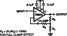
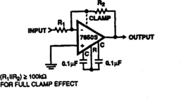
6.4 Output Clamp
Excessive overload recovery time, discussed in Section 5.13.2, is sometimes a problem with chopper-stabilized amplifiers. The problem can be minimized in this IC by the OUTPUT CLAMP circuit. When the OUTPUT CLAMP pin is tied to the inverting (–) input pin, or summing junction, a current path between this point and the OUTPUT pin occurs, just before the IC output saturates. Because of this current path, uncontrolled input differentials are avoided, together with the consequent charge build-up on the correction-storage capacitors. As a result, the output swing is slightly reduced.
6.5 Clock Circuits
The IC has an internal oscillator with a typical chopping frequency of 250 Hz. (This internal clock is available, for external use, at the CLOCK OUT pin on the 14-pin device.) The IC can also be operated by an external clock. The INT/EXT pin has an internal pullup and can be left open for normal operation. To use an external clock, the INT/EXT pin must be tied to V–, thus disabling the internal clock. An external clock signal can then be applied at the EXT CLOCK IN pin.
An internal divide-by-two provides the desired 50% input-switching duty cycle. Because the capacitors are charged only when EXT CLOCK IN is high, a 50% to 80% duty cycle is recommended for the external clock signal. The external clock can swing between V+ and V–. The logic threshold will be at about 2.5 V below V+. Note that a signal of about 400 Hz, with a 70% duty cycle, will be present at the EXT CLOCK IN pin with the INT/EXT high or open. This is the internal clock signal before being fed to the divider.
In those applications where a strobe signal is available, an alternate approach to avoid capacitor misbalancing during overload can be used. If a strobe signal is connected to the EXT CLOCK IN so that the strobe is low during the time that the overload is being applied to the amplifier, neither capacitor will be charged. Because leakage at the capacitor pins is quite low at room temperature, the typical amplifier circuit will drift less than 10 µV/s and relatively long measurements can be made with little change in offset.
6.6 Selecting Capacitors
External capacitors CEXTA and CEXTB have optimum values that depend on the clock or chopping frequency. For the preset internal clock of about 250 Hz, the correct value is 0.1 µF. The value should be scaled approximately in proportion if an external clock is used. This will maintain the same relationship between the chopping frequency and the nulling time constant. A high-quality film-type capacitor such as mylar is recommended, although a ceramic or other lower-grade capacitor may be good for some applications. For the quickest settling after initial turn-on, low-dielectric-absorption capacitors (such as polypropylene) should be used. With ceramic capacitors, several seconds may be required to settle to 1 µV.
6.7 Static Protection
All pins of the IC are static-protected by input diodes (typical for most present-day IC devices). However, strong static fields and discharges should be avoided. Such fields and discharges might result in increased input-leakage currents.
6.8 Avoiding Latchup
Under certain circumstances, the CMOS junction at the IC pins might be triggered into a low-impedance state, resulting in excessive supply current. To avoid this condition, no voltage greater than 0.3 V beyond the supply should be applied to any pin. In general, the amplifier supplies must be established either at the same time or before any input signals are applied. If this is not possible, the circuits driving the inputs must limit input-current flow to under 1 mA to avoid latchup, even under fault conditions.
6.9 Output Load
The output circuit is a high-impedance type (about 18 k). When the output load is less than 18 k, the IC acts somewhat like a transconductance amplifier, where open-loop gain is proportional to load resistance (see Section 4.3). For example, the open-loop gain will be 17 dB lower with an 1-k load than with a 10-k load.
If the IC is used strictly for DC, the lower-gain figure is of little consequence because the DC gain is typically greater than 120 dB, even with a 1-k load. However, for wideband AC applications, the best frequency response will be obtained with a load resistor of 10 k or higher. This results in a smooth 6 dB/octave response from 0.1 Hz to 2 MHz, with phase shifts of less than 10° in the transition region where the main amplifier takes over from the null amplifier.
6.10 Thermoelectric Effects
The ultimate limitations to ultra-high precision DC amplifiers are the thermoelectric or Peltier effects that occur in thermocouple junctions of dissimilar metals, alloys, silicon, etc. Unless all junctions are at the same temperature, thermoelectric voltages (typically about 0.1 µV/°C, but up to tens of mV/°C for some materials) will be generated. This condition requires special precautions to take full advantage of the low offset voltages provided by a chopper-stabilized amplifier. The following is a summary of these precautions.
All components should be enclosed to eliminate air movement, especially that caused by power-dissipating elements in the system. Low thermoelectric-efficient connections should be used where possible. Power supply voltages and power dissipation should be kept to a minimum. High-impedance loads are preferable; good separation from surrounding heat-dissipating elements is advisable.
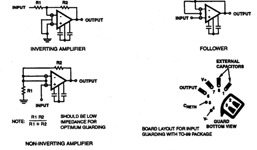
6.11 Guarding
Extra care must be taken in the assembly of PC boards to take full advantage of the low input-currents found in chopper-stabilized amplifiers. Boards must be thoroughly cleaned with TCE or alcohol and blown dry with compressed air. After cleaning, the boards should be coated with epoxy or silicone rubber to prevent contamination.
Even with properly cleaned and coated boards, leakage currents may cause trouble, particularly because the input pins are adjacent to pins at supply potentials. This leakage can be significantly reduced by guarding techniques (to lower the voltage difference between the inputs and adjacent metal runs).
Input guarding of the eight-pin TO-99 package is done with a 10-lead pin circuit, as shown in Fig. 6-3. With this configuration, the holes adjacent to the inputs are empty when the IC is inserted in the board. The guard, which is a conductive ring surrounding the inputs, is connected to a low-impedance point. (The low-impedance point is at approximately the same voltage as the inputs.) Leakage currents from high-voltage pins are then absorbed by the guard.
The pin configuration of the 14-in dual-in-line package (Fig. 6-2) is designed to facilitate guarding. In the 14-pin configuration, the pins adjacent to the inputs are not used. (Note that this is different from the standard 741 and 101A op-amp configuration, but corresponds to that of the LM108.)
6.12 Pin Compatibility
The basic pinout of the 8-pin IC corresponds, where possible, to that of the industry standard eight-pin op-amps (LM741, LM101, etc). The external capacitors are connected to pins 1 and 8, usually used for offset-null or compensation capacitors (or simply not connected for many eight-pin op-amps). In the case of the OP-05 and OP-07 op-amps, the replacement of the offset-null pot (connected between pins 1/8 and V+) can be done by connecting the external capacitors to pins 1 and 8, with the junction or return lead of the capacitors connected to pin 5. This same configuration can be used for replacement of the compensation capacitor used between pins 1 and 8 of an LM108. When the IC is used to replace op-amps such as the LM101 or uA748, the junction between the external capacitors need not be connected to pin 5.
The 14-pin ICL7650S pinout corresponds most closely to that of an LM108 op-amp (because of the NC pins used for guarding between the inputs and other pins). The LM108 does not use any of the extra pins and has no provision for offset-nulling, but does require a compensation capacitor. As a result, some changes in layout are required to use an ICL7650S in place of an LM108.
6.13 Simplified Design of Basic Amplifier Circuits
Figures 6-4 and 6-5 show the basic connections for noninverting and inverting amplifier circuits, respectively, using the ICL7650S. Note that both circuits show a dotted line for the clamp circuits, indicating that the clamp connection is optional. The values of R1, R2, and R3 are not critical, except that the parallel combination of R1 and R2, plus the value of R3, must be greater than 100 k for the noninverting circuit shown in Fig. 6-4. The parallel combination of R1 and R2 must be greater than 100 k for the inverting circuit of Fig. 6-5. The first trial values for the external capacitors should be 0.1 µF, as shown.
6.14 Simplified Design of Booster Circuit
The circuits shown in Figs. 6-4 and 6-5 can be used as replacements for most op-amp circuits, with two limitations. The output-drive capability is limited to a 10-k load to get full output swing and the supply voltage is limited to ±8 V maximum. Both of these limitations can be overcome with a booster circuit such as shown in Fig. 6-6. The circuit of Fig. 6-6 combines the full output capabilities of the 741 (or other standard op-amp) with the low input characteristics of the ICL7650S. However, remember that the two ICs shown form a composite device. As a result, watch the loop-gain stability when a feedback network is added.

6.15 Simplified Design of Low Offset Comparator
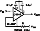
Figure 6-7 shows how the clamp function of an ICL7650S can be used to form a zero-offset comparator. The usual problems in using a chopper-stabilized amplifier as a comparator are avoided. In the Fig. 6-7 circuit, the clamp circuit forces the inverting input to follow the input signal. Note that the threshold input must be capable of tolerating the output-clamp current (approximately equal to VIN/R) without disturbing other portions of the system.
6.16 Combined Chopper/Bipolar Op-Amp
Figure 6-8 shows a circuit that combines the superior DC performance of a dual chopper-stabilized op-amp (the Linear Technology LTC1051) and the ultra low-noise voltage of a precision bipolar op-amp (the Linear Technology LTC1007). Again, as described for the circuit shown in Fig. 6-6, the output characteristics (low noise) are set by the bipolar LTC1007, with the input characteristics set by the LTC1051 (low VOS, VOS drift, input bias current, etc). Although the circuit of Fig. 6-8 can be used wherever stability and low noise are required, the circuit is well suited to such applications as a strain-gauge amplifier. The circuit should be used with source resistances less than 1 k to maintain good noise performance.
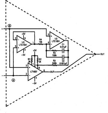
FIGURE 6-8 Combined chopper/bipolar op-amp (Linear Technology, Linear Applications Handbook, 1993, p. DN36–1)
Half of the LTC1051 integrates the LTC1007 input-offset voltage and applies a DC-correction voltage to the LTC1006 at pin 8 through divider R2/R3. The other half of the LTC1051 buffers the VOS-nulling circuits to eliminate loading at input A. Resistors R1, R2, and R3 allow the integrator full output swing, assuring VOS correction to the LTC1007. The ratio of R3 to R2 is made as high as possible to limit noise injection of the chopper into pin 8 of the LTC1007. The total measured input VOS of the combined circuit is 2 µV, with a 10 nV/°C drift.
Figures 6-9 and 6-10 show the recorded peak-to-peak noise of the Fig. 6-8 circuit for a 10-second interval and a 10-minute interval, respectively. During the 10-second interval (Figure 6-9) the peak-to-peak noise is about 100 nV for both the DC-1 Hz and DC-10 Hz bandwidths. During the 10-minute interval (Figure 6-10), the peak-to-peak noise is about 0.2 µV for both the DC-1 Hz and DC-10 Hz bandwidths. This represents a seven to nine times improvement over the DC-10 Hz noise when the LTC1051 is operated alone and tested under the same conditions. The 0.2 µV also represents a 2.5 times improvement over the DC-1 Hz noise of the LTC1051.


6.17 Comparison of Chopper-Stabilized and Bipolar Op-Amps
Figures 6-11 and 6-12 list a number of chopper-stabilized and bipolar op-amps, respectively. Figure 6-13 compares the advantages of the two types of op-amps by listing the parameters of greatest importance. (Note that all the op-amps listed in Figures 6-11 through 6-13 are Linear Technology.) The following is a summary of the comparison.
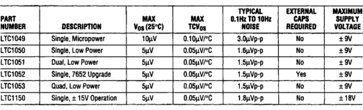
FIGURE 6-11 Typical chopper-stabilized op-amps (Linear Technology, Linear Applications Handbook, 1993, p. DN42–2)
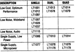
FIGURE 6-12 Precision bipolar op-amps (Linear Technology, Linear Applications Handbook, 1993, p. DN42–2)
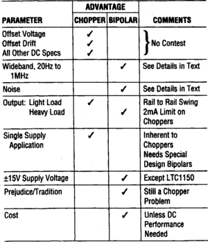
FIGURE 6-13 Comparison of chopper-stabilized and precision bipolar op-amps (Linear Technology, Linear Applications Handbook, 1993, p. DN42–1)
In all input parameters (except noise) the chopper-stabilized op-amps are superior. (A 5 µV maximum offset voltage VOS and a 0.05 µV/°C maximum drift TCVOS are guaranteed for all but the micropower LTC1049.) Changes with time and temperature cycling are near zero. These parameters cannot be measured accurately, but can be guaranteed by design, assuming that the auto-zero chopper loop (which can be tested independently) is working properly. The best tightly specified bipolar op-amps can only approach this performance, at the cost of much testing versus yield expense.
In wideband applications, bipolar op-amps are superior, even though some chopper slew rates are 4 V/µs with bandwidths of 2.5 MHz. However, choppers have clock-frequency spikes, chopping-frequency spikes, aliasing errors, millisecond overload recovery, and high wideband noise.
Where noise performance is critical, bipolar op-amps are again superior. As shown in Fig. 6-14, bipolar noise is nine times better from 10 Hz to 1 kHz. This comparison is for the industry standard LT1001 and the OP-07. Bipolar designs optimized for low noise, such as the LT1007, LT1028, LT1037, or LT1115, have 36 to 100 times lower noise than choppers. However, chopper amplifier noise is flat, whereas bipolar noise depends on frequency (noise increases with decreases in frequency). Therefore, if the bandwidth is limited, chopper noise gets comparatively better.

FIGURE 6-14 Noise comparison of bipolar and chopper-stabilized amplifiers (Linear Technology, Linear Applications Handbook, 1993, p. DN42–1)
Where maximum output swing is required, the bipolar op-amp generally has the edge. Typical chopper-stabilized amplifiers are usually limited to about ±9 V for the power supplies. This in turn limits the output swing to something less than 9 V. An exception is the LTC1150, which operates with standard ± 15-V supplies (typical for most bipolar op-amps). The LTC1150 still guarantees 5-µV offset and the 0.05-µV/°C drift, as shown in Fig. 6-11.