
Pro-Video Composite Interfaces
Digital composite video is essentially a digital version of a composite analog (M) NTSC or (B, D, G, H, I) PAL video signal. The sample clock rate is four times FSC: about 14.32 MHz for (M) NTSC and about 17.73 MHz for (B, D, G, H, I) PAL.
Usually, both 8-bit and 10-bit interfaces are supported, with the 10-bit interface used to transmit 2 bits of fractional video data to minimize cumulative processing errors and to support 10-bit ancillary data.
Table 4.26 lists the digital composite levels. Video data may not use the 10-bit values of 0×000–0×003 and 0×3FC−0×3FF, or the 8-bit values of 0×00 and 0xFF, since they are used for timing information.
Table 4.26. 10-Bit Video Levels for Digital Composite Video Signals
| Video Level | (M) NTSC | (B, D, G, H, I) PAL |
|---|---|---|
| peak chroma | 972 | 1040 (limited to 1023) |
| White | 800 | 844 |
| peak burst | 352 | 380 |
| Black | 280 | 256 |
| Blank | 240 | 256 |
| peak burst | 128 | 128 |
| peak chroma | 104 | 128 |
| Sync | 16 | 4 |
NTSC Video Timing
There are 910 total samples per scan line, as shown in Figure 4.20. Horizontal count 0 corresponds to the start of active video, and a horizontal count of 768 corresponds to the start of horizontal blanking.
Figure 4.20. Digital Composite (M) NTSC Analog and Digital Timing Relationship.

Sampling is along the ±I and ±Q axes (33°, 123°, 213°, and 303°). The sampling phase at horizontal count 0 of line 10, Field 1 is on the +V axis (123°).
The sync edge values, and the horizontal counts at which they occur, are defined as shown in Figure 4.21 and Tables 4.27–4.29. 8-bit values for one color burst cycle are 45, 83, 75, and 37. The burst envelope starts at horizontal count 857, and lasts for 43 clock cycles, as shown in Table 4.27. Note that the peak amplitudes of the burst are not sampled.
Figure 4.21. Digital Composite (M) NTSC Sync Timing. The horizontal counts are shown with the corresponding 8-bit sample values in parentheses.
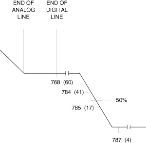
Table 4.27A. Digital Values During the Horizontal Blanking Intervals for Digital Composite (M) NTSC Video Signals
| 8-bit Hex Value | 10-bit Hex Value | |||
|---|---|---|---|---|
| Sample | Fields 1, 3 | Fields 2, 4 | Fields 1, 3 | Fields 2,4 |
| 768–782 | 3C | 3C | 0F0 | 0F0 |
| 783 | 3A | 3A | 0E9 | 0E9 |
| 784 | 29 | 29 | 0A4 | 0A4 |
| 785 | 11 | 11 | 044 | 044 |
| 786 | 04 | 04 | 011 | 011 |
| 787–849 | 04 | 04 | 010 | 010 |
| 850 | 06 | 06 | 017 | 017 |
| 851 | 17 | 17 | 05C | 05C |
| 852 | 2F | 2F | 0BC | 0BC |
| 853 | 3C | 3C | 0EF | 0EF |
| 854–856 | 3C | 3C | 0F0 | 0F0 |
| 857 | 3C | 3C | 0F0 | 0F0 |
| 858 | 3D | 3B | 0F4 | 0EC |
| 859 | 37 | 41 | 0DC | 104 |
| 860 | 36 | 42 | 0D6 | 10A |
| 861 | 4B | 2D | 12C | 0B4 |
| 862 | 49 | 2F | 123 | 0BD |
| 863 | 25 | 53 | 096 | 14A |
| 864 | 2D | 4B | 0B3 | 12D |
| 865 | 53 | 25 | 14E | 092 |
| 866 | 4B | 2D | 12D | 0B3 |
| 867 | 25 | 53 | 092 | 14E |
| 868 | 2D | 4B | 0B3 | 12D |
| 869 | 53 | 25 | 14E | 092 |
| 870 | 4B | 2D | 12D | 0B3 |
| 871 | 25 | 53 | 092 | 14E |
| 872 | 2D | 4B | 0B3 | 12D |
| 873 | 53 | 25 | 14E | 092 |
Table 4.27B. Digital Values During the Horizontal Blanking Intervals for Digital Composite (M) NTSC Video Signals
| 8-bit Hex Value | 10-bit Hex Value | |||
|---|---|---|---|---|
| Sample | Fields 1, 3 | Fields 2, 4 | Fields 1, 3 | Fields 2,4 |
| 874 | 4B | 2D | 12D | 0B3 |
| 875 | 25 | 53 | 092 | 14E |
| 876 | 2D | 4B | 0B3 | 12D |
| 877 | 53 | 25 | 14E | 092 |
| 878 | 4B | 2D | 12D | 0B3 |
| 879 | 25 | 53 | 092 | 14E |
| 880 | 2D | 4B | 0B3 | 12D |
| 881 | 53 | 25 | 14E | 092 |
| 882 | 4B | 2D | 12D | 0B3 |
| 883 | 25 | 53 | 092 | 14E |
| 884 | 2D | 4B | 0B3 | 12D |
| 885 | 53 | 25 | 14E | 092 |
| 886 | 4B | 2D | 12D | 0B3 |
| 887 | 25 | 53 | 092 | 14E |
| 888 | 2D | 4B | 0B3 | 12D |
| 889 | 53 | 25 | 14E | 092 |
| 890 | 4B | 2D | 12D | 0B3 |
| 891 | 25 | 53 | 092 | 14E |
| 892 | 2D | 4B | 0B3 | 12D |
| 893 | 53 | 25 | 14E | 092 |
| 894 | 4A | 2E | 129 | 0B7 |
| 895 | 2A | 4E | 0A6 | 13A |
| 896 | 33 | 45 | 0CD | 113 |
| 897 | 44 | 34 | 112 | 0CE |
| 898 | 3F | 39 | 0FA | 0E6 |
| 899 | 3B | 3D | 0EC | 0F4 |
| 900–909 | 3C | 3C | 0F0 | 0F0 |
Table 4.28. Equalizing Pulse Values During the Vertical Blanking Intervals for Digital Composite (M) NTSC Video Signals
| Fields 1, 3 | Fields 2,4 | ||||
|---|---|---|---|---|---|
| Sample | 8-bit Hex Value | 10-bit Hex Value | Sample | 8-bit Hex Value | 10-bit Hex Value |
| 768–782 | 3C | 0F0 | 313–327 | 3C | 0F0 |
| 783 | 3A | 0E9 | 328 | 3A | 0E9 |
| 784 | 29 | 0A4 | 329 | 29 | 0A4 |
| 785 | 11 | 044 | 330 | 11 | 044 |
| 786 | 04 | 011 | 331 | 04 | 011 |
| 787–815 | 04 | 010 | 332–360 | 04 | 010 |
| 816 | 06 | 017 | 361 | 06 | 017 |
| 817 | 17 | 05C | 362 | 17 | 05C |
| 818 | 2F | 0BC | 363 | 2F | 0BC |
| 819 | 3C | 0EF | 364 | 3C | 0EF |
| 820–327 | 3C | 0F0 | 365–782 | 3C | 0F0 |
| 328 | 3A | 0E9 | 783 | 3A | 0E9 |
| 329 | 29 | 0A4 | 784 | 29 | 0A4 |
| 330 | 11 | 044 | 785 | 11 | 044 |
| 331 | 04 | 011 | 786 | 04 | 011 |
| 332–360 | 04 | 010 | 787–815 | 04 | 010 |
| 361 | 06 | 017 | 816 | 06 | 017 |
| 362 | 17 | 05C | 817 | 17 | 05C |
| 363 | 2F | 0BC | 818 | 2F | 0BC |
| 364 | 3C | 0EF | 819 | 3C | 0EF |
| 365–782 | 3C | 0F0 | 820–327 | 3C | 0F0 |
Table 4.29. Serration Pulse Values During the Vertical Blanking Intervals for Digital Composite (M) NTSC Video Signals
| Fields 1, 3 | Fields 2,4 | ||||
|---|---|---|---|---|---|
| Sample | 8-bit Hex Value | 10-bit Hex Value | Sample | 8-bit Hex Value | 10-bit Hex Value |
| 782 | 3C | 0F0 | 327 | 3C | 0F0 |
| 783 | 3A | 0E9 | 328 | 3A | 0E9 |
| 784 | 29 | 0A4 | 329 | 29 | 0A4 |
| 785 | 11 | 044 | 330 | 11 | 044 |
| 786 | 04 | 011 | 331 | 04 | 011 |
| 787–260 | 04 | 010 | 332–715 | 04 | 010 |
| 261 | 06 | 017 | 716 | 06 | 017 |
| 262 | 17 | 05C | 717 | 17 | 05C |
| 263 | 2F | 0BC | 718 | 2F | 0BC |
| 264 | 3C | 0EF | 719 | 3C | 0EF |
| 265–327 | 3C | 0F0 | 720–782 | 3C | 0F0 |
| 328 | 3A | 0E9 | 783 | 3A | 0E9 |
| 329 | 29 | 0A4 | 784 | 29 | 0A4 |
| 330 | 11 | 044 | 785 | 11 | 044 |
| 331 | 04 | 011 | 786 | 04 | 011 |
| 332–715 | 04 | 010 | 787–260 | 04 | 010 |
| 716 | 06 | 017 | 261 | 06 | 017 |
| 717 | 17 | 05C | 262 | 17 | 05C |
| 718 | 2F | 0BC | 263 | 2F | 0BC |
| 719 | 3C | 0EF | 264 | 3C | 0EF |
| 720–782 | 3C | 0F0 | 265–327 | 3C | 0F0 |
To maintain zero SCH phase, horizontal count 784 occurs 25.6 ns (33° of the subcarrier phase) before the 50% point of the falling edge of horizontal sync, and horizontal count 785 occurs 44.2 ns (57° of the subcarrier phase) after the 50% point of the falling edge of horizontal sync.
PAL Video Timing
There are 1135 total samples per line, except for two lines per frame which have 1137 samples per line, making a total of 709,379 samples per frame. Figure 4.22 illustrates the typical line timing. Horizontal count 0 corresponds to the start of active video, and a horizontal count of 948 corresponds to the start of horizontal blanking.
Figure 4.22. Digital Composite (B, D, G, H, I) PAL Analog and Digital Timing Relationship.

Sampling is along the ±U and ±V axes (0°, 90°, 180°, and 270°), with the sampling phase at horizontal count 0 of line 1, Field 1 on the +V axis (90°).
8-bit color burst values are 95, 64, 32, and 64, continuously repeated. The swinging burst causes the peak burst (32 and 95) and zero burst (64) samples to change places. The burst envelope starts at horizontal count 1058, and lasts for 40 clock cycles.
Sampling is not H-coherent as with (M) NTSC, so the position of the sync pulses changes from line to line. Zero SCH phase is defined when alternate burst samples have a value of 64.
Ancillary Data
Ancillary data packets are used to transmit information (such as digital audio, closed captioning, and teletext data) during the blanking intervals. ITU-R BT.1364 and SMPTE 291M describe the ancillary data formats.
The ancillary data formats are the same as for digital component video, discussed earlier in this chapter. However, instead of a 3-word preamble, a one-word ancillary data flag is used, with a 10-bit value of 3FCH. There may be multiple ancillary data flags following the TRS-ID, with each flag identifying the beginning of another ancillary packet.
Ancillary data may be present within the following word number boundaries (see Figures 4.23 through 4.28).
| NTSC | PAL | |
|---|---|---|
| 795–849 | 972–1035 | horizontal sync period |
| 795–815 | 972–994 | equalizing pulse periods |
| 340–360 | 404–426 | |
| 795–260 | 972–302 | vertical sync periods |
| 340–715 | 404–869 |
Figure 4.23. (M) NTSC TRS-ID and Ancillary Data Locations During Horizontal Sync Intervals.

Figure 4.24. (M) NTSC TRS-ID and Ancillary Data Locations During Vertical Sync Intervals.

Figure 4.25. (M) NTSC TRS-ID and Ancillary Data Locations During Equalizing Pulse Intervals.

Figure 4.26. (B, D, G, H, I) PAL TRS-ID and Ancillary Data Locations During Horizontal Sync Intervals.

Figure 4.27. (B, D, G, H, I) PAL TRS-ID and Ancillary Data Locations During Vertical Sync Intervals.

Figure 4.28. (B, D, G, H, I) PAL TRS-ID and Ancillary Data Locations During Equalizing Pulse Intervals.

User data may not use the 10-bit values of 0×000−0×003 and 0×3FC–0×3FF, or the 8-bit values of 0×00 and 0xFF, since they are used for timing information.
Parallel Interface
The SMPTE 244M 25-pin parallel interface is based on that used for 27 MHz 4:2:2 digital component video (Table 4.24), except for the timing differences. This interface is used to transfer SDTV resolution digital composite data. 8-bit or 10-bit data and a 4×FSC clock are transferred.
Signal levels are compatible with ECL-compatible balanced drivers and receivers. The generator must have a balanced output with a maximum source impedance of 110 Ω; the signal must be 0.8–2.0 V peak-to-peak measured across a 110 Ω load. At the receiver, the transmission line must be terminated by 110±10 Ω.
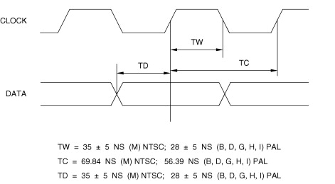
The clock signal is a 4×FSC square wave, with a clock pulse width of 35 ±5 ns for (M) NTSC or 28 ±5 ns for (B, D, G, H, I) PAL. The positive transition of the clock signal occurs midway between data transitions with a tolerance of ±5 ns (as shown in Figure 4.29).
Figure 4.29. Digital Composite Video Parallel Interface Waveforms.
To permit reliable operation at interconnect lengths of 50–200 meters, the receiver must use frequency equalization, with typical characteristics shown in Figure 4.14. This example enables operation with a range of cable lengths down to zero.
Serial Interface
The parallel format can be converted to a SMPTE 259M serial format (Figure 4.30), allowing data to be transmitted using a coaxial cable (or optical fiber). This interface converts the 14.32 or 17.73 MHz parallel stream into a 143 or 177 Mbps serial stream. The 10× PLL generates the 143 or 177 MHz clock from the 14.32 or 17.73 MHz clock signal.
Figure 4.30. Serial Interface Block Diagram.

For cable interconnect, the generator has an unbalanced output with a source impedance of 75 ?; the signal must be 0.8 V ±10% peak-to-peak measured across a 75 Ω load. The receiver has an input impedance of 75 Ω.
How It Works
The 10 bits of data are serialized (LSB first) and processed using a scrambled and polarity-free NRZI algorithm:
This algorithm is the same as used for digital component video discussed earlier. In an 8-bit environment, 8-bit data is appended with two least significant “0” bits before serialization.
The input signal to the scrambler (Figure 4.18) uses positive logic (the highest voltage represents a logical one; lowest voltage represents a logical zero). The formatted serial data is output at the 40×FSC rate.
At the receiver, phase-lock synchronization is done by detecting the TRS-ID sequences. The PLL is continuously adjusted slightly each scan line to ensure that these patterns are detected and to avoid bit slippage. The recovered 10×clock is divided by ten to generate the 4×FSC sample clock. The serial data is low- and high-frequency equalized, inverse scrambling performed (Figure 4.19), and deserialized.