
Parallel Interfaces
25-pin Parallel interface
This interface is used to transfer SDTV resolution 4:2:2 YCbCr data. 8-bit or 10-bit data and a clock are transferred. The individual bits are labeled D0–D9, with D9 being the most significant bit. The pin allocations for the signals are shown in Table 4.24.
Figure 4.12. BT.656 Parallel Interface Data For One Scan Line. 480i; 4:2:2 YCbCr; 720 active samples per line; 27 MHz clock; 10-bit system. The values for 576i systems are shown in parentheses.
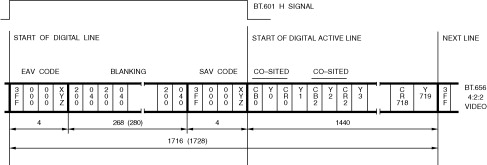
Table 4.24. 25-Pin Parallel Interface Connector Pin Assignments. For 8-bit interfaces, D9–D2 are used
| Pin | Signal | Pin | Signal |
|---|---|---|---|
| 1 | clock | 14 | clock− |
| 2 | system ground A | 15 | system ground B |
| 3 | D9 | 16 | D9− |
| 4 | D8 | 17 | D8− |
| 5 | D7 | 18 | D7− |
| 6 | D6 | 19 | D6− |
| 7 | D5 | 20 | D5− |
| 8 | D4 | 21 | D4− |
| 9 | D3 | 22 | D3− |
| 10 | D2 | 23 | D2− |
| 11 | D1 | 24 | D1− |
| 12 | D0 | 25 | D0− |
| 13 | cable shield |
Y has a nominal 10-bit range of 0×040–0×3AC. Values less than 0×040 or greater than 0×3AC may be present due to processing. During blanking, Y data should have a value of 040H, unless other information is present.
Cb and Cr have a nominal 10-bit range of 0×040–0×3C0. Values less than 0×040 or greater than 0×3C0 may be present due to processing. During blanking, CbCr data should have a value of 0×200, unless other data is present.
Signal levels are compatible with ECL-compatible balanced drivers and receivers. The generator must have a balanced output with a maximum source impedance of 110?; the signal must be 0.8–2.0 V peak-to-peak measured across a 110-? load. At the receiver, the transmission line is terminated by 110±10?
27 MHz Parallel Interface: This BT.656 and SMPTE 125M interface is used for 480i and 576i systems with an aspect ratio of 4:3. Y and multiplexed CbCr information at a sample rate of 13.5 MHz are multiplexed into a single 8-bit or 10-bit data stream, at a clock rate of 27 MHz.
The 27 MHz clock signal has a clock pulse width of 18.5±3 ns. The positive transition of the clock signal occurs midway between data transitions with a tolerance of ±3 ns (as shown in Figure 4.13).
Figure 4.13. 25-Pin 27 MHz Parallel Interface Waveforms.

To permit reliable operation at interconnect lengths of 50–200 meters, the receiver must use frequency equalization, with typical characteristics shown in Figure 4.14. This example enables operation with a range of cable lengths down to zero.
Figure 4.14. Example Line Receiver Equalization Characteristics for Small Signals.

36 MHz Parallel Interface: This BT.1302 and SMPTE 267M interface is used for 480i and 576i systems with an aspect ratio of 16:9. Y and multiplexed CbCr information at a sample rate of 18 MHz are multiplexed into a single 8-bit or 10-bit data stream, at a clock rate of 36 MHz.
The 36 MHz clock signal has a clock pulse width of 13.9±2 ns. The positive transition of the clock signal occurs midway between data transitions with a tolerance of ±2 ns (as shown in Figure 4.15).
Figure 4.15. 25-Pin 36 MHz Parallel Interface Waveforms.

To permit reliable operation at interconnect lengths of 40–160 meters, the receiver must use frequency equalization, with typical characteristics shown in Figure 4.14.
93-pin Parallel interface
This interface is used to transfer HDTV resolution R′G′B′ data, 4:2:2 YCbCr data, or 4:2:2:4 YCbCrK data. The pin allocations for the signals are shown in Table 4.25. The most significant bits are R9, G9, and B9.
Table 4.25. 93-Pin Parallel Interface Connector Pin Assignments. For 8-bit interfaces, bits 9–2 are used
| Pin | Signal | Pin | Signal | Pin | Signal | Pin | Signal |
|---|---|---|---|---|---|---|---|
| 1 | clock | 26 | GND | 51 | B2 | 76 | GND |
| 2 | G9 | 27 | GND | 52 | B1 | 77 | GND |
| 3 | G8 | 28 | GND | 53 | B0 | 78 | GND |
| 4 | G7 | 29 | GND | 54 | R9 | 79 | B4− |
| 5 | G6 | 30 | GND | 55 | R8 | 80 | B3− |
| 6 | G5 | 31 | GND | 56 | R7 | 81 | B2− |
| 7 | G4 | 32 | GND | 57 | R6 | 82 | B1− |
| 8 | G3 | 33 | clock− | 58 | R5 | 83 | B0− |
| 9 | G2 | 34 | G9− | 59 | R4 | 84 | R9− |
| 10 | G1 | 35 | G8− | 60 | R3 | 85 | R8− |
| 11 | G0 | 36 | G7− | 61 | R2 | 86 | R7− |
| 12 | B9 | 37 | G6− | 62 | R1 | 87 | R6− |
| 13 | B8 | 38 | G5− | 63 | R0 | 88 | R5− |
| 14 | B7 | 39 | G4− | 64 | GND | 89 | R4− |
| 15 | B6 | 40 | G3− | 65 | GND | 90 | R3− |
| 16 | B5 | 41 | G2− | 66 | GND | 91 | R2− |
| 17 | GND | 42 | G1− | 67 | GND | 92 | R1− |
| 18 | GND | 43 | G0− | 68 | GND | 93 | R0− |
| 19 | GND | 44 | B9− | 69 | GND | ||
| 20 | GND | 45 | B8− | 70 | GND | ||
| 21 | GND | 46 | B7− | 71 | GND | ||
| 22 | GND | 47 | B6− | 72 | GND | ||
| 23 | GND | 48 | B5− | 73 | GND | ||
| 24 | GND | 49 | B4 | 74 | GND | ||
| 25 | GND | 50 | B3 | 75 | GND |
When transferring 4:2:2 YCbCr data, the green channel carries Y information and the red channel carries multiplexed CbCr information.
When transferring 4:2:2:4 YCbCrK data, the green channel carries Y information, the red channel carries multiplexed CbCr information, and the blue channel carries K (alpha keying) information.
Y has a nominal 10-bit range of 0×040−0×3AC. Values less than 040H or greater than 0×3AC may be present due to processing. During blanking, Y data should have a value of 0×040, unless other information is present.
Cb and Cr have a nominal 10-bit range of 0×040–0×3C0. Values less than 0×040 or greater than 0×3C0 may be present due to processing. During blanking, CbCr data should have a value of 0×200, unless other information is present.
R′G′B′ and K have a nominal 10-bit range of 0×040–0×3AC. Values less than 0×040 or greater than 0×3AC may be present due to processing. During blanking, R′G′B′ data should have a value of 0×040, unless other information is present.
Signal levels are compatible with ECL-compatible balanced drivers and receivers. The generator must have a balanced output with a maximum source impedance of 110Ω; the signal must be 0.6–2.0 V peak-to-peak measured across a 110Ω load. At the receiver, the transmission line must be terminated by 110±10.
74.25 and 74.176 MHz Parallel Interface: This ITU-R BT.1120 and SMPTE 274M interface is primarily used for HDTV systems. The 74.25 or 74.176 MHz (74.25/1.001) clock signal has a clock pulse width of 6.73±1.48 ns. The positive transition of the clock signal occurs midway between data transitions with a tolerance of ±1 ns (as shown in Figure 4.16).
Figure 4.16. 93-Pin 74.25 and 74.176 MHz Parallel Interface Waveforms.

To permit reliable operation at interconnect lengths greater than 20 meters, the receiver must use frequency equalization.
148.5 and 148.35 MHz Parallel Interface: This BT.1120 and SMPTE 274M interface is used for HDTV systems. The 148.5 or 148.35 MHz (148.5/1.001) clock signal has a clock pulse width of 3.37±0.74 ns. The positive transition of the clock signal occurs midway between data transitions with a tolerance of ±0.5 ns (similar to Figure 4.16). To permit reliable operation at interconnect lengths greater than 14 meters, the receiver must use frequency equalization.
Serial Interfaces
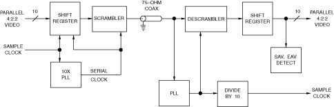
The parallel formats can be converted to a serial format (Figure 4.17), allowing data to be transmitted using a 75 Ω coaxial cable or optical fiber.
Figure 4.17. Serial Interface Block Diagram.
For cable interconnect, the generator has an unbalanced output with a source impedance of 75 Ω; the signal must be 0.8 V ±10% peak-to-peak measured across a 75 Ω load. The receiver has an input impedance of 75 Ω.
How It Works
In an 8-bit environment, before serialization, the 0×00 and 0xFF codes during EAV and SAV are expanded to 10-bit values of 0×000 and 0×3FF, respectively. All other 8-bit data is appended with two least significant “0” bits before serialization.
The 10 bits of data are serialized (LSB first) and processed using a scrambled and polarity-free NRZI algorithm:
The input signal to the scrambler (Figure 4.18) uses positive logic (the highest voltage represents a logical one; lowest voltage represents a logical zero). The formatted serial data is output at the 10×sample clock rate. Since the parallel clock may contain large amounts of jitter, deriving the 10×sample clock directly from an unfiltered parallel clock may result in excessive signal jitter.
Figure 4.18. Typical Scrambler Circuit.

At the receiver, phase-lock synchronization is done by detecting the EAV and SAV sequences. The PLL is continuously adjusted slightly each scan line to ensure that these patterns are detected and to avoid bit slippage. The recovered 10× sample clock is divided by ten to generate the sample clock, although care must be taken not to mask word-related jitter components. The serial data is low- and high-frequency equalized, inverse scrambling performed (Figure 4.19), and deserialized.
Figure 4.19. Typical Descrambler Circuit.
