CHAPTER 1 The Op Amp
Chapter Introduction
In this chapter we will discuss the basic operation of the op amp, one of the most common linear design building blocks.
In Section 1-1 the basic operation of the op amp will be discussed. We will concentrate on the op amp from the black box point of view. There are a good many texts that describe the internal workings of an op amp, so in this work a more macro view will be taken. There are a couple of times, however, that we will talk about the insides of the op amp. It is unavoidable.
In Section 1-2 the basic specifications will be discussed. Some techniques to compensate for some of the op amps limitations will also be given.
Section 1-3 will discuss how to read a data sheet. The various sections of the data sheet and how to interpret what is written will be discussed.
Section 1-4 will discuss how to select an op amp for a given application.
SECTION 1-1 Op Amp Operation
Introduction
The op amp is one of the basic building blocks of linear design. In its classic form it consists of two input terminals—one of which inverts the phase of the signal, the other preserves the phase—and an output terminal. The standard symbol for the op amp is given in Figure 1-1. This ignores the power supply terminals, which are obviously required for operation.

The name “op amp” is the standard abbreviation for operational amplifier. This name comes from the early days of amplifier design, when the op amp was used in analog computers. (Yes, the first computers were analog in nature, rather than digital.) When the basic amplifier was used with a few external components, various mathematical “operations” could be performed. One of the primary uses of analog computers was during World War II, when they were used for plotting ordinance trajectories.
Voltage Feedback Model
The classic model of the voltage feedback (VFB) op amp incorporates the following characteristics:
None of these can be actually realized, of course. How close we come to these ideals determines the quality of the op amp.
This is referred to as the VFB model. This type of op amp comprises nearly all op amps below 10 MHz bandwidth and on the order of 90% of those with higher bandwidths (Figure 1-2).

Basic Operation
The basic operation of the op amp can be easily summarized. First we assume that there is a portion of the output that is feedback to the inverting terminal to establish the fixed gain for the amplifier. This is negative feedback. Any differential voltage across the input terminals of the op amp is multiplied by the amplifier’s open-loop gain. If the magnitude of this differential voltage is more positive on the inverting (−) terminal than on the non-inverting (+) terminal, the output will go more negative. If the magnitude of the differential voltage is more positive on the non-inverting (+) terminal than on the inverting (−) terminal, the output voltage will become more positive. The open-loop gain of the amplifier will attempt to force the differential voltage to zero. As long as the inouts and output stays in the operational range of the amplifier, it will keep the differential voltage at zero and the output will be the input voltage multiplied by the gain set by the feedback. Note from this that the inputs respond to differential-mode not common-mode input voltage:
Inverting and Non-Inverting Configurations
There are two basic ways configure the VFB op amp as an amplifier. These are shown in Figure 1-3 and Figure 1-4.


Figure 1-3 shows what is known as the inverting configuration. With this circuit, the output is out of phase with the input. The gain of this circuit is determined by the ratio of the resistors used and is given by:
Figure 1-4 shows what is know as the non-inverting configuration. With this circuit, the output is in phase with the input. The gain of the circuit is also determined by the ratio of the resistors used and is given by:
Note that since the output drives a voltage divider (the gain setting network) the maximum voltage available at the inverting terminal is the full output voltage, which yields a minimum gain of 1.
Also note that in both cases the feedback is from the output to the inverting terminal. This is negative feedback and has many advantages for the designer. These will be discussed in more detail further in this chapter.
It should also be noted that the gain is based on the ratio of the resistors, not their actual values. This means that the designer can choose just about any value he or she wishes within practical limits.
If the value of the resistors is too low, a great deal of current would be required from the op amps output for operation. This causes excessive dissipation in the op amp itself, which has many disadvantages. The increased dissipation leads to self-heating of the chip, which could cause a change in the DC characteristics of the op amp itself. Also the heat generated by the dissipation could eventually cause the junction temperature to rise above the 150°C, the commonly accepted maximum limit for most semiconductors.
The junction temperature is the temperature at the silicon chip itself. On the other end of the spectrum, if the resistor values are too high, there is an increase in noise and the susceptibility to parasitic capacitances, which could also limit bandwidth and possibly cause instability and oscillation.
From a practical sense, resistors below 10 Ω and above 1 MΩ become increasingly difficult to purchase especially if precision resistors are required.
Let us look at the case of an inverting amp in a little more detail. Referring to Figure 1-5, the non-inverting terminal is connected to ground. (We are assuming a bipolar (+ and −) power supply.) Since the op amp will force the differential voltage across the inputs to zero, the inverting input will also appear to be at ground. In fact, this node is often referred to as a “virtual ground.”
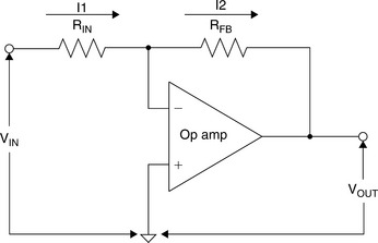
If there is a voltage (VIN) applied to the input resistor, it will set up a current (I1) through the resistor (RIN) so that:
Since the input impedance of the op amp is infinite, no current will flow into the inverting input. Therefore, this same current (I1) must flow through the feedback resistor (RFB). Since the amplifier will force the inverting terminal to ground, the output will assume a voltage (VOUT) such that:
Doing a little simple arithmetic we then can come to the conclusion of Eq. (1-1):
Now we examine the non-inverting case in more detail. Referring to Figure 1-6, the input voltage is applied to the non-inverting terminal. The output voltage drives a voltage divider consisting of RFB and RIN. The name “RIN,” in this instance, is somewhat misleading since the resistor is not technically connected to the input, but we keep the same designation since it matches the inverting configuration, has become a de facto standard, anyway. The voltage at the inverting terminal (Va), which is at the junction of the two resistors, is:
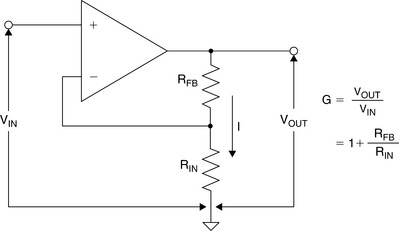
The negative feedback action of the op amp will force the differential voltage to 0 so:
Again applying a little simple arithmetic we end up with:
Which is what we specified in Eq. (1-2).
In all of the discussions above, we referred to the gain setting components as resistors. In fact, they are impedances, not just resistances. This allows us to build frequency dependent amplifiers. This will be covered in more detail in a later section.
Open-Loop Gain
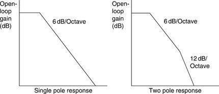
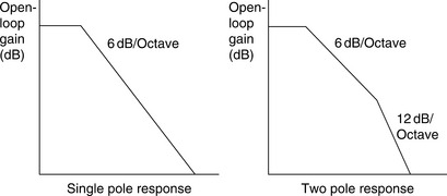
The open-loop gain (usually referred to as AVOL) is the gain of the amplifier without the feedback loop being closed, hence the name “open loop.” For a precision op amp this gain can be vary high, on the order of 160 dB or more. This is a gain of 100 million. This gain is flat from DC to what is referred to as the dominant pole. From there it falls off at 6 dB/octave or 20 dB/decade. (An octave is a doubling in frequency and a decade is × 10 in frequency.) This is referred to as a single pole response. It will continue to fall at this rate until it hits another pole in the response. This second pole will double the rate at which the open-loop gain falls, i.e., to 12 dB/octave or 40 dB/decade. If the open-loop gain has dropped below 0 dB (unity gain) before it hits the second pole, the op amp will be unconditionally stable at any gain. This will be typically referred to as unity gain stable on the data sheet. If the second pole is reached while the loop gain is greater than 1 (0 dB), then the amplifier may not be stable under some conditions (Figure 1-7).
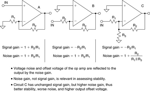
It is important to understand the differences between open-loop gain, closed-loop gain, loop gain, signal gain, and noise gain (Figures 1-8 and 1-9). They are similar in nature, interrelated, but different. We will discuss them all in detail.

The open-loop gain is not a precisely controlled specification. It can, and does, have a relatively large range and will be given in the specifications as a typical number rather than a min/max number, in most cases. In some cases, typically high precision op amps, the specification will be a minimum.
In addition, the open-loop gain can change due to output voltage levels and loading. There is also some dependency on temperature. In general, these effects are of a very minor degree and can, in most cases, be ignored. In fact this nonlinearity is not always included in the data sheet for the part.
Gain-Bandwidth Product
The open-loop gain falls at 6 dB/octave. This means that if we double the frequency, the gain falls to half of what it was. Conversely, if the frequency is halved, the open-loop gain will double, as shown in Figure 1-8. This gives rise to what is known as the Gain-Bandwidth Product. If we multiply the open-loop gain by the frequency, the product is always a constant. The caveat for this is that we have to be in the part of the curve that is falling at 6 dB/octave. This gives us a convenient figure of merit with which to determine if a particular op amp is useable in a particular application (Figure 1-10).

For example, if we have an application with which we require a gain of 10 and a bandwidth of 100 kHz, we require an op amp with, at least, a gain-bandwidth product of 1 MHz. This is a slight oversimplification. Because of the variability of the gain-bandwidth product, and the fact that at the location where the closed-loop gain intersects the open-loop gain the response is actually down 3 dB, a little margin should be included. In the application described above, an op amp with a gain-bandwidth product of 1 MHz would be marginal. A safety factor of at least 5 would be better insurance that the expected performance is achieved.
Stability Criteria
Feedback theory states that the closed-loop gain must intersect the open-loop gain at a rate of 6 dB/octave (single pole response) for the system to be stable. If the response is 12 dB/octave (two pole response) the op amp will oscillate. The easiest way to think of this is that each pole adds 90° of phase shift. Two poles then means 180°, and 180° of phase shift turns negative feedback into positive feedback, which means oscillations.
The question could be then, why would you want an amplifier that is not unity gain stable. The answer is that for a given amplifier, the bandwidth can be increased if the amplifier is not unity gain stable. This is sometimes referred to as decompensated, but the gain criteria must be met. This criteria is that the closed-loop gain must intercept the open-loop gain at a slope of 6 dB/octave (single pole response). If not, the amplifier will oscillate.
As an example, compare the open-loop gain graphs in Figures 1-11, 1-12, 1-13. The three parts shown, the AD847, AD848, and AD849, are basically the same part. The AD847 is unity gain stable. The AD848 is stable for gains of two or more. The AD849 is stable for a gain of 10 or more.

Phase Margin
One measure of stability is phase margin. Just as the amplitude response does not stay flat and then change instantaneously, the phase will also change gradually, starting as much as a decade back from the corner frequency. Phase margin is the amount of phase shift that is left until you hit 180° measured at the unity gain point.
The manifestation of low phase margin is an increase in the peaking of the output just before the close loop gain intersects the open-loop gain (see Figure 1-14).

Closed-Loop Gain
This, of course, is the gain of the amplifier with the feedback loop closed, as opposed the open-loop gain, which is the gain with the feedback loop opened. It has two forms, signal gain and noise gain. These are described and differentiated below.
The expression for the gain of a closed-loop amplifier involves the open-loop gain. If G is the actual gain, NG is the noise gain (see below), and AVOL is the open-loop gain of the amplifier, then:
 (1-9)
(1-9)From this you can see that if the open-loop gain is very high, which it typically is, the closed-loop gain of the circuit is simply the noise gain.
Signal Gain
This is the gain applied to the input signal, with the feedback loop connected. In the basic operation section above, when we talked about the gain of the inverting and non-inverting circuits, we were actually more correctly talking about the closed-loop signal gain. It can be inverting or non-inverting. It can even be less than unity for the inverting case. Signal gain is the gain that we are primarily interested in when designing circuits.
The signal gain for an inverting amplifier stage is:
and for a non-inverting amplifier it is:
Noise Gain
Noise gain is the gain applied to a noise source in series with an op amp input. It is also the gain applied to an offset voltage. The noise gain is equal to:
Noise gain is equal to the signal gain of a non-inverting amp. It is the same for either an inverting or non-inverting stage.
It is the noise gain that is used to determine stability. It is also the closed-loop gain that is used in Bode plots. Remember that even though we used resistances in the equation for noise gain, they are actually impedances (see Figure 1-9).
Loop Gain
The difference between the open- and the closed-loop gain is known as the loop gain. This is useful information because it gives you the amount of negative feedback that can apply to the amplifier system (see Figure 1-8).
Bode Plot
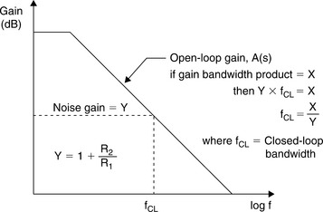
The plotting of open-loop gain versus frequency on a log–log scale gives is what is known as a Bode (pronounced boh dee) plot. It is one of the primary tools in evaluating whether a particular op amp is suitable for a particular application.
If you plot the open-loop gain and then the noise gain on a Bode plot, the point where they intersect will determine the maximum closed-loop bandwidth of the amplifier system. This is commonly referred to as the closed-loop frequency (FCL). Remember that the true response at the intersection is actually 3 dB down. One octave above and one octave below FCL, the difference between the asymptotic response and the real response will be less than 1 dB (Figure 1-15).

The Bode plot is also useful in determining stability. As stated above, if the closed-loop gain (noise gain) intersects the open-loop gain at a slope of greater than 6 dB/octave (20 dB/decade), the amplifier may be unstable (depending on the phase margin).
Current Feedback Model
There is a type of amplifiers that have several advantages over the standard VFB amplifier at high frequencies. They are called current feedback (CFB) or sometimes transimpedance amps. There is a possible point of confusion since the current-to-voltage (I/V) converters commonly found in photodiode applications are also referred to as transimpedance amps. Schematically CFB op amps look similar to standard VFB amps, but there are several key differences.
The input structure of the CFB is different from the VFB. While we are trying not to get into the internal structures of the op amps, in this case a simple diagram is in order (see Figure 1-16). The mechanism of feedback is also different, hence the names. But again, the exact mechanism is beyond what we want to cover here. In most cases if the differences are noted, and the attendant limitations observed, the basic operation of both types of amplifiers can be thought of as the same. The gain equations are the same as for a VFB amp, with an important limitation as noted in the next section.

Difference from VFB
One primary difference between the CFB and VFB amps is that there is not a gain-bandwidth product. While there is a change in bandwidth with gain, it is not even close to the 6 dB/octave that we see with VFB (see Figure 1-17). Also, a major limitation is that the value of the feedback resistor determines the bandwidth, working with the internal capacitance of the op amp. For every CFB op amp there is a recommended value of feedback resistor for maximum bandwidth. If you increase the value of the resistor, reduce the bandwidth. If you use a lower value of resistor, the phase margin is reduced and the amplifier could become unstable. This optimum value of resistor is different for different operational conditions. For instance, the value will change for different packages, e.g., SOIC versus DIP (see Figure 1-18).


Also, a CFB amplifier should not have a capacitor in the feedback loop. If a capacitor is used in the feedback loop, it reduces the feedback impedance as frequency is increased, which will cause the op amp to oscillate. You need to be careful of stray capacitances around the inverting input of the op amp for the same reason.
A common error in using a CFB op amp is to short the inverting input directly to the output in an attempt to build a unity gain voltage follower (buffer). This circuit will oscillate. Obviously, in this case, the feedback resistor value will be less than the recommended value. The circuit is perfectly stable if the recommended feedback resistor of the correct value is used in place of the short.
Another difference between the VFB and CFB amplifiers is that the inverting input of the CFB amp is low impedance. By low we mean typically 50–100 Ω. Therefore, there is not the inherent balance between the inputs that the VFB circuit shows.
Slew-rate performance is also enhanced by the CFB topology. The current that is available to charge the internal compensation capacitor is dynamic. It is not limited to any fixed value as is often the case in VFB topologies. With a step input or overload condition, the current is increased (current-on-demand) until the overdriven condition is removed. The basic CFB amplifier has no fundamental slew-rate limit. Limits only come about from parasitic internal capacitances and many strides have been made to reduce their effects.
The combination of higher bandwidths and slew rate allows CFB devices to have good distortion performance while doing so at a lower power.
The distortion of an amplifier is impacted by the open-loop distortion of the amplifier and the loop gain of the closed-loop circuit. The amount of open-loop distortion contributed by a CFB amplifier is small due to the basic symmetry of the internal topology. Speed is the other main contributor to distortion. In most configurations, a CFB amplifier has a greater bandwidth than its VFB counterpart. So at a given signal frequency, the faster part has greater loop gain and therefore lower distortion.
How to Choose Between CFB and VFB
The application advantages of CFB and VFB differ. In many applications, the differences between CFB and VFB are not readily apparent. Today’s CFB and VFB amplifiers have comparable performance, but there are certain unique advantages associated with each topology. VFB allows freedom of choice of the feedback resistor (or impedance) at the expense of sacrificing bandwidth for gain. CFB maintains high bandwidth over a wide range of gains at the cost of limiting the choices in the feedback impedance.
while CFB amplifiers offer:Supply Voltages
Historically the supply voltage for op amps was typically ± 15 V. The operational input and output range was on the order of ± 10 V. But there was no hard requirement for these levels. Typically the maximum supply was ± 18 V. The lower limit was set by the internal structures. You could typically go within 1.5 or 2 V of either supply rail, so you could reasonably go down to ±8 V supplies or so and still have a reasonable dynamic range.
Lately though, there has been a trend toward lower supply voltages. This has happened for a couple of reasons.
First, high speed circuits typically have a lower full-scale range. The principal reason for this is the amplifier’s ability to swing large voltages. All amplifiers have a slew-rate limit, which is expressed as so many volts per microsecond. So if you want to go faster, your voltage range must be reduced, all other things being equal. Another reason is that to limit the effects of stray capacitance on the circuits, you need to reduce their impedance levels. Driving lower impedances increases the demands on the output stage, and on the power dissipation abilities of the amplifier package. Lower voltage swings require lower currents to be supplied, thereby lowering the dissipation of the package.
A second reason is that as the speed of the devices inside the amplifier increased, the geometries of these devices tend to become smaller. The smaller geometries typically mean reduced breakdown voltages for these parts. Since the breakdown voltages were getting lower, the supply voltages had to follow. Today high speed op amps typically have breakdown voltage of ±7 V, and so the supplies are typically ±5 V, or even lower.
In some cases, operation on batteries established a requirement for lower supply voltages. Lower supplies would then lessen the number of batteries, which, in turn, reduced the size, weight, and cost of the end product.
At the same time there was a movement towards single supply systems. Instead of the typical plus and minus supplies, the op amps operate on a single positive supply and ground, the ground then becoming the negative supply.
Single Supply Considerations
There is nothing in the circuitry of the op amp that requires ground. In fact, instead of a bipolar (+ and −) supply of ± 15 V you could just as easily use a single supply of + 30 V (ground being the negative supply), as long as the rest of the circuit was biased correctly so that the signal was within the common-mode range of op amp. Or, for that matter, the supply could just as easily be −30 V (ground being the most positive supply).
When you combine the single supply operation with reduced supply voltages, you can run into problems. The standard topology for op amps uses a NPN differential pair (see Figure 1-19) for the input and emitter followers (see Figure 1-22) for the output stage. Neither of these circuits will let you run “rail-to-rail,” i.e., from one supply to the other. Some circuit modifications are required.
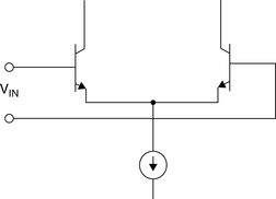

Figure 1-22: Output stages: Emitter follower for standard configuration and common emitter for “rail-to-rail” configuration
The first of these modifications was the use of a PNP differential input (see Figure 1-20). One of the first examples of this input configuration was the LM324. This configuration allowed the input to get close to the negative rail (ground). It could not, however, go to the positive rail, But in many systems, especially mixed signal systems that were predominately digital, this was enough. In terms of precision, the 324 is not a stellar performer.
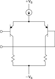
The NPN input cannot swing to ground. The PNP input cannot swing to the positive rail. The next modification was to use a dual input. Here a NPN differential pair is combined with a PNP differential pair (see Figure 1-21). Over most of the common-mode range of the input both pairs are active. As one rail or the other is approached, one of the inputs turns off. The NPN pair swings to the upper rail and the PNP pair swings to the lower rail.

It should be noted here that the op amp parameters which primarily depend on the input structure (bias current, for instance) will vary with the common-mode voltage on the inputs. The bias currents will even change direction as the front end transitions from the NPN stage to the PNP stage.
Another difference is the output stage. The standard output stage, which is a complimentary emitter follower (common collector) configuration, is typically replaced by a common emitter circuit (Figure 1-22). This allows the output to swing close to the rails. The exact level is set by the VCEsat of the output transistors, which is, in turn, dependent on the output current levels. The only real disadvantage to this arrangement is that the output impedance of the common emitter circuit is higher than the common collector circuit. Most of the time this is not really an issue, since negative feedback reduces the output impedance proportional to the amount of loop gain. Where it becomes an issue is that as the loop gain falls this higher output impedance is more susceptible to the effects of capacitive loading.
Circuit Design Considerations for Single Supply Systems
Many waveforms are bipolar in nature. This means that the signal naturally swings around the reference level, which is typically ground. This obviously will not work in a single supply environment. What is required is to AC couple the signals.
AC coupling is simply applying a high pass filter and establishing a new reference level typically somewhere around the center of the supply voltage range (see Figure 1-23). The series capacitor will block the DC component of the input signal. The corner frequency (the frequency at which the response is 3 dB down from the midband level) is determined by the value of the components:

where:
It should be noted that if multiple sections are AC coupled, each section will be 3 dB down at the corner frequency. So if there are two sections with the same corner frequency, the total response will be 6 dB down; three sections would be 9 dB down, etc. This should be taken into account so that the overall response of the system will be adequate. Also keep in mind that the amplitude response starts to roll off a decade, or more, from the corner frequency.
The AC coupling of arbitrary waveforms can actually introduce problems which do not exist at all in DC coupled systems. These problems have to do with the waveform duty cycle, and are particularly acute with signals which approach the rails, as they can in low supply voltage systems which are AC coupled.
In an amplifier circuit such as that of Figure 1-23, the output bias point will be equal to the DC bias as applied to the op amp’s (+) input. For a symmetric (50% duty cycle) waveform of a 2 Vp-p output level, the output signal will swing symmetrically about the bias point, or nominally 2.5 ± 1 V (using the values give in Figure 1-23). If however the pulsed waveform is of a very high (or low) duty cycle, the AC averaging effect of CIN and R4 ‖ R5 will shift the effective peak level either high or low, dependent on the duty cycle. This phenomenon has the net effect of reducing the working headroom of the amplifier, and is illustrated in Figure 1-24.
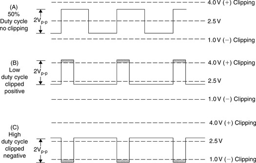
In Figure 1-24(A), an example of a 50% duty cycle square wave of about 2 Vp-p level is shown, with the signal swing biased symmetrically between the upper and lower clip points of a 5 V supply amplifier. This amplifier, for example, (an AD817 biased similarly to Figure 1-23) can only swing to the limited DC levels as marked, about 1 V from either rail. In cases (B) and (C), the duty cycle of the input waveform is adjusted to both low and high duty cycle extremes while maintaining the same peak-to-peak input level. At the amplifier output, the waveform is seen to clip either negative or positive, in (B) and (C), respectively.
Rail-to-Rail
When the input and/or the output can swing very close to the supply rails, it is referred to as “rail-to-rail.” There is no industry standard definition for this. At Analog Devices (ADI) we have defined this at swinging to within 100 mV of either rail. For the output this is driving a standard load, since the actual maximum output level will depend on the output current. Note that not all amplifiers that are touted as single supply are rail-to-rail. And not all rail-to-rail amplifiers are rail-to-rail on input and output. It could be one or the other, both, or neither. The bottom line is that you must read the data sheet. In no case can the output actually swing completely to the rails.
Phase Reversal
There is an interesting phenomenon that can occur when the common-mode range of the op amp is exceeded. Some internal nodes can turn off and the output will be pulled to the opposite rail until the input comes back into the operational range (see Figure 1-25). Many modern designs take steps to eliminate this problem. Many times this is called out in the bullets on the cover page. Phase reversal is most common when the amplifier is in the follower mode.

Low Power and Micropower
Along with the trend toward single supplies is the trend toward lower quiescent power. This is the power used by the amp itself. We have arrived at the point where there are whole amplifiers that can operate on the bias current of the 741.
However, low power involves some tradeoffs.
One way to lower the quiescent power is to lower the bias current in the output stage. This amounts to moving more toward class B operation (and away from class A). The result of this is that the distortion of the output stage will tend to rise.
Another approach to lower power is to lower the standing current of the input stage. The result of this is to reduce the bandwidth and to increase the noise.
While the term “low power” can mean vastly different things depending on the application, at ADI we have set a definition for op amps. Low power means the quiescent current is less than 1 mA per amplifier. Micropower is defined as having a quiescent current less than 100 μA per amplifier. As was the case with “rail-to-rail,” this is not an industry wide definition.
Processes
The vast majority of modern op amps are built using bipolar transistors.
Occasionally a junction FET is used for the input stage. This is commonly referred to as a Bi-Fet (for Bipolar-FET). This is typically done to increase the input impedance of the op amp, or conversely, to lower the input bias currents. The FET devices are typically used only in the input stage. For single supply applications, the FETs can be either N-channel or P-channel. This allows input ranges extending to the negative rail and positive rail, respectively.
Complementary-MOS processing (CMOS) is also used for op amps. While historically CMOS has not been that attractive a process for linear amplifiers, process and circuit design make progressed to the point that quite reasonable performance can be obtained from CMOS op amps.
One particularly attractive aspect of using CMOS is that it lends itself easily to mixed mode (analog and digital) applications. Some examples of this are the DigiTrim and chopper stabilized op amps.
“DigiTrim” is a technique that allows the offset voltage of op amps to be adjusted out at final test. This replaces the more common techniques of zener zapping or laser trimming, which must be done at the wafer level. The problem with trimming at the wafer level is that there are certain shifts in parameters due to packaging, etc. that take place after the trimming is done. While the shift in parameters is fairly well understood and some of the shift can be anticipated, trimming at final test is a very attractive alternative. The DigiTrim amplifiers basically incorporate a small digital-to-analog converter (DAC) used to adjust the offset.
Chopper stabilized amplifiers use techniques to adjust out the offset continuously. This is accomplished by using a DC precision amp to adjust the offset of a wider bandwidth amp. The DC precision amp is switched between a reference node (usually ground) and the input. This then is used to adjust the offset of the “main” amp.
DigiTrim and chopper stabilized amplifiers are covered in more detail in Chapter 2.
Effects of Overdrive on Op Amp Inputs
There are several important points to be considered about the effects of overdrive on op amp inputs. The first is, obviously, damage. The data sheet of an op amp will give “absolute maximum” input ratings for the device. These are typically expressed in terms of the supply voltage, but, unless the data sheet expressly says otherwise, maximum ratings apply only when the supplies are present, and the input voltages should be held near zero in the absence of supplies.
A common type of rating expresses the maximum input voltage in terms of the supply, Vss ±0.3 V. In effect, neither input may go more than 0.3 V outside the supply rails, whether they are on or off. If current is limited to 5 mA or less, it generally does not matter if inputs do go outside ±0.3 V when the supply is off (provided that no base–emitter reverse breakdown occurs). Problems may arise if the input is outside this range when the supplies are turned on as this can turn on parasitic silicon controlled rectifiers (SCRs) in the device structure and destroy it within microseconds. This condition is called latch-up, and is much more common in digital CMOS than in linear processes used for op amps. If a device is known to be sensitive to latch-up, avoid the possibility of signals appearing before supplies are established. (When signals come from other circuitry using the same supply there is rarely, if ever, a problem.) Fortunately, most modern integrated circuit (IC) op amps are relatively insensitive to latch-up.
Input stage damage will be limited if the input current is limited. The standard rule-of-thumb is to limit the current to 5 mA. Reverse bias junction breakdown should be avoided at all cost. Note that the common—and differential—mode specifications may be different. Also, not all overvoltage damage is catastrophic. Small degradation of some of the specifications can occur with constant abuse by overvoltaging the op amp.
A common method of keeping the signal within the supplies is to clamp the signal to the supplies with Schottky diodes as shown in Figure 1-26. This does not, in fact, limit the signal to ±0.3 V at all temperatures, but if the Schottky diodes are at the same temperature as the op amp, they will limit the voltage to a safe level, even if they do not limit it at all times to within the data sheet rating. This is easily accomplished if overvoltage is only possible at turn-on, and diodes and op amp will always be at the same temperature then. If the op amp may still be warm when it is repowered, however, steps must be taken to ensure that diodes and op amp are at the same temperature when this occurs.

Many op amps have limited common-mode or differential input voltage ratings. Limits on common-mode are usually due to complex structures in very fast op amps and vary from device to device. Limits on differential input avoid a damaging reverse breakdown of the input transistors (especially super-beta transistors). This damage can occur even at very low current levels. Limits on differential inputs may also be needed to prevent internal protective circuitry from overheating at high current levels when it is conducting to prevent breakdowns—in this case, a few hundred microseconds of overvoltage may do no harm. One should never exceed any “absolute maximum” rating, but engineers should understand the reasons for the rating so that they can make realistic assessments of the risk of permanent damage should the unexpected occur.
If an op amp is overdriven within its ratings, no permanent damage should occur, but some of the internal stages may saturate. Recovery from saturation is generally slow, except for certain “clamped” op amps specifically designed for fast overdrive recovery. Overdriven amplifiers may therefore be unexpectedly slow.
Because of this reduction in speed with saturation (and also output stages unsuited to driving logic), it is generally unwise to use an op amp as a comparator. Nevertheless, there are sometimes reasons why op amps may be used as comparators. The subject is discussed in Reference 3 and Chapter 2.
SECTION 1-2 Op Amp Specifications
Introduction
In this section, we will discuss basic op amp specifications. The importance of any of these specifications depends, of course, on the application. For instance, offset voltage, offset voltage drift, and open-loop gain (DC specifications) are very critical in precision sensor signal conditioning circuits, but may not be as important in high speed applications where bandwidth, slew rate, and distortion (AC specifications) are typically the key specifications.
Most op amp specifications are largely topology independent. However, although VFB and CFB op amps have similar error terms and specifications, the application of each part warrants discussing some of the specifications separately. In the following discussions, this will be done where significant differences exist.
It should be noted that not all of these specifications will necessarily appear on all data sheets. As the performance of the op amp increases, the more specifications it has and the tighter the specifications become. Also keep in mind the difference between typical and min/max. At ADI, a specification that is min/max is guaranteed by test. Typical specifications are generally not tested.
DC Specifications
Open-Loop Gain
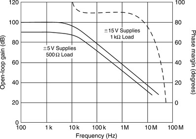
The open-loop gain is the gain of the amplifier when the feedback loop is not closed. It is generally measured, however, with the feedback loop closed, although at a very large gain. In an ideal op amp, it is infinite with infinite bandwidth. In practice, it is very large (up to 160 dB) at DC. At some frequency (the dominant pole) it starts to fall at 6 dB/octave or 20 dB/decade. (An octave is a doubling in frequency and a decade is × 10 in frequency.) This is referred to as a single pole response. The dominant pole frequency will range from in the neighborhood of 10 Hz for some high precision amps to several kHz for some high speed amps. It will continue to fall at this rate until it reaches another pole in the response. This second pole will double the rate at which the open-loop gain falls, that is to 12 dB/octave or 40 dB/decade. If the open-loop gain has gone below 0 dB (unity gain) before the amp hits the second pole, the op amp will be unconditionally stable at any gain. This will be referred to as unity gain stable on the data sheet. If the second pole is reached while the loop gain is greater than 1 (0 dB), then the amplifier may not be stable under some conditions (Figure 1-27).
Since the open-loop gain falls by half with a doubling of frequency with a single pole response, there is what is called a constant gain-bandwidth product. At any point along the curve, if the frequency is multiplied by the gain at that frequency, the product is a constant. For example, if an amplifier has a 1 MHz gain-bandwidth product, the open-loop gain will be 10 (20 dB) at 100 kHz, 100 (40 dB) at 10 kHz, etc. This is readily apparent on a Bode plot, which plots gain versus frequency on a log–log scale.
Since a VFB op amp operates as a voltage in/voltage out device, its open-loop gain is a dimensionless ratio, so no unit is necessary. Data sheets sometimes express gain in V/mV or V/μV instead of V/V, for the convenience of using smaller numbers. Or voltage gain can also be expressed in dB terms, as gain in dB = 20 × log AVOL. Thus an open-loop gain of 1 V/μV (or 1000 V/mV or 1,000,000 V/V) is equivalent to 120 dB, and so on (Figure 1-28).
For very high precision work, the nonlinearity of the open-loop gain must be considered. Changes in the output voltage level and output loading are the most common causes of changes in the open-loop gain of op amps. A change in open-loop gain with signal level produces a nonlinearity in the closed-loop gain transfer function, which cannot be removed during system calibration. Most op amps have fixed loads, so AVOL changes with load are not generally important. However, the sensitivity of AVOL to output signal level may increase for higher load currents (see Figure 1-29).

The severity of this nonlinearity varies widely from one device type to another, and generally is not specified on the data sheet. The minimum AVOL is always specified, and choosing an op amp with a high AVOL will minimize the probability of gain nonlinearity errors. There is no way to compensate for AVOL nonlinearity.
Open-Loop Transresistance of a CFB Op Amp
For CFB amplifiers, the open-loop response is voltage out for a current in, so it is a transresistance (expressed in ohms) rather than a gain. This is generally referred to as a transimpedance, since there is an AC component as well as a DC term. The transimpedance of a CFB amp will usually be in the range of 500 kΩ to 1 MΩ.
A CFB op amp open-loop transimpedance does not vary in the same way as a VFB open-loop gain. Therefore, a CFB op amp will not have the same gain-bandwidth product as in VFB amps. While there is some variation of frequency response with frequency with a CFB amp, it is nowhere near 6 dB/octave (see Figure 1-30).

When using the term transimpedance amplifier, there can be some confusion. An amplifier configured as a current to voltage (I/V) converter, typically in photodiode circuits, is also referred to as a transimpedance amplifier. But the photodiode application will generally use a FET input VFB amp rather than a CFB amp. This is because the current levels in the photodiode applications will be very low, not the most compatible with the low impedance input of a CFB op amp.
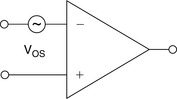
Offset Voltage
If both inputs of an op amp are at exactly the same voltage, then the output should be at zero volts, since a differential of 0 V should produce an output of 0V. In practice, however, there will typically be some voltage at the output. This is known as the offset voltage or VOS. The typical way to specify offset voltage is as the amount of voltage that must be added to the input to force 0V out. This voltage, divided by the noise gain of the circuit, is the input offset voltage or input referred offset voltage. The offset voltage is usually input referred to eliminate the effect of circuit gain, which makes comparisons easier. The offset voltage is modeled as a voltage source, VOS, in series with the inverting input of the op amp as shown in Figure 1-31.
Offset Voltage Drift
The input offset voltage varies with temperature. Its temperature coefficient is known asTCVOS, or more commonly, drift. Offset drift may be as low as 0.1 μV/°C (typical value for OP-177F, a very high precision op amp). More typical drift values for a range of general purpose precision op amps lie in the range 1–10 μV/°C. Most op amps have a specified value of TCVOS, but some, instead, have a second value of maximum VOS that is guaranteed over the operating temperature range. Such a specification is less useful, because there is no guarantee that TCVOS is constant or monotonic.
Drift with Time
The offset voltage also changes as time passes, or ages. Aging is generally specified in μV/month or μV/1000 hours, but this can be misleading. Aging is not linear, but instead a nonlinear phenomenon that is proportional to the square root of the elapsed time. A drift rate of 1 μV/1000 hours therefore becomes about 3 μV/year (not 9 μV/year). Long-term drift of the OP-177F is approximately 0.3 μV/month. This refers to a time period after the first 30 days of operation. Excluding the initial hour of operation, changes in the offset voltage of these devices during the first 30 days of operation are typically less than 2 μV. The long-term drift of offset voltage with time is not always specified, even for precision op amps.
Correction for Offset Voltage
Early op amps typically had pins available for nulling out offset voltages. A potentiometer connected to these pins, and the wiper connected to one or the other of the supply voltages, allowed balancing the input stage, which, in turn, nulled out the offset voltage (see Figure 1-32).

Makers of high precision op amps, such as Analog Devices (ADI) and Precision Monolithics (PMI) employed circuit design tricks to internally balance the input structures. ADI used laser trimming of the input stage load resistors to achieve balance. PMI used a technique called zener zapping to accomplish basically the same thing.
Laser trimming used lasers to eat away part of the collector resistors to adjust their value. Zener zapping involved having a string of resistors, each bypassed by a semiconductor structure that is basically a zener diode. By applying a pulse of voltage these zener diodes would be shorted out (zapped). This adjusts the value of the resistor string.
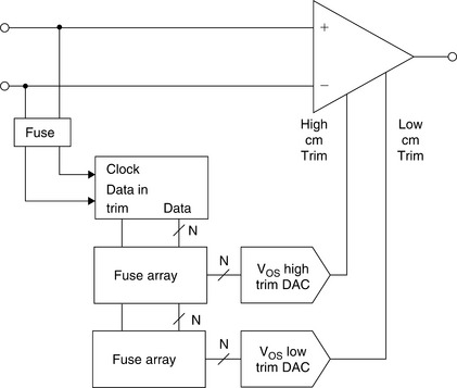
DigiTrim™ Technology
DigiTrim is a technique which adjusts circuit offset performance by programming digitally weighted current sources, in essence a DAC. This technique makes use of the mixed signal capabilities of the CMOS process. While, historically, CMOS would not be the first choice for precision amplifiers, recent process improvements combined with the DigiTrim technology result in a very reasonable precision performance. In this patented new trim method, the trim information is entered through existing analog pins using a special digital keyword sequence. The adjustment values can be temporarily programmed, evaluated, and readjusted for optimum accuracy before permanent adjustment is performed. After the trim is completed, the trim circuit is locked out to prevent the possibility of any accidental re-trimming by the end user.
A unique feature of this technique is that the adjustment is done after the chip is packaged. With zener zapping and laser trimming, the offset must be adjusted at the die level. Subsequent processing, mounting the chip on a header and encapsulating in plastic cause a shift in the offset. This is due to both the mechanical stress of the mounting (strain gauge effect) and the heat of molding the package. While the amount of the shift is well profiled, the ability to trim at the package level versus the chip level is a distinct advantage.
The physical trimming, achieved by blowing polysilicon fuses, is very reliable. No extra pads or pins are required for this trim method and no special test equipment is needed to perform the trimming. The trimming is done through the input pins. A simplified representation of an amplifier with DigiTrim™ is shown in Figure 1-33. No testing is required at the wafer level assuming reasonable die yields. No special wafer fabrication process is required and circuits can even be produced by our foundry partners. All of the trim circuitry tend to scale with the process features so that as the process and the amplifier circuit shrink, the trim circuit also shrinks proportionally. The trim circuits are considerably smaller than normal amplifier circuits so that they contribute minimally to die cost. The trims are discrete as in link trimming and zener zapping, but the required accuracy is easily achieved at a very small cost increase over an untrimmed part.
The DigiTrim approach could also support user trimming of system offsets with a different amplifier design. This has not yet been implemented in a production part, but it remains a possibility.
External Trim
The offset adjustment pins started to disappear with the advent of dual op amps since there were not enough pins left for them in the 8-pin package. Therefore external adjustment techniques were required.
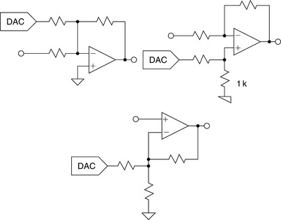
External trimming out offset involves basically adding a small voltage to the input to counteract the offset (see Figure 1-34). The polarity of the voltage applied to the offset pot will depend on the process used to manufacture the part as well as the polarity of the input devices (NPN or PNP). The offset can be accomplished with potentiometers, digital pots, or DACs. The major problem with external trimming is that the temperature coefficients of the internal and external components will probably not match. This will limit the effectiveness of the adjustment over temperature.

In addition, the mechanical pot is subject to aging and mechanical vibration.
There is an increase in noise gain due to the added resistance and the potentiometer resistance. The resulting increase in noise gain may be reduced by making R3 much greater than R1. Note that otherwise, the signal gain might be affected as the offset potentiometer is adjusted. The gain may be stabilized, however, if R3 is connected to a fixed low impedance reference voltage sources, ± VR.
The digital pot and DAC, however, can be adjusted in circuit, under control of a microprocessor or microcontroller, which could mitigate aging and temperature effects (Figure 1-35).
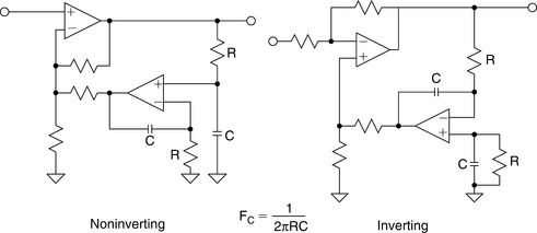
If response to DC is not required, an alternative approach would be to use a circuit called a servo (see Figure 1-36). This circuit is basically an integrator, which is placed in a feedback loop around the main amplifier. A precision amplifier should be used for the integrator; it need not be fast enough to pass the full frequency spectrum that the main amplifier must. The circuit operates by taking the average DC level of the output and feeding it back to the main amplifier, in effect subtracting it from the signal.
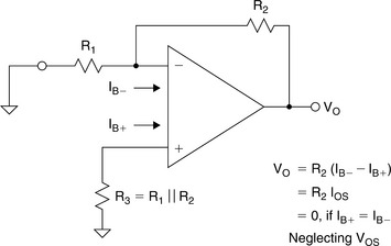
Input Bias Current
In the ideal model of the op amp the inputs have infinite impedance and so no current flows into the input terminals. But since the most common input structure uses bipolar junction transistors (BJTs), there is always some current required for operation, since the BJT is a current controlled device. This is referred to as bias current (IB) or input bias current. In practice, there are always two input bias currents, IB+ and IB− (see Figure 1-37), one for each of the inputs. Values of IB range from 60 fA (about one electron every three microseconds) in the AD549 electrometer, to tens of microamperes in some high speed op amps. Due to the inherent nature of monolithic op amp fabrication processing, these bias currents tend to be equal, but this is not guaranteed to be case. And in the case of CFB amplifiers, the non-symmetric nature of the inputs guarantees that the bias currents are different.

Input bias current is a problem to the op amp user because it flows in external impedances and produces offset voltages, which add to system errors. Consider a non-inverting unity gain buffer driven from a source impedance of 1 MΩ. If IB is 10 nA, it will introduce an additional 10 mV of error. Or, if the designer simply forgets about IB and uses capacitive coupling, the circuit will not work at all! This is because the bias currents need a DC return path to ground. If the DC return path is not there, the input of the op amp will drift to one of the rails. Or, if IB is low enough, it may work momentarily while the capacitor charges, giving even more misleading results. The moral here is not to neglect the effects of IB in any op amp circuit.
Input Offset Current
The difference in the bias currents is the input offset current. Normally the difference between the bias currents is small, so that the offset current is also small. In bias-compensated op amps (see next section) the offset current is approximately equal to the bias current.
Compensating for Input Bias Current
There are several ways to compensate for bias currents. It can be addressed by the manufacturer, or external techniques can be employed.
There are basically two different ways that an IC manufacturer can deal with bias currents.
The first is to use a “super-beta” transistors for the input stage. Super-beta transistors are specially processed devices with a very narrow base region. They typically have a current gain (β) of thousands or tens of thousands (rather than the more usual hundreds for standard BJT transistors). Op amps with super-beta input stages have much lower bias currents, but they also have more limited frequency response. Since the breakdown voltages of super-beta devices are typically quite low, they also require additional circuitry to protect the input stage from damage caused by overvoltage on the input.
The second method of dealing with bias currents is to use a bias-compensated input structure (see Figure 1-38). With a bias current compensated input, small current sources are added to the bases of the input devices. The idea is that the bias currents required by the input devices are provided by the current sources so that the net current seen by the external circuit is reduced considerably.

Bias current compensated input stages have many of the good features of the simple bipolar input stage, namely: low voltage noise, low offset, and low drift. Additionally, they have low bias current which is fairly stable with temperature. However, their current noise is not very good, since current sources are added to the input. And their bias current matching is poor. These latter two undesired side effects result from the external bias current being the difference between the compensating current source and the input transistor base current. Both of these currents inevitably have noise. Since they are uncorrelated, the two noises add in a root-sum-of-squares fashion (even though the DC currents subtract).
Note that this can easily be verified, by examining the offset current specification (the difference in the bias currents). If internal bias current compensation exists, the offset current will be of the same magnitude as the bias current. Without bias current compensation, the offset current will generally be at least a factor of 10 smaller than the bias current. Note that these relationships generally hold, regardless of the exact magnitude of the bias currents.
Since the resulting external bias current is the difference between two nearly equal currents, there is no reason why the net current should have a defined polarity. As a result, the bias currents of a bias-compensated op amp may not only be mismatched, they can actually flow in opposite directions! In most applications this is not important, but in some it can have unexpected effects (e.g., the droop (change of voltage in the hold mode) of a sample-and-hold amplifier (SHA) built with a bias-compensated op amp may have either polarity).
In many cases, the bias current compensation feature is not mentioned on an op amp data sheet. It is easy to determine if bias current compensation is being used by examining the bias current specification. If the bias current is specified as a “±” value, the op amp is most likely compensated for bias current.
The designer can compensate for the effects of the bias current by equalizing the impedances seen by the two inputs (see Figure 1-39). If the impedances are equal, then the bias currents (which will tend to also be equal) flowing through them will produce the same offset voltage, which will appear as a common-mode signal. Since it is a common-mode signal it would tend not to add to the error due to the common-mode rejection (CMRR, to be discussed later in this section) of the amplifier.
Care should be used when applying this technique. It obviously will not work with a bias-compensated op amp, since the bias currents are not equal. With FET input amps, the impedance levels tend to be high and the bias currents are small, so the added effects of the Johnson noise of the high input impedances might be worse than the effects of the bias current flowing through them. Analysis needs to be performed.
Calculating Total Output Offset Error Due to IB and VOS
The equations shown in Figure 1-40 below are useful in referring all the offset voltage and induced offset voltage from bias current errors to the either the input (RTI) or the output (RTO) of the op amp. The choice of RTI or RTO is a matter of preference.

The RTI value is useful in comparing the cumulative op amp offset error to the input signal. The RTO value is more useful if the op amp drives additional circuitry, to compare the net errors with those of the next stage. In any case, the RTO value is simply obtained by multiplying the RTI value by the stage noise gain, which is 1 + R2/R1.
There are some simple rules towards minimization offset voltage and bias current errors. First, keep input/feedback resistance values low, to minimize offset voltage due to bias current effects. Second, use bias compensation resistors. Bypass these resistors with fairly large values of capacitance. This gives the advantage of the resistors at DC for bias currents, but shorts out the resistances at higher frequencies to minimize noise at higher frequencies. Next, it is probably not wise to use this technique with FET input devices, since the value of the compensation resistor will likely add more noise than it will save in bias current compensation. If an op amp uses internal bias current compensation, do not use the compensation resistance, since the bias currents will not match. When necessary, use external offset trim networks, for lowest induced drift. Select an appropriate precision op amp specified for low offset and drift, as opposed to trimming.
Input Impedance
VFB op amps normally have both differential and common-mode input impedances specified. CFB op amps normally specify the impedance to ground at each input. Different models may be used for different VFB op amps, but in the absence of other information, it is usually safe to use the model in Figure 1-41. In this model the bias currents flow into the inputs from infinite impedance current sources.
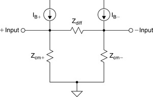
The common-mode input impedance data sheet specification (Zcm+ and Zcm−) is the impedance from either input to ground (NOT from both to ground). The differential input impedance (Zdiff) is the impedance between the two inputs. These impedances are usually resistive and high (105–1012 Ω.) with some shunt capacitance (generally a few pF, sometimes 20–25 pF). In most op amp circuits, the inverting input impedance is reduced to a very low value by negative feedback, and only Zcm+ and Zdiff are of importance.
A CFB op amp is even more simple, as shown in Figure 1-42. Z+ is resistive, generally with some shunt capacitance, and high (105–109 Ω) while Z− is reactive (L or C, depending on the device) but has a resistive component of 10–100 Ω, varying from type to type.

Input Capacitance
In general, the input capacitance is not an issue with high speed op amps. In certain applications, such as a photodiode amp, where the source impedance is high, it could come into play. With a very large source impedance, a relatively small capacitance could set up a zero in the transmission function. This could lead to instability. Since the noise gain of the amplifier is rising a 6 dB/octave, and the open-loop gain is falling at 6 dB/octave, the intersection will be at 12 dB/octave, which is unstable.
Another issue with FET input devices driven from a high impedance source in the non-inverting configuration is the modulation of the input capacitance by the common-mode voltage. This leads to a level dependent distortion. To compensate for this effect, balancing the impedances as seen by the inputs is used. This is similar to the balancing used for input bias current, except that the balance is not just for DC.
Input Common-Mode Voltage Range
The input common-mode range is the allowable voltage on the input pins. It usually is not the full supply range. Classical system design used ± 15 V supplies with an expected dynamic range of ± 10 V, so the inputs really needed only to cover those ranges.
However, the current trend is to smaller and smaller supply voltages. This increases the need to maximize the input dynamic range. Many low voltage op amps utilize “rail-to-rail” inputs. While there is no industry standard definition for “rail-to rail,” at ADI it is defined as swinging within 100 mV of either rail. Note that not all devices marketed as single supply are rail-to-rail, and not all devices that are marketed as rail-to-rail are able to swing to the rails on both input and output. You must read the data sheet carefully.
Certain inputs, such as bias-compensated and super-beta op amps, will further limit the input voltage range.
Differential Input Voltage
Certain input structures require limiting of differential input voltage to prevent damage. These op amps will generally have back-to-back diodes across the inputs. This will not always show up in the simplified schematics of the amps. It will show up, however, as a differential input voltage specification of ±700 mV maximum.
In addition you may find a specification for the maximum input differential current. Some amps have current limiting resistors built in, but these resistors raise the noise, so for low noise op amps there are left off.
Supply Voltage
Classical system design was ± 15 V supplies with an expected signal dynamic range of ± 10 V. Most early op amps were designed to operate on these voltages. The supply voltage typically had a very wide range. On the data sheet a range of allowable supply voltages was generally listed. It could be something like ±4.5 V to ± 18 V, which is the specification for the AD712. In general there are some small changes in the specifications for the same op amp operated on different supplies. This usually shows up as multiple specification pages, each at a different set of conditions, which usually means different supplies.
Although the voltage specification was generally given as a symmetrical bipolar voltage, there is no reason that it had to be either symmetrical or bipolar. To the op amp a ±15 V supply is the same as a + 30/0 V supply or a + 20/− 10 V supply, as long as the inputs are biased in the active region (within the common-mode range).
The current trend is to lower supply voltages. For high speed amps this is partially due to process limitations. Higher speeds imply small physical structures, which, in turn, imply lower breakdown voltages. Lower breakdown voltages imply lower supply voltages. Currently most high speed op amps require ± 5 V or single +5 V supplies. For general purpose op amps, supplies are getting as low as + 1.8 V. Note that the term single supply is sometimes used to indicate lower supply voltages. The two concepts are related, but, as pointed out above, single supply does not necessarily mean low voltage. Keep the concepts separate.
CMOS op amps are also generally operated with lower supplies. The trend in CMOS processes, again driven by digital circuits, emphasizes small and smaller geometries, with their attendant lower breakdown voltages.
Quiescent Current
The quiescent current is the current internally consumed by the op amp itself (no load). In general, high speed amps tend to draw more quiescent current than general purpose amps. In addition, for general purpose op amps, some performance parameters (noise and distortion in particular) tend to improve with higher current. On the other end of the spectrum, the lowest quiescent current amps have severely limited bandwidth. Currently the lowest quiescent current device from ADI is the OP-290 at 3.5 μA.
There is a strong demand for low quiescent current op amps. One driving application is battery powered equipment. While there is no industry standard for what “low power” means, at ADI “low power” is defined as less than 1 mA of quiescent current. “Micropower” is defined as less than 100 μA quiescent current. Note that this is per amplifier, so a quad op amp will draw 4× this amount. Also note that this applies only to amplifiers. Low power can mean many things to many people. For instance a very high speed analog-to-digital converter (ADC) may dissipate over 1W! This can still be considered low power, since competing solutions can be over 4 W.
Output Voltage Swing (Output Voltage High/Output Voltage Low)
As pointed out above, classical system design used ± 15 V supplies with an expected dynamic range of ± 10 V. The standard output structure was an emitter follower (common collector) circuit. The base is a diode drop above the output. There must be some voltage above that for biasing the drive signal. So we need a specification on how much voltage we can expect from the output. If using reduced supply voltages, this specification for overhead will remain constant. For example, if the specification is ± 12 V (minimum) on a ± 15 V supply, we should expect to achieve ±6 V on a ±9 V supply.
Again, as we shrink the supply voltage, we need to maximize the output dynamic range. After all, if we lose 3 V to each of the supply rails, as in the example above, and we are operating on a ± 3 V supply, we will have a severely compressed dynamic range. What is typically done to increase the dynamic range is to change the configuration of the output stage from an emitter follower to a common emitter. The output will then be able to swing to within the VCEsat of the output transistor.
Allowing the output to swing close to the rail is referred to as “rail-to-rail.” As we discussed in the input voltage section, there is no industry standard rail-to-rail specification. At ADI we define it, again, as being able to swing within 100 mV of either rail, with the added constraint of driving a 10 kΩ load. The value of the load is important, since the VCEsat of the output transistor is dependent on output current. Remember not all “single supply” op amps are “rail-to-rail” and not all “rail-to-rail” are so on both input and output. You must read the data sheet.
Output Current (Short Circuit Current)
Most general purpose op amps have output stages which are protected against short circuits to ground or to either supply. This is commonly referred to as “infinite” short circuit protection, since the amplifier can drive that value of current into the short circuit indefinitely. The output current that can be expected to be delivered by the op amp is the output current. Typically the limit is set so that the op amp can deliver 10 mA for general purpose op amps.
If an op amp is required to have both high precision and a large output current, it is advisable to use a separate output stage (within the feedback loop) to minimize self-heating of the precision op amp. This added amplifier is often called a buffer, since it typically will have a voltage gain = 1.
There are some op amps that are designed to give large output currents. An example is the AD8534, which is a quad device that has an output current of 250 mA for each of the four sections. A word of warning: if you try to supply 250 mA from of all four sections at the same time, you will exceed the package dissipation specification. The amp will overheat, and could destroy itself. This problem gets worse with smaller packages, which have lower dissipation.
High speed op amps typically do not have output currents limited to a low value, since it would affect their slew rate and ability to drive low impedances. Most high speed op amps will source and sink between 50–100 mA, though a few are limited to less than 30 mA. Even for high speed op amps that have short circuit protection, junction temperatures may be exceeded (because of the high short circuit current) resulting in device damage for prolonged shorts.
AC Specifications
Noise
This section discusses the noise generated within op amps, not external noise which they may pick up. External noise is important, and is discussed in detail in other texts, but in this section we are concerned solely with internal noise.
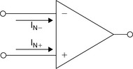
There are three noise sources in an op amp: a voltage noise, which appears differentially across the two inputs and a current noise in each input. These sources are effectively uncorrelated (independent of each other). In fact, there is a slight correlation between the two noise currents, but it is too small to need consideration in practical noise analyses. In addition to these three internal noise sources, it is necessary to consider the Johnson noise of the external resistors, which are used with the op amp in the feedback network.
Voltage Noise
The voltage noise of different op amps may vary from under 1 to 20 nV/![]() , or even more. Bipolar op amps tend to have lower voltage noise than JFET amps. Voltage noise is specified on the data sheet, and it is not possible to predict it from other parameters (Figure 1-43).
, or even more. Bipolar op amps tend to have lower voltage noise than JFET amps. Voltage noise is specified on the data sheet, and it is not possible to predict it from other parameters (Figure 1-43).

Until recently, JFET input amplifiers tended to have comparatively high voltage noise (though they have very low current noise), and were thus more suitable for low noise applications in high impedance rather than low impedance circuitry. The AD645 and AD743/AD745 have very low values of both voltage and current noise. The AD645 specifications at 10 kHz are 10 nV/![]() and 0.6 fA/
and 0.6 fA/![]() , and the AD743/AD745 specifications at 10 kHz are 2.9 nV/
, and the AD743/AD745 specifications at 10 kHz are 2.9 nV/![]() and 6.9 fA/
and 6.9 fA/![]() . These make possible the design of low noise amplifier circuits, which have low noise over a wide range of source impedances. The cost of the lower voltage noise is large input devices, and hence large input capacitance.
. These make possible the design of low noise amplifier circuits, which have low noise over a wide range of source impedances. The cost of the lower voltage noise is large input devices, and hence large input capacitance.
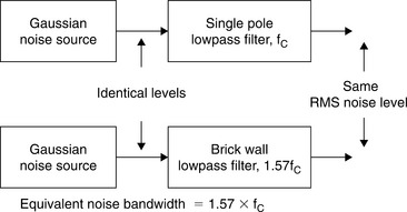
Noise Bandwidth
When calculating the bandwidth of the noise contribution we always use a bandwidth of 1.57 fc to calculate the noise. The reason for this is that a Gaussian (white) noise source passed through a single pole filter with a cutoff frequency of fc has the same spectral energy as the same source passed through a brick wall filter with a cutoff frequency of 1.57 fc. A brick wall filter has a flat response up to the cutoff frequency above which it has infinite attenuation. Similarly, a two pole filter has an apparent corner frequency of approximately 1.2 fc. The error correction factor is usually negligible for filters having more than two poles (Figure 1-44).
Noise Figure
Noise figure is rarely used with op amps. The noise figure of an amplifier is the amount (in dB) by which the noise of the amplifier exceeds the noise of a perfect noise-free amplifier in the same environment. The concept comes from RF and TV applications, where 50 or 75 Ω transmission lines and terminations are ubiquitous, but is useless for an op amp, which may be used with a wide variety of impedances. Voltage noise spectral density and current noise spectral density are much more useful specifications.
Current Noise
Current noise can vary much more widely, from around 0.1 fA/![]() (in JFET electrometer op amps) to several pA/
(in JFET electrometer op amps) to several pA/![]() (in high speed bipolar op amps). It is not always specified on data sheets, but may be calculated in cases (like simple BJT or JFET input devices) where all the bias current flows in the input junction, because in these cases it is simply the Schottky (or shot) noise of the bias current. It cannot be calculated for bias-compensated or CFB op amps, where the external bias current is the difference of two internal current sources. The shot noise spectral density is simply
(in high speed bipolar op amps). It is not always specified on data sheets, but may be calculated in cases (like simple BJT or JFET input devices) where all the bias current flows in the input junction, because in these cases it is simply the Schottky (or shot) noise of the bias current. It cannot be calculated for bias-compensated or CFB op amps, where the external bias current is the difference of two internal current sources. The shot noise spectral density is simply ![]() , where IB is the bias current (in amps) and q is the charge on an electron (1.6 × 10⁻¹⁹C) (Figure 1-45).
, where IB is the bias current (in amps) and q is the charge on an electron (1.6 × 10⁻¹⁹C) (Figure 1-45).
The current noise for the inputs of a VFB op amp are uncorrelated and roughly equal in value. In the simple input structures, the current noise is the shot noise of the input bias current. In a Bias-Compensated op amp, the current noise cannot be calculated. Also, since the inputs of a CFB op amp are different, the current noise for the two inputs can be very different. The 1/f corners will typically not match either.
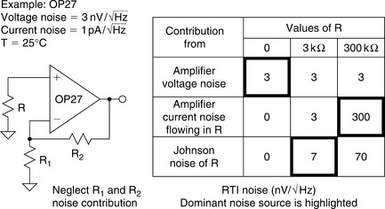
Current noise is only important when it flows in an impedance and generates a noise voltage. Therefore, the choice of a low noise op amp depends on the impedances around it. Consider an OP-27, a bias-compensated op amp with low voltage noise (3 nV/![]() ), but quite high current noise (1 pA/
), but quite high current noise (1 pA/![]() ). With zero source impedance, the voltage noise will dominate. With a source resistance of 3 kΩ, the current noise (1 pA/
). With zero source impedance, the voltage noise will dominate. With a source resistance of 3 kΩ, the current noise (1 pA/![]() flowing in 3 kΩ) will equal the voltage noise, but the Johnson noise of the 3 kΩ resistor is 7 nV/
flowing in 3 kΩ) will equal the voltage noise, but the Johnson noise of the 3 kΩ resistor is 7 nV/![]() and so is dominant. With a source resistance of 300 kΩ, the current noise increases a hundredfold to 300 nV/
and so is dominant. With a source resistance of 300 kΩ, the current noise increases a hundredfold to 300 nV/![]() , while the voltage noise continues unchanged, and the Johnson noise (which is proportional to the square root of the resistance) only increases ten-fold. Here, current noise is dominant.
, while the voltage noise continues unchanged, and the Johnson noise (which is proportional to the square root of the resistance) only increases ten-fold. Here, current noise is dominant.
Total Noise (Sum of Noise Sources)
Uncorrelated noise voltages add in a “root-sum-of-squares” manner; i.e., noise voltages V1, V2, V3 give a summed result of ![]() . Noise powers, of course, add normally. Thus, any noise voltage that is more than 3–5 times any of the others is dominant, and the others may generally be ignored. This simplifies noise assessment. Current noises flowing through resistance equal noise voltages (Figure 1-46).
. Noise powers, of course, add normally. Thus, any noise voltage that is more than 3–5 times any of the others is dominant, and the others may generally be ignored. This simplifies noise assessment. Current noises flowing through resistance equal noise voltages (Figure 1-46).

The choice of a low noise op amp depends on the source impedance of the signal, and at high impedances, current noise always dominates.
For low impedance circuitry, amplifiers with low voltage noise, such as the OP-27, will be the obvious choice, since they are inexpensive, and their comparatively large current noise will not affect the application (see Figure 1-47). At medium resistances, the Johnson noise of resistors is dominant, while at very high resistances, we must choose an op amp with the smallest possible current noise, such as the FET input devices AD549 or AD645.
1/f Noise (Flicker Noise)
So far, we have assumed that noise is white (i.e., its spectral density does not vary with frequency). This is true over most of an op amp’s frequency range, but at low frequencies the noise spectral density rises at 3 dB/octave, as shown in Figure 1-48. The power spectral density in this region is inversely proportional to frequency, and therefore the voltage noise spectral density is inversely proportional to the square root of the frequency. For this reason, this noise is commonly referred to as 1/f noise. Note, however, that some textbooks still use the older term flicker noise.
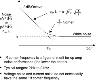
The frequency at which this noise starts to rise is known as the 1/f corner frequency (FC) and is a figure of merit—the lower it is, the better. The 1/f corner frequencies are not necessarily the same for the voltage noise and the current noise of a particular amplifier, and a CFB op amp may have three 1/f corners: for its voltage noise, its inverting input current noise, and its non-inverting input current noise.
The general equation which describes the voltage or current noise spectral density in the 1/f region is:
where k is the level of the “white” current or voltage noise level, and FC is the 1/f corner frequency.
The best low frequency low noise amplifiers have corner frequencies in the range 1–10 Hz, while JFET devices and more general purpose op amps have values in the range 100 Hz to sometimes over 1 kHz. Very fast amplifiers, however, may make compromises in processing to achieve high speed which result in quite poor 1/f corners of several hundred Hz or even 1–2 kHz. This is generally unimportant in the wideband applications for which they were intended, but may affect their use at audio frequencies, particularly in equalization circuits (Figure 1-49).

Popcorn Noise
Popcorn noise is so-called because when played through an audio system, it sounds like cooking popcorn. It consists of random step changes of offset voltage that take place at random intervals in the 10+ millisecond timeframe. Such noise results from high levels of contamination and crystal lattice dislocation at the surface of the silicon chip, which in turn results from inappropriate processing techniques or poor quality raw materials. When monolithic op amps were first introduced in the 1960s, popcorn noise was a dominant noise source. Today, however, the causes of popcorn noise are well understood, raw material purity is high, contamination is low, and production tests for it are reliable so that no op amp manufacturer should have any difficulty in shipping products that are substantially free of popcorn noise. For this reason, it is not even mentioned in most modern op amp textbooks or data sheets.
RMS Noise Considerations
As was discussed above, noise spectral density is a function of frequency. In order to obtain the RMS noise, the noise spectral density curve must be integrated over the bandwidth of interest.
In the 1/f region, the RMS noise in the bandwidth f1 to f2 is given by:
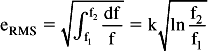 (1-16)
where k is the noise spectral density at 1 Hz. The total 1/f noise in a given band is a function of the ratio of the low and high band edge frequencies, since the actual frequency cancels out. It is necessary, however, that the upper band edge is still in the 1/f region for the above formula to be accurate.
It is often desirable to convert RMS noise measurements into peak-to-peak. In order to do this, one must have some understanding of the statistical nature of noise. For Gaussian noise and a given value of RMS noise, statistics tell us that the chance of a particular peak-to-peak value being exceeded decreases sharply as that value increases—but this probability never becomes zero.
Thus, for a given RMS noise, it is possible to predict the percentage of time that a given peak-to-peak value will be exceeded, but it is not possible to give a peak-to-peak value which will never be exceeded as shown in Figure 1-50.

Peak-to-peak noise specifications, therefore, must always be given for a specified time limit. The most common choice is for the peak-to-peak noise to be 6.6 times the RMS value, which is means the peak-to-peak level will be exceeded only 0.1% of the time.
In many cases, the low frequency noise is specified as a peak-to-peak value within the bandwidth 0.1–10 Hz. This is measured by inserting a 0.1–10 Hz bandpass filter between the op amp and the measuring device. The measurement is often presented as a scope photo with a time scale of 1 s/division as shown in Figure 1-51 for the OP-213.

In practice, it is virtually impossible to measure noise within specific frequency limits with no contribution from outside those limits, since practical filters have finite rolloff characteristics. Fortunately, the measurement error introduced by a single pole lowpass filter is readily computed. See the previous section on noise bandwidth.
When computing RMS noise for wide bandwidth op amps, 1/f noise becomes relatively insignificant. The dominant source of noise is Gaussian, or white noise. This noise has a relatively constant noise spectral density over a wide range of frequencies. The RMS noise calculation is made by multiplying the noise spectral density by the square root of the equivalent noise bandwidth.
Total Output Noise Calculations
We have already pointed out that any noise source which produces less than one-third to one-fifth of the noise of some other source can be ignored. (Both noise voltages must be measured at the same point in the circuit.) To analyze the noise performance of an op amp circuit, we must assess the noise contributions of each part of the circuit and determine which are significant. To simplify the following calculations, we shall work with noise spectral densities, rather than actual voltages, to leave bandwidth out of the expressions (the noise spectral density, which is generally expressed in μV/![]() , is equivalent to the noise in a 1 Hz bandwidth).
, is equivalent to the noise in a 1 Hz bandwidth).
All resistors have a Johnson noise of ![]() , where k is Boltzmann’s Constant (1.38 × 10⁻²³ J/K), T is the absolute temperature, B is the bandwidth and R is the resistance. This is intrinsic—it is not possible to obtain resistors which do not have Johnson noise (unless operated a 0°K) (Figure 1-52).
, where k is Boltzmann’s Constant (1.38 × 10⁻²³ J/K), T is the absolute temperature, B is the bandwidth and R is the resistance. This is intrinsic—it is not possible to obtain resistors which do not have Johnson noise (unless operated a 0°K) (Figure 1-52).

If we consider the circuit in Figure 1-53, which is an amplifier consisting of an op amp and three resistors (Rp represents the source resistance at node A), we can find six separate noise sources: the Johnson noise of the three resistors, the op amp voltage noise, and the current noise in each input of the op amp. Each has its own contribution to the noise at the amplifier output. (Noise is generally specified RTI, or referred to the input, but it is often simpler to calculate the noise at the output and then divide it by the signal gain [not the noise gain] of the amplifier to obtain the RTI noise.)

The circuit in Figure 1-54 represents a second-order system, where capacitor C1 represents the source capacitance, stray capacitance on the inverting input, the input capacitance of the op amp, or any combination of these. C1 causes a breakpoint in the noise gain, and C2 is the capacitor which must be added to obtain stability. Because of C1 and C2, the noise gain is a function of frequency, and has peaking at the higher frequencies (assuming C2 is selected to make the second-order system critically damped).

A DC signal applied to input A (B being grounded) sees a gain of:
At higher frequencies, the gain from input A to the output becomes:
The closed-loop bandwidth fc1 is the point at which the Noise Gain intersects the open-loop gain. A DC signal applied to B (A being grounded) sees a gain of:
with a high frequency cutoff determined by R2C2:
These are the non-inverting and inverting gains and bandwidths, respectively, of the amplifier (Figure 1-55).

The current noise of the non-inverting input, In+, flows in Rp and gives rise to a noise voltage of In + Rp, which is amplified by Eqs (1-17 and 1-18), as are the op amp noise voltage, Vn, and the Johnson noise of Rp, which is ![]() . The Johnson noise of R1 is amplified by Eq. (1-19) over a bandwidth of 1/2(πR2C2) Eq. (1-20), and the Johnson noise of R2 is not amplified at all but is buffered directly to the output over a bandwidth of 1/2(πR2C2). The current noise of the inverting input, In_, does not flow in R1, as might be expected—negative feedback around the amplifier works to keep the potential at the inverting input unchanged, so that a current flowing from that pin is forced, by negative feedback, to flow in R2 only, resulting in a voltage at the amplifier output of In_R2 over a bandwidth of 1/2(πR2C2) (we could equally well consider the voltage caused by In_ flowing in the parallel combination of R1 and R2 and then amplified by the noise gain of the amplifier [see below], but the results are identical—only the calculations are more involved).
. The Johnson noise of R1 is amplified by Eq. (1-19) over a bandwidth of 1/2(πR2C2) Eq. (1-20), and the Johnson noise of R2 is not amplified at all but is buffered directly to the output over a bandwidth of 1/2(πR2C2). The current noise of the inverting input, In_, does not flow in R1, as might be expected—negative feedback around the amplifier works to keep the potential at the inverting input unchanged, so that a current flowing from that pin is forced, by negative feedback, to flow in R2 only, resulting in a voltage at the amplifier output of In_R2 over a bandwidth of 1/2(πR2C2) (we could equally well consider the voltage caused by In_ flowing in the parallel combination of R1 and R2 and then amplified by the noise gain of the amplifier [see below], but the results are identical—only the calculations are more involved).
If we consider these six noise contributions, we see that if Rp and R2 are low, then the effect of current noise and Johnson noise will be minimized, and the dominant noise will be the op amp’s voltage noise. As we increase resistance, both Johnson noise and the voltage noise produced by noise currents will rise. If noise currents are low, then Johnson noise will take over from voltage noise as the dominant contributor. Johnson noise, however, rises with the square root of the resistance, while the current noise voltage rises linearly with resistance, so ultimately, as the resistance continues to rise, the voltage due to noise currents will become dominant.
These noise contributions we have analyzed are not affected by whether the input is connected to node A or node B (the other being grounded or connected to some other low impedance voltage source), which is why the non-inverting gain (1 + R2/R1), which is seen by the voltage noise of the op amp, Vn, is known as the “noise gain” of the amplifier.
Calculating the total output RMS noise of the op amp requires multiplying each of the six noise voltages by the appropriate gain and integrating over the appropriate frequency. The root-sum-square of all the output contributions then represents the total RMS output noise. Fortunately, this cumbersome exercise may be greatly simplified in most cases by making the appropriate assumptions.
The noise gain for a typical second-order system is shown in Figure 1-56. It is quite easy to perform the voltage noise integration in two steps, but notice that because of peaking, the majority of the output noise due to the input voltage noise will be determined by the high frequency portion where the noise gain is 1 + C1/C2. This type of response is typical of second-order systems. The noise due to the inverting input current noise, R1, and R2 is only integrated over the bandwidth 1/2(πR2C2).

In high speed op amp applications, there are some further simplifications which can be made. The noise gain plot for a first-order system optimized for fast settling time is usually flat up to the closed-loop bandwidth frequency, with only a dB or so of gain peaking at the most. All noise sources may therefore be integrated over the closed-loop op amp bandwidth.
In high speed CFB op amp circuits, the input voltage noise and the inverting input current noise are the dominant contributors to the output noise as shown in Figure 1-57.

Distortion
Dynamic range of an op amp may be defined in several ways. One of the most common ways is to specify harmonic distortion, total harmonic distortion (THD), or total harmonic distortion plus noise (THD + N). Other related specifications include intermodulation distortion (IMD), intercept points (IP), spurious free dynamic range (SFDR), multi-tone power ratio (MTPR) among others.
Total Harmonic Distortion
THD is the ratio of the harmonically related (2×, 3×, 4×, and so on the fundamental frequency) signal components caused by amplifier nonlinearity. Only the harmonically related signals are included in the measurement. The distortion components which make up THD are usually calculated by taking the square root of the sum of the squares of the first five or six harmonics of the fundamental. In many practical situations, however, there is negligible error if only the second and third harmonics are included since the higher order terms most often are greatly reduced in amplitude.
Total Harmonic Distortion Plus Noise
THD + N is the residual signal with only the fundamental removed. It is important to note that the THD measurement does not include noise terms, while THD + N does. The noise in the THD + N measurement must be integrated over the measurement bandwidth. In narrow-band applications, the level of the noise may be reduced by filtering, in turn lowering the THD + N which increases the signal to noise ratio (SNR). Most times when a THD specification is quoted, it is really a THD + N specification, since most measurement systems do not differentiate harmonically related signals from the other signals. The THD measurement is generally made by notching out the fundamental signal and measuring the remaining signal (the residual). The definition of THD and THD + N is shown in Figure 1-58.

Intermodulation Distortion
Rather than simply examining the THD produced by a single tone sine wave input, it is often useful to look at the distortion products produced by two tones. As shown in Figure 1-59 two tones will produce intermodulation products. Intermodulation occurs when two (or more) signals are passed through a nonlinear system. And all systems are nonlinear, to some degree. Intermodulation products consist of sum and difference frequencies. The example shows the second- and third-order products produced by applying two frequencies, f1 and f2, to a nonlinear system. The second-order products located at f2 + f1 and f2 − f1 are located relatively far away from the two tones, and may possibly be removed by filtering, depending on the bandwidth of the system. If the system is wideband, these distortion products may still be in band. The third-order products located at 2f1 + f2 and 2f2 + f1 may likewise possibly be filtered. The third-order products located at 2f1 − f2 and 2f2 − f1, however, are close to the original tones, and filtering them is difficult.
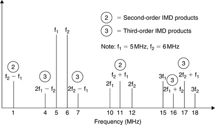
Third-Order Intercept Point (IP3), Second-Order Intercept Point (IP2)
IMD products are of special interest in the RF area, and a major concern in the design of radio receivers. Third-order IMD products can mask out small signals in the presence of larger adjacent ones. Third-order IMD is often specified in terms of the third-order intercept point (IP3) as shown in Figure 1-60.

If the system nonlinearity is approximated by a power series expansion, the second-order IMD amplitudes increase 2 dB for every 1 dB of signal increase. Similarly, the third-order IMD amplitudes increase 3 dB for every 1 dB of signal increase. Once the input reaches a certain level, however, the output signal begins to soft limit, or compress due to things like power supply limits, output drive maximums, and the like. But the second- and third-order intercept lines may be extended to intersect the extension of the output signal line. These intersections are called the second- and third-order intercept points, respectively. The values are usually referenced to the output power of the device expressed in dBm. So, while the IP3 point most often will never be reached in practice, it is still used as a figure of merit in high speed systems.
To determine the IP3 point, two spectrally pure tones are applied to the system. The output signal power of a single tone (in dBm) as well as the relative amplitude of the third-order products (referenced to a single tone) is plotted as a function of input signal power. With a low level (well below clipping) two-tone input signal, and two data points, draw the second- and third-order IMD lines as are shown in Figure 1-60, because one point and a slope determine each straight line. Where they intersect will be the second- and third-order intercept points, respectively.
Figure 1-61 shows the third order intercept value as a function of frequency for a typical VFB amplifier.
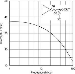
Assume the op amp output signal is 5 MHz and 2 V peak-to-peak into a 100 Ω load (50 Ω source and load termination). The voltage into the 50 Ω load is therefore 1 V peak-to peak, corresponding to +4 dBm. The value of the third-order intercept at 5 MHz is 36 dBm. The difference between +36 dBm and +4 dBm is 32 dB. This value is then multiplied by 2 to yield 64 dB (the value of the third-order intermodulation products referenced to the power in a single tone). Therefore, the intermodulation products should be −64 dBc (dB below carrier frequency), or at a level of −60 dBm. Figure 1-60 shows the graphical analysis for this example.
1 dB Compression Point
Another parameter, which may be of interest, is the 1 dB compression point. This is the point at which the output signal is compressed by 1 dB from the ideal input/output transfer function. This occurs when the dynamic range of the amplifier output is reached and the output will not increase no matter how much the input to the amplifier increases (i.e., clipping). This point is also shown in Figure 1-60.
Signal to Noise Ratio
The SNR is the dynamic range of the system, usually expressed in dB. The reference level is the maximum signal level, and the RMS level of the noise is the floor. The bandwidth of the measurement must be specified.
Equivalent Number of Bits
If we take the SNR of the op amp and express it in bit we have equivalent number of bits (ENOBs). The conversion formula is:
Although we would mainly think of bits in converter applications, they are sometimes used in the context of op amps. Again, the bandwidth of the measurement must be specified.
Spurious Free Dynamic Range
SFDR is another measure of the dynamic range of the system. It can be measured two ways. The first is the difference between the maximum signal and the first distortion component of any type. It would be measured in dB. This would be the SFDR in dBFS. The other way to measure it is in relation to the actual signal strength. This would be the SFDR in dBc (meaning relative to the carrier). While this is again more commonly a converter specification, we sometimes see SFDR used in reference to op amps (Figure 1-62).

Slew Rate
The slew rate of an amplifier is the maximum rate of change of voltage at its output. It is expressed in V/s (or, more probably, V/μs). Op amps may have different slew rates during positive and negative going transitions, due to circuit design, but for this analysis we shall assume that good fast op amps have reasonably symmetrical slew rates.
If we consider a sine wave with a p-p amplitude of 2 Vp and frequency f, the expression for the output voltage is:
One note here, many high speed amplifiers will have overshoot. This means the output will go beyond the final value and will then have a damped oscillation around the final value. This is call “ringing.” The amount of overshoot and ringing will be an indication of the phase margin of the amplifier. The higher the overshoot and the more ringing, the less phase margin.
The slew rate is generally measured between 10% and 90% of the final value (although 20–80% is sometimes also used) (Figure 1-63).

Full Power Bandwidth
The minimum output frequency at which slew limiting occurs is directly proportional to slew rate and inversely proportional to the amplitude of the signal. This allows us to define the “full power bandwidth” (FPBW) of an op amp:
It is important to realize that both slew rate and FPBW can also depend somewhat on the power supply voltage being used and the load the amplifier is driving (particularly capacitive).
In practice, the FPBW of the op amp should be approximately 5–10 times the maximum output frequency in order to achieve acceptable distortion performance (Figure 1-64).
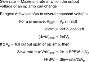
−3 dB Small Signal Bandwidth
The −3 dB bandwidth of an op amp will almost always be greater than the FPBW. This is because the signal does not have to swing as far. Since Vp is reduced, the bandwidth is increased.
Bandwidth for 0.1 dB Flatness
In demanding applications such as professional video, it is desirable to maintain a relatively flat bandwidth and linear phase up to some maximum specified frequency. This is because a change in gain or phase of the system will affect the color intensity or hue.
Simply specifying the 3 dB bandwidth is not enough. It has become customary to specify the 0.1 dB bandwidth, or 0.1 dB bandwidth flatness. This means there is no more than 0.1 dB ripple up to a specified 0.1 dB bandwidth frequency. Video buffer amplifiers generally have both the 3 dB and the 0.1 dB bandwidth specified. Figure 1-65 shows the frequency response of the AD8075 triple video buffer.
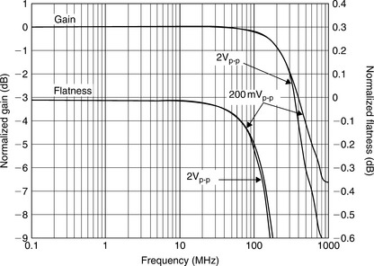
Note that the 3dB bandwidth is approximately 400 MHz. This can be determined from the response labeled “GAIN” in the graph, and the corresponding gain scale is shown on the left-hand vertical axis (at a scaling of 1 dB/division). The response scale for “FLATNESS” is on the right-hand vertical axis, at a scaling of 0.1 dB/division in this case. This allows the 0.1 dB bandwidth to be determined, which is about 65 MHz in this case. The major difference in the applicable bandwidth between 3 and 0.1 dB criteria. It requires a 400 MHz bandwidth amplifier (as conventionally measured) to provide the 65 MHz 0.1 dB flatness rating.
It should be noted that these specifications hold true when driving a 75 Ω source and load terminated cable, which represents a resistive load of 150 Ω. Any capacitive loading at the amplifier output could cause peaking in the frequency response and should be avoided.
Gain-Bandwidth Product
For a VFB amplifier, if the gain at any particular frequency is multiplied by that frequency, the product is a constant. This is because in a first-order system a doubling of frequency causes a reduction in gain by a factor of 2. Therefore this product becomes a useful figure of merit in comparing the bandwidth of op amps (Figure 1-66).
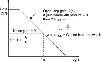
CFB Frequency Dependence
CFB op amps do not behave in the same way as VFB types. They are not stable with capacitive feedback, nor are they so with a short circuit from output to inverting input. With a CFB op amp, there is an optimum feedback resistance for maximum bandwidth. Note that the value of this resistance may vary with supply voltage. If the feedback resistance is increased, the bandwidth is reduced. Conversely, if it is reduced, bandwidth increases, and the amplifier may become unstable (Figure 1-67).

In a CFB op amp, for a given value of feedback resistance, the closed-loop bandwidth is largely unaffected by the noise gain, as shown in Figure 1-67. Thus it is not correct to refer to gain-bandwidth product, for a CFB amplifier, because of the fact that it is not constant. Gain is manipulated in a CFB op amp application by choosing the correct feedback resistor for the device, and then selecting the input resistor to yield the desired closed-loop gain. The signal gain (as determined by the feedback network) of a CFB amplifier is identical to the case of a VFB op amp.
Typically, CFB op amp data sheets will provide a table of recommended resistor values, which provide maximum bandwidth for the device, over a range of gain, supply voltage, and package type. It simplifies the design process considerably to use these tables (see Figure 1-68).

Settling Time
The settling time of an amplifier is defined as the time it takes the output to respond to a step change of input and come within and remain within a defined error band, as measured relative to the 50% point of the input pulse (see Figure 1-69). There is no natural error band for an op amp (a DAC naturally has an error band of 1 LSB, or perhaps ± 1 LSB), so one must be chosen and defined. What is chosen will depend on the performance of the op amp, but since the value chosen will vary from device to device, comparisons are very difficult. This is true because settling is not linear, and many different time constants may be involved. Examples are early op amps using dielectrically isolated (DI) processes. These had very fast settling to 1% of full-scale, but they took almost forever to settle to 10 bits (0.1%). Similarly, some very high precision op amps have thermal effects which cause settling to 0.001% or better to take tens of ms, although they will settle to 0.025% in a few μs.
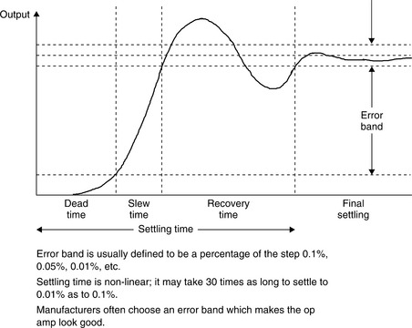
It should also be noted that thermal effects could cause significant differences between short-term settling time (generally measured in nanoseconds) and long-term settling time (generally measured in microseconds or milliseconds). In many AC applications, long-term settling time is not important; but if it is, it must be measured on a much different time scale than short-term settling time.
Rise Time and Fall Time
For high speed op amps we might also have a specification for rise and fall times. While ideally they should be the same, there is typically some difference in practical op amps. Rise and fall times are measured by applying a square wave to the op amp and would be measured on the output waveform. This is closely related to slew rate. Also, as is done with slew rate, we generally measure between the 10% and 90% points, so that overshoot and ringing generally do not enter into the picture. The input wave generally will be full-scale, but occasionally it is specified for a smaller input signal. Overall rise and fall times are a less revealing specification than slew rate and settling time.
Phase Margin
Phase margin is the amount of phase shift when the (VFB) amplifier’s gain passes through 0dB. It is basically a measure of how close the second pole of the system is to causing instability. Phase starts to change on the order of a decade before the corner frequency. The phase shift must be less than 180°. The phase margin is the 180°—the actual phase shift of the amplifier. Anything greater than 45° is usually acceptable. The higher the phase margin, the more stable the system. Capacitive loading will reduce the phase margin.
The graph in Figure 1-70, taken from the data sheet for the AD8054, shows that when the open-loop gain (left scale) falls below 0 dB, the phase margin is around 45° (right scale). This is a respectable value for phase margin. In general, you should avoid phase margins below 20° to 25°.
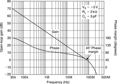
Common-Mode Rejection Ratio
If a signal is applied equally to both inputs of an op amp, so that the differential input voltage is unaffected, the output should not be affected. In practice, changes in common-mode voltage will produce changes in output. The op amp common-mode rejection ratio (CMRR) is the ratio of the common-mode gain to differential-mode gain. For example, if a differential input change of Y volts produces a change of 1 V at the output, and a common-mode change of X volts produces a similar change of 1 V, then the CMRR is X/Y. When the CMRR is expressed in dB, it is generally referred to as common-mode rejection (CMR). Typical low frequency CMR values can be between 70 and 120 dB, but at higher frequencies, CMR deteriorates. In addition to a CMRR numeric specification, many op amp data sheets show a plot of CMR versus frequency, as shown in Figure 1-71 for an OP-177 op amp.

CMRR produces a corresponding output offset voltage error in op amps configured in the non-inverting mode.
Note inverting-mode operating op amps will have less CMRR error. Since both inputs are held at a ground (or virtual ground), there is no common-mode dynamic voltage.
Power Supply Rejection Ratio
If the supply of an op amp changes, its output should not, but it typically does. The specification of power supply rejection ratio or PSRR is defined similarly to the definition of CMRR. If a change of X volts in the supply produces the same output change as a differential input change of Y volts, then the PSRR on that supply is X/Y. The definition of PSRR assumes that both supplies are altered equally in opposite directions; otherwise, the change will introduce a common-mode change as well as a supply change, and the analysis becomes considerably more complex. It is this effect which causes apparent differences in PSRR between the positive and negative supplies (Figure 1-72).
Because op amp PSRR is frequency dependent, op amp power supplies must be well decoupled. At low frequencies, several devices may share a 10–50 μF capacitor on each supply, provided it is no more than 10 cm (PC track distance) from any of them.
At high frequencies, each IC should have the supply leads decoupled by a low inductance 0.1 μF (or so) capacitor with short leads and PC tracks. These capacitors must also provide a return path for high frequency currents in the op amp load. Typical decoupling circuits are shown in Figure 1-73. Further bypassing and decoupling information is found in Chapter 12.
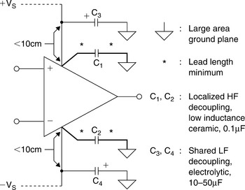
Differential Gain
Differential gain is a specification that originated for video applications. In early video processing equipment it was found that there was sometimes a change in the gain of the amplifier with DC level. More correctly, differential gain is the change in the color saturation level (amplitude of the color modulation) for a change in low frequency luma (brightness) amplitude. This modulation is obviously a distortion, changing the intensity of the color. Professional video editing equipment commonly strives to keep the total differential gain of the system below 1%. Modern high performance video op amps have differential gain specifications of <0.01% (Figures 1-74 to 1-79).


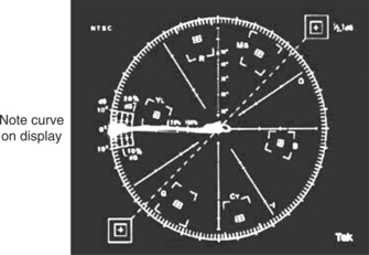
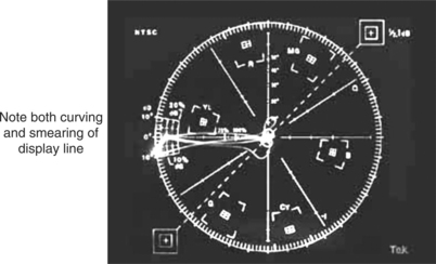
Differential Phase
Differential phase is the change in hue (phase of the color modulation) for a change in low frequency luma (brightness) amplitude. This modulation is obviously a distortion, changing the hue of the color. Professional video editing equipment commonly strives to keep the total differential phase of the system below 1°. Modern, high performance video op amps have differential gain specifications of <0.01°.
Phase Reversal
Phase reversal is a problem that occurs in some op amp when the input common mode of an op amp is exceeded. The mechanism is that one of the internal stages of the op amp no longer has a bias voltage across it and subsequently turns off. The effect is that the output waveform swings to the opposite rail until the input comes back into the common-mode range (see Figure 1-80). This became a big problem with the move toward lower supply voltages and single supplies. Advances in circuit design have resulted in op amps that do not suffer from phase reversal. If the op amp is designed to avoid phase reversal it is generally noted in the bullets or “Key Features” and not necessarily in the specification table.

Channel Separation
Channel separation, otherwise known as crosstalk, is a signal that couples from one amplifier in a package to another amplifier in the same package. The path is typically through the power supply, which will typically be shared between the amplifiers. Careful layout of the op amp chip can minimize the crosstalk. Careful external bypassing of the power supplies can also help.
Absolute Maximum Ratings
The absolute maximum ratings are the voltage, current, and temperature limits of the op amp. Exceeding the absolute maximums can lead to the destruction of the op amp (see Figure 1-81).

Applying overvoltage to input pins is one very common way to destroy an op amp. Overvoltage conditions can be broken into two groups, overvoltage and electrostatic discharge (ESD).
ESD voltages typically run to the thousand of volts. Most of us have experienced ESD. Just shuffle your feet across a nylon carpet, especially in a dry environment, and touch a metal doorknob. Sparks will fly from your fingertips. CMOS circuits are especially prone to ESD.
Overvoltages occur when the maximum voltage allowed on the op amp is exceeded. The maximum allowable voltage is typically set by the supply voltage, although there are a few exceptions. An overvoltage on the inputs will typically cause the input devices to turn into a SCR type structure, usually through the substrate. The failure mechanism is not the overvoltage per se, but instead the current that the overvoltage causes to flow. So if the current is limited, no catastrophic damage will be done. The rule-of-thumb is to limit the current to 5 mA.
While no catastrophic damage will be done, continually overstressing the inputs can cause a change in parameters like bias current and offset voltage. So even though you will not necessarily destroy the amp, overvoltage should be avoided.
Protection for overvoltage can consist of diodes from the input pins to the supplies and current limiting resistors. The diodes are typically Schottky diodes, used because of their lower forward voltage (typically 300 mV versus 700 mV for silicon). Protection devices should be applied with caution though. Some diodes can be leaky, which causes issues similar to those of bias currents. Some can also have fairly high capacitance, which may limit frequency response. This is especially true for high speed amps. Current limiting resistors raise the noise floor. Some op amps, such as the OP-27, include protection diodes, but still require current limiting. If an op amp has protection diodes, it will typically have a specification for maximum differential input current. The protection circuit should also show up on the simplified schematic (Figure 1-82).
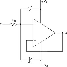
Some op amps also have back to back diodes across the inputs. These are not for input overvoltage protection, but to limit the differential voltage. If these exist, there will be an absolute maximum specification of ±700 mV for the differential input voltage.
The overriding specification for temperature is the maximum junction temperature of 150°C. As this limit is approached, the life expectancy of the amp (actually any semiconductor) goes down (Figure 1-83).
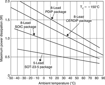
The temperature gradient between the junction and the case is based on the thermal resistance of the package, which is called θJC. There is also a thermal resistance, θCA, from the package to the ambient. These thermal resistances add up linearly, so the total thermal resistance, θJA, from the junction to the ambient is θJC + θCA.
The maximum operation temperature rating has more to do with the temperature performance range of the rest of the specifications of the op amp rather than any potential damage.
References: Op Amp Specifications
1 Ragazzini J.R., Randall R.H., Russell F.A. Analysis of Problems in Dynamics by Electronic Circuits. Proceedings of the IRE. 1947;Vol. 35:444–452. May
2 Borlase W. An Introduction to Operational Amplifiers (Parts 1–3). In: Analog Devices Seminar Notes. Analog Devices, Inc.; 1971.
3 K.D. Swartzel, Jr., “Summing Amplifier,” US Patent 2,401,779, filed, May 1, 1941, issued June 11, 1946.
4 Terman F.E. Feedback Amplifier Design. Electronics. 1937;Vol. 10(1):12–15. January, 50.
5 J.M. West, “Wave Amplifying System,” US Patent 2,196,844, filed, April 26, 1939, issued April 9, 1940.
6 Bode H.W. Relations Between Attenuation and Phase In Feedback Amplifier Design. Bell System Technical Journal. Vol. 19(3), 1940. July. See also: “Amplifier,” US Patent 2,173,178, filed, June 22, 1937, issued July 12, 1938.
7 R. Stata, “Operational Amplifiers—Parts I and II,” Electromechanical Design, September, November 1965.
8 Sheingold D., ed. Applications Manual for Operational Amplifiers for Modeling, Measuring, Manipulating, and Much Else, 2nd Edition, Boston, MA: George A. Philbrick Researchers, Inc., 1965. See also: Applications Manual for Operational Amplifiers for Modeling, Measuring, Manipulating, and Much Else, Philbrick/Nexus Research, Dedham, MA, 1966, 1984.
9 Jung W.G. IC Op Amp Cookbook, 3rd Edition, Prentice-Hall PTR, 1986, 1997. ISBN: 0-13-889601-1.
10 Kester W., ed. Linear Design Seminar. Inc.: Analog Devices, 1995. ISBN: 0-916550-15-X.
11 Franco S. Design with Operational Amplifiers and Analog Integrated Circuits, 2nd Edition, McGraw-Hill, 1998. ISBN: 0-07-021857-9.
12 Video Op Amp. Analog Dialogue. 1990;Vol. 24(3):19.
13 Erdi G. Amplifier Techniques for Combining Low Noise, Precision, and High-Speed Performance. IEEE Journal of Solid-State Circuits. 1981;Vol. SC-16:653–661. December
14 G. Erdi, T. Schwartz, S. Bernardi, and W. Jung, “Op Amps Tackle Noise-and for Once, Noise Loses,” Electronic Design, December, 1980.
15 Erdi G. A Precision Trim Technique for Monolithic Analog Circuits. IEEE Journal of Solid-State Circuits. 1975;Vol. SC-10:412–416. December
16 Wagner R. Laser-Trimming on the Wafer. Analog Dialogue. 1975;Vol. 9(3):3–5.
17 D. Soderquist and G. Erdi, “The OP-07 Ultra-Low Offset Voltage Op Amp,” Precision Monolithics AN-13, December, 1975.
18 W. Kester (Ed.), High Speed Design Techniques, Analog Devices, 1996, ISBN: 0-916550-17-6 (available for download at http://www.analog.com).
19 W. Kester (Ed.), Practical Analog Design Techniques, Analog Devices, 1995, ISBN: 0-916550-16-8 (available for download at http://www.analog.com).
20 W. Palmer and B. Hilton, “A 500 V/µs 12 Bit Transimpedance Amplifier,” ISSCC Digest, February 1987, pp. 176–177, 386.
21 F.E. Terman, “Feedback Amplifier Design,” Electronics, January 1937, pp. 12–15, 50.
22 E.L. Ginzton, “DC Amplifier Design Techniques,” Electronics, March 1944, pp. 98–102.
23 S.E. Miller, “Sensitive DC Amplifier with AC Operation,” Electronics, November 1941, pp. 27–31, 105–109.
24 Edson J.O., Henning H.H. Broadband Codecs for an Experimental 224 Mb/s PCM Terminal. Bell System Technical Journal. 1965;Vol. 44(9):1887–1950. November
25 Op Amps Combine Superb DC Precision and Fast Settling. Analog Dialogue. 1988;Vol. 22(2):12–15.
26 D.A. Nelson, “Settling Time Reduction in Wide-Band Direct-Coupled Transistor Amplifiers,” US Patent 4,502,020, filed, October 26, 1983, issued February 26, 1985.
27 R.A. Gosser, “DC-Coupled Transimpedance Amplifier,” US Patent 4,970,470, filed, October 10, 1989, issued November 13, 1990.
28 Melsa J.L., Schultz D.G. Linear Control Systems. McGraw-Hill, 1969;196–220. ISBN: 0-07-041481-5
29 L. Smith and D. Sheingold, “Noise and Operational Amplifier Circuits,” Analog Dialogue, Vol. 3, No. 1, pp. 1, 5–16. See also: Analog Dialogue 25th Anniversary Issue, pp. 19–31, 1991
30 Frederiksen T.M. Intuitive Operational Amplifiers. McGraw-Hill, 1988. ISBN: 0-07-021966-4.
31 Roberge J.K. Operational Amplifiers-Theory and Practice. John Wiley, 1975. ISBN: 0-471-72585-4.
32 Stout D., Kaufman M. Handbook of Operational Amplifier Circuit Design. New York: McGraw-Hill, 1976. ISBN: 0-07-061797-X.
33 Dostal J. Operational Amplifiers. New York: Elsevier Scientific Publishing, 1981. ISBN: 0-444-99760-1.
34 Gray P.R., Meyer R.G. Analysis and Design of Analog Integrated Circuits, 3rd Edition, John Wiley, 1993. ISBN: 0-471-57495-3.
35 R. Gosser, “Wide-Band Transconductance Generator,” US Patent 5,150,074, filed, May 3, 1991, issued September 22, 1992.
36 R. Gosser, “DC-Coupled Transimpedance Amplifier,” US Patent 4,970,470, filed, October 10, 1989, issued November 13, 1990.
37 Data sheet for AD8011 300 MHz, 1 mA Current Feedback Amplifier, http://www.analog.com.
38 W. Kester (Ed.), Amplifier Applications Guide, Analog Devices, 1992, ISBN: 0-916550-10-9.
39 W. Kester (Ed.), Practical Design Techniques for Sensor Signal Conditioning, Analog Devices, 1999, ISBN: 0-916550-20-6.
40 Data Sheet for AD8551/AD8552/AD8554 Zero-Drift, Single-Supply, Rail-to-Rail Input/Output Operational Amplifiers, http://www.analog.com.
41 Data Sheet for AD8571/AD8572/AD8574 Zero-Drift, Single-Supply, Rail-to-Rail Input/Output Operational Amplifiers, http://www.analog.com.
42 Data Sheet for OP777/OP727/OP747 Precision Micropower Single-Supply Operational Amplifiers, http://www.analog.com.
43 Data Sheet for OP1177/OP2177/OP4177 Precision Low Noise, Low Input Bias Current Operational Amplifiers, http://www.analog.com.
SECTION 1-3 How to Read a Data Sheet
While there is not an industry standard concerning the format of data sheets, what they cover, what information is included and where that information is located, for the most part data sheets from various manufacturers generally are similar in construction. In this section we will take a look at several data sheets and try to give a feel for where to find certain information and how to interpret what is found.
As a demonstration we will look at five data sheets: a precision amp (OP-1177/OP-2177/OP-4177), a single supply amp (AD8531/AD8532/AD8534), a high speed VFB amp (AD8051/AD8052/AD8054), a CFB amp (AD8001), and the AD847. The part numbers chosen are arbitrary; they were chosen only to give a range of parts.
The Front Page
This page is designed to give you the basic information you might need to choose the part. Referring to Figure 1-84, we can break the front page up into three sections.
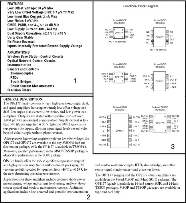
Section 1 is the features. These bullet points are what are considered by the manufacturer to be the more important parameters of the product for its intended application. The targeted applications are typically listed as well.
Section 2 is the product description. This typically covers some of what the manufacturer considers to be the salient features of the op amp.
The third section is the functional block diagram. For an op amp, this is typically the pin out of the various packages. For more complex parts, it will truly be a block diagram.
The Specification Tables
There are an unlimited number of conditions possible when measuring any given specification. Obviously, it is not possible to test all possible conditions. So a representative set of conditions are chosen. The test conditions are specified (1 in Figure 1-85). Occasionally if further clarification of or modification to the conditions is required, it is handled as a footnote (2 in Figure 1-85).

In some cases, when the op amp is specified over a large range of conditions, there may be several specification pages. Each would have a different set of conditions. For instance, an op amp may be specified with a ± 15 V power supply, a ±5 V power supply, or a +5 V only supply. See the AD8051/AD8052/AD8054 data sheet as an example (Figures 1-86 to 1-88).

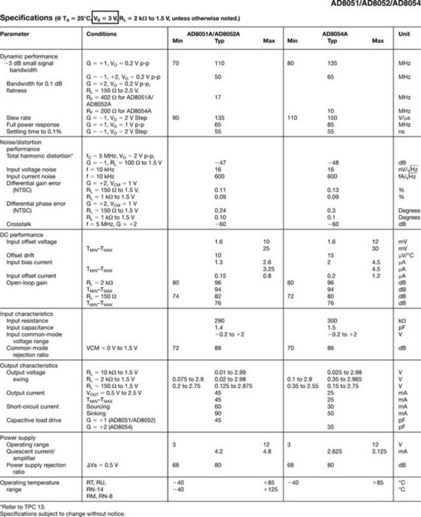

On many op amps some individual specifications may have multiple entries. This is for different performance levels. It can also be for different temperature ranges (usually commercial, industrial, or military). This can be seen in Figure 1-85 (3).
Note that there are typically three possibilities for the specifications, Min, Typ, and Max (see Figure 1-85 (3)). At ADI any specification in the min (minimum) and max (maximum) columns will be guaranteed by test. This can be a direct test, or, in some instances, testing one parameter will guarantee another. A typ (typical) specification is just that, typical. Depending on the particular specification, the deviation from the typical can be substantial. And you have no way of knowing what the range of variation on the typ specification is. Sometimes you will find a typ and a min (or max) for the same specification. This tells you that although the test limits are at a particular level (min or max), the typicals tend to run much better than the test limits. When designing, using typs is risky. You are much better off using mins or maxes for error budget analysis.
Testing is one of the most expensive steps in the manufacturing of op amps. Therefore a more highly specified part will typically cost more than a less completely specified part. But, in your system, the higher specified part may be required to guarantee the circuit performance.
The Absolute Maximums
There is always a section just after the specification tables that contains the absolute maximum ratings. These are typically voltage and temperature related.
The process used to fabricate the op amp will typically determine the maximum supply voltage. Maximum input voltages typically are limited to the supply voltages. It should be pointed out that the supply voltage is the instantaneous value, not the average or final value. So if an op amp has voltages on its input but the supply voltage is not present (which could occur during power up when one section of the system is powered but others are not) the op amp is overvoltaged, even if when the op amp power is applied, everything is within operational limits.
Looking at Figure 1-89, the maximum input voltage specification is GND to VS. The differential input voltage maximum is ±6 V. Note that both of these conditions must be met. So the input pins of the op amp must be between GND and VS and no more than 6 V from each other.

The primary concern for semiconductor reliability is to keep the junction temperature below 150 °C. There will be a θJA given for the various package options. This is the thermal resistance. The units are °C/W (see Figure 1-89). To use this information first determine the power dissipation of the package. This would be the quiescent current times the supply voltage. Then take the maximum dissipation generated by the output stage (output current times the difference between the output voltage and the supply voltage). Add these two together and you will have the total package dissipation, in Watts. Multiply the thermal resistance by the dissipation and you have the temperature rise. Start with the ambient temperature (in °C), take the rise calculated above and that will give you the junction temperature. Remember that the ambient temperature should be in operation. Circuits packaged in an enclosure, which is in turn placed in a rack with other equipment, will have an internal ambient temperature that could be significantly above the air temperature where it is located. This must be considered.
As an example, let us take the AD8534. We will assume that it is being used as a line driver. The required output voltage range is 500 mV to 5 V. The maximum output current we expect from each of the four sections is 100 mA at a maximum output voltage of 5 V. This equates to a load of 50 Ω. Let us say the circuit will operate on a supply of 5.5 V. This allows for a bit of headroom for the driver. If you plot the output voltage versus output current for an amplifier with a resistive load, the maximum dissipation is approximately 55% of the maximum (see Figure 1-90). This is due to the fact that as the output voltage increases, the dissipation voltage (the difference between the output voltage and the supply voltage) decreases, even though the current keeps increasing. Remember it is the power dissipation of the package, not the load, which will rise with increasing output voltage. The quiescent current (Iq) is 1.75 mA maximum over temperature per amplifier. For the four amplifiers, then, the total quiescent dissipation is: 38.5 mW (Iq × VS × 4). The maximum output dissipation is calculated from the following equation:

which calculates to 150 mW per amplifier or 600 mW total. The total dissipation is therefore 638.5 mW.
We chose a TSSOP package because it was the smallest available. The θJA for this package is 240°C/W. This gives a temperature rise of 154°C (240°C/W × 638.5 mW). If the ambient temperature is assumed to be 25°C (the usual value given for room temperature), the junction temperature would be 179°C!!! This is a problem. So we can see that even though we are operating the AD8534 below what would seem to be its maximum output current rating (which is 250 mA), the part will not be reliable since the junction temperature (150°C) will be exceeded.
θJA actually has two components, θJC (the thermal resistance from the junction to the case) and θCA (the thermal resistance from the case to the ambient). They add linearly. We cannot do anything about the θJC, but by adding a heat sink we can change θCA to some degree. Most of the time with op amps, this is not an issue, but it could help for a high current output op amp in a small package as in the example above.
The Ordering Guide
Many op amps are available in multiple packages and/or multiple temperature ranges. Each of the various combinations of package and temperature range requires a unique part number. This is spelled out in the ordering guide (see Figure 1-91.)
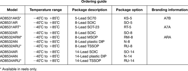
Just as a note, in the case of op amps, the commercial (0°C to 70°C) temperature range has become much less common. The reason for this is that most circuits yield to the industrial temperature range. It is less expensive to support fewer part types. Each discrete part number requires a separate test program, separate inventorying, etc. An exception to this rule is for parts designed for a specific application which is, by definition, commercial. An example of this is consumer applications, such as audio. Wider temperature range for these parts offers no advantage.
The industrial temperature range can also mean different things. The standard industrial temperature range is −40°C to 85°C. A common variant on this is what is commonly called the automotive temperature range, −40°C to 105°C. 0°C to 100°C is also common.
The Graphs
Many specifications vary over the operational range of the op amp. An example is the variation of open-loop gain with frequency (see Figure 1-92). So to completely specify the open-loop gain of a part there would be an open-loop gain specification at DC, which typically would appear in the specification table, and a graph showing variation with frequency. The information presented in the graphs is not uniform from vendor to vendor or even from part to part from the same manufacturer. Higher performance parts tend to be more completely specified. For the most part the graphs will tend to be typical values.

The Main Body
The main body of the data sheet contains detailed information on the operation and applications of the op amp.
The main body typically starts off with a section on the theory of operation of the part. This is usually a short description of the various specifications that are particularly to build was not the best approach. Typically simple calculations—noise, for example—are worked out as examples. The rest of the body of the data sheet contains application information. Since its founding ADI determined that just giving people an amplifier and letting them go off on their own to try to build whatever it is that they want. Therefore, ADI includes application information with the data sheet appropriate for the specific op amp. For instance a precision op amp will emphasize offset and noise, while a high speed op amp will emphasize bandwidth and speed. Much of the information in the applications section is relevant to op amps other than the one that it appears in. The last thing that is typically included in the data sheet is the package drawings (Figure 1-93).

SECTION 1-4 Choosing an Op Amp
As we have seen in the previous sections, an op amp can have many specifications. Now that we have gone over what those specifications mean and how to read a data sheet, we are ready to proceed to the next step. How, then, do you determine which amp best suits your needs?
Step 1: Determine the Parameters
The first step in the process is to determine what parameters are important to your design. To do this you must have a clear idea of:
For instance, if you are designing a single supply system that is going to be capacitively coupled, offsets probably are not a concern. If you are designing a system to interface to a low level physical sensor, then noise, DC precision, and closed-loop gain are important, but bandwidth is probably of less importance, since the bandwidth of most physical sensors is relatively low. However, you do need enough bandwidth to support the required closed-loop gain.
Part of this process is determining the values for the various parameters. In doing this you should determine both an optimum value and an acceptable range. For example, you may have a target value of 500 μV for the offset voltage, but you may be able to live with 1 mV and by relaxing this specification, a better overall fit could be made. The operating temperature range that the circuit will be required to operate in will affect this as well. The physical size of the package and the cost, as always, should be considered. It is also good practice to allow a little margin on the specifications so that aging effects, etc., do not cause the circuit to go out of specification.
Step 2: Prioritize the Parameters
The next step is to prioritize these parameters. Typically one or two parameters are critical. A few more may be desirable but not required. Try not to overspecify the part. Remember that the more specified a part is, the harder it will be to find an exact match; and the tighter the specifications, the more expensive the part is likely to be.
Step 3: Selecting the Part
The next step is to finally select the part. The brute force method would be to gather data sheets and randomly start to look at the specifications for each of the parts individually. This can quickly get out of hand. There are several tools that make the job much easier.
The first is to use selection guides. These appear frequently in magazine ads and promotional mailers. The problem with using these guides is that, in many instances, the lists are not all inclusive, but instead are usually focused on a specific sub group, such as new products, single supply, or the like. The narrow focus may cause you to miss some otherwise acceptable options.
An alternative is a parametric search engine. Here you enter the relevant parameters for your design. The search engine will then search the database of parts and it will come up with acceptable alternatives.