
CHAPTER 6 Converters
![]() Section 6-1: DAC Architectures
Section 6-1: DAC Architectures
![]() Section 6-2: ADC Architectures
Section 6-2: ADC Architectures
![]() Section 6-3: Sigma–Delta Converters
Section 6-3: Sigma–Delta Converters
![]() Section 6-4: Defining the Specifications
Section 6-4: Defining the Specifications
![]() Section 6-5: DAC and ADC Static Transfer Functions and DC Errors
Section 6-5: DAC and ADC Static Transfer Functions and DC Errors
![]() Section 6-6: Data Converter AC Errors
Section 6-6: Data Converter AC Errors
![]() Section 6-7: Timing Specifications
Section 6-7: Timing Specifications
Chapter Introduction
There are two basic types of converters, digital-to-analog (DACs or D/As) and analog-to-digital (ADCs or A/Ds). Their purpose is fairly straightforward. In the case of DACs, they output an analog voltage that is a proportion of a reference voltage, the proportion based on the digital word applied. In the case of ADCs, a digital representation of the analog voltage that is applied to the ADCs input is outputted, the representation proportional to a reference voltage.
In both cases the digital word is almost always based on a binarily weighted proportion. The digital input or output is arranged in words of varying widths, referred to as bits, typically anywhere from 6 bits to 24 bits. In a binarily weighted system each bit is worth half of the bit to its left and twice the bit to its right. The greater the number of bits in the digital word, the finer the resolution. These bits are typically arranged in groups of 4, called bytes, for convenience.
For a better understanding of the relationship between the digital domain and the analog domain please refer to the section on sampling theory.
As stated earlier, we shall look at the operation of converters primarily from a “black box” view. We will concern ourselves less with the internal construction of the converter and more with its operation. We cannot, however, completely ignore the internal architecture because in many cases it is relevant to operational advantages or limitations. There are a number of works that cover the internal workings of the converters in much more detail (see references).
Another point that should be kept in mind is the difference between accuracy and resolution. The resolution of a converter is the number of bits in its digital word. The accuracy is the number of those bits that meet the specifications. For instance, a DAC might have 16 bits of resolution, but might only be monotonic to 14 bits. This means that the assured accuracy of the DAC will be no better than 14 bits. Also, an audio ADC might have a digital word width of 16 bits, but the signal-to-noise ratio (SNR) may be only 70 dB. This means that the accuracy will only be at the 12-bit level. This is not to say that the other bits are irrelevant. With further processing, typically filtering, often the accuracy can be improved. While these terms are similar and sometimes used interchangeably, the distinction between the two should be remembered.
SECTION 6-1 DAC Architectures
DACs or D/As Introduction
What we commonly refer to as a DAC today is typically quite a bit more. The DAC will typically have the converter itself and a collection of support circuitry built into the chip (Figure 6-1).

The first DACs were board level designs, built from discrete components, including vacuum tubes as the switching elements. Monolithic DACs began to appear in the early 1970s. These early examples were actually sub-blocks of the DAC. An example of this would be the AD550, which was a 4 bit binarily weighted current source. This current source block would be mated to a separate part, such as the AD850, which contained a resistor array and complementary-MOS (CMOS) switches. Together these would form the basic DAC. As we moved on in time these functions were integrated on the same die, additional digital circuitry, specifically latches to store the digital input, were added. Then a second rank of latches were often added. The purpose of the second rank was to allow the microprocessor or microcontroller to write many DACs in a system and update them all at the same time. The input rank of latches could also be a shift register, which would allow a serial interface.
On the back end, since the output of the DAC is often a current, an op amp is often added to perform the current-to-voltage (I/V) conversion. On the front end a voltage reference is often added.
Process limitations did not allow the integration of all these sub-blocks to occur at once. Initially, the processes used to make the various sub-blocks were not compatible. The process that made the best switches was typically not the best for the amplifier and the reference. As the processes became more advanced these limitations became less. Today CMOS can make acceptable amplifiers and processes combining bipolar and CMOS together exist.
There are several advantages to including all this additional circuitry in one package. The first is the obvious advantage of reducing the chip count. This reduces the size of the circuitry and increases the reliability. Probably more important is that the circuit designer now does not have to concern himself with the accuracy of several parts in a system. The system is now one part and tested by the manufacturer as a unit.
Next we will look at the various DAC architectures. When we refer to DACs here we are referring to the basic converter rather than the complete system.
Kelvin Divider (String DAC)
The simplest structure of all is the Kelvin divider or string DAC as shown in Figure 6-2. An N-bit version of this DAC simply consists of 2N equal resistors in series and 2N switches (usually CMOS), one between each node of the chain and the output. The output is taken from the appropriate tap by closing just one of the switches (there is some slight digital complexity involved in decoding to 1 of 2N switches from N-bit data).

This architecture is simple, has a voltage output, and is inherently monotonic—even if a resistor is accidentally short-circuited, output n cannot exceed output n + 1. It is linear if all the resistors are equal, but may be made deliberately nonlinear if a nonlinear DAC is required. The output is a voltage, but it has the disadvantage of having a relatively large output impedance. This output impedance is also code dependent (the impedance changes with changes to the digital input). In many cases it will be beneficial to follow the output of the DAC with an op amp to buffer this output impedance and present a low impedance source to the following circuitry.
Since only two switches operate during a transition it is a low glitch architecture (the concept of glitch will be examined in a following section). Also, the switching glitch is not code-dependent, making it ideal for low distortion applications. Because the glitch is constant regardless of the code transition, the frequency content of the glitch is at the DAC update rate and its harmonics—not at the harmonics of the DAC output signal frequency. The major drawback of the Kelvin DAC is the large number of resistors and switches required for high resolution. There are 2N resistors required, so a 10-bit DAC would require 1,024 switches and resistors, and as a result it was not commonly used as a simple DAC architecture until the recent advent of very small integrated circuit (IC) feature sizes made it very practical for low and medium resolution (typically up to 10 bits) DACs.
As we mentioned in the section on sampling theory, the output of a DAC for an all 1s code is 1 least significant bit (LSB) below the reference, so a Kelvin divider DAC intended for use as a general purpose DAC has a resistor between the reference terminal and the first switch as shown in Figure 6-2.
Segmented String DACs
A variation of the Kelvin divider is the segmented string DAC. Here we reduce the number of resistors required by segmenting. Figure 6-3 shows two varieties of segmented voltage-output DAC. The architecture in Figure 6-3(A) is sometimes called a Kelvin–Varley divider. Since there are buffers between the first and second stages, the second string DAC does not load the first, and the resistors in the second string do not need to have the same value as the resistors in the first. All the resistors in each string, however, do need to be equal to each other or the DAC will not be linear. The examples shown have 3-bit first and second stages but for the sake of generality, let us refer to the first (most significant bit (MSB)) stage resolution as M bits and the second (LSB) as K bits for a total of N = M + K bits. The MSB DAC has a string of 2M equal resistors, and a string of 2K equal resistors in the LSB DAC. As an example if we make a 10-bit string DAC out of two 5-bit sections, each segment would have 25 or 32 resistors, for a total of 64, as opposed to the 1,024 required for a standard Kelvin divider. This is an obvious advantage.

Buffer amplifiers can have offset, of course, and this can cause non-monotonicity in a buffered segmented string DAC.
In the simpler configuration of a buffered Kelvin–Varley divider buffer (Figure 6-3(A)), buffer A is always “below” (at a lower potential than) buffer B, and the extra tap labeled “A” on the LSB string DAC is not necessary. The data decoding is just two priority encoders.
But if the decoding of the MSB string DAC is made more complex so that buffer A can only be connected to the taps labeled “A” in the MSB string DAC, and buffer B to the taps labeled “B,” then it is not possible for buffer offsets to cause non-monotonicity. Of course, the LSB string DAC decoding must change direction each time one buffer “leapfrogs” the other, and taps A and B on the LSB string DAC are alternately not used—but this involves a fairly trivial increase in logic complexity and is justified by the increased performance.
Rather than using a second string of resistors, a binary R–2R DAC can be used to generate the three LSBs as shown in Figure 6-3(B). This voltage-output DAC (Figure 6-3(B)) consists of a 3-bit string DAC followed by a 3-bit buffered voltage-mode ladder network. Again the number of resistors required for the DAC is reduced.
An unbuffered version of the segmented string DAC is shown in Figure 6-4. This version is more clever in concept. Here, the resistors in the two strings must be equal, except that the top resistor in the MSB string must be smaller—1/(2K) of the value of the others—and the LSB string has 2K −1 resistors rather than 2K. Because there are no buffers, the LSB string appears in parallel with the resistor in the MSB string that is switched across and loads it. This drops the voltage across that MSB resistor by 1 LSB of the LSB DAC—which is exactly what is required. The output impedance of this DAC, being unbuffered, varies with changing digital code. This circuit is intrinsically monotonic since it is unbuffered (and, of course, can be manufactured on CMOS processes which make resistors and switches but not high precision amplifiers, so it may be cheaper as well).

In order to understand this clever concept better, the actual voltages at each of the taps has been worked out and labeled for the 6-bit segmented DAC composed of two 3-bit string DACs shown in Figure 6-4. The reader is urged to go through this simple analysis with the second string DAC connected across any other resistor in the first string DAC and verify the numbers. A detailed mathematical analysis of the unbuffered segmented string DAC can be found in the relevant patent filed by Dennis Dempsey and Christopher Gorman of Analog Devices in 1997 (Reference 14).
Digital Pots
Another variation of the string DAC is the digital potentiometer. A simple digital potentiometer is shown in Figure 6-5.

The major difference is that the lower arm of the pot (terminal B) is not connected to ground, but is instead left floating. The absolute values of the resistors in a Kelvin DAC typically are not critical. They are limited by the available material. They must, of course, be the same as each other. In a digital pot the end-to-end resistance is specified. The accuracy of the end-to-end resistance is on the order of a mechanical pot.
Digital pots are typically available in end-to-end resistance values from 10 kΩ to 1 MΩ. Lower values of end-to-end resistance are difficult since the on-resistance of the CMOS switches is on the order of the resistor segment, so the linearity of the pot suffers at the low end.
The advantages to digital pots are many. Even the lowest resolution digital pots have better setability than their mechanical counterparts. Also they are immune to mechanical vibration and oxidation of the wiper contact. Obviously, adjustments can be made without human intervention.
In most digital pots the voltage on the input pins cannot exceed the supplies (typically 3 V or 5 V) due to the CMOS switches used in their construction, but certain models are designed for ± 15 V operation.
Another design feature on many of the digital pots is that on power-up (sometimes from an internal timer, sometimes controlled by an external pin) the wiper is shorted to one of the terminals. This is useful since output on power-up is undefined until it is written to. Since it might take a while (relatively) for the microcontroller to initialize itself and then get around to initializing the rest of the system, having the digital pot in a known state can be useful. Some digital potentiometers incorporate non-volatile logic so that their settings are retained when they are turned off.
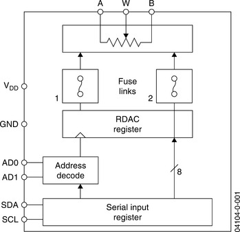
One time programmable (OTP) versions of digital pots have become available. Here the digital code is locked into the pot once the setting had been determined. The technology used is fusible links. A variation on this theme is the two times programmable (TTP) digital pot. This allows the non-volatile settings to be modified one time. The block diagram of a TTP digital pot is shown in Figure 6-6.
Thermometer (Fully Decoded) DACs
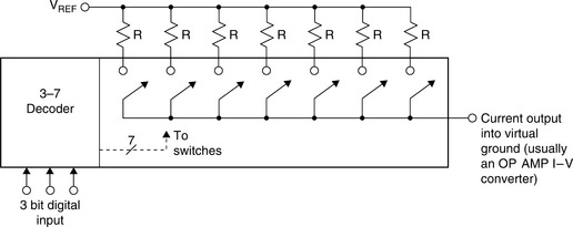
There is a current-output DAC architecture analogous to a string DAC which consists of 2N–1 switchable current sources (which may be resistors and a voltage reference or may be active current sources) connected to an output terminal. This output must be at, or close to, ground. Figure 6-7 shows a thermometer DAC which uses resistors connected to a reference voltage to generate the currents.
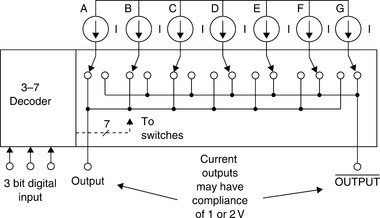
If active current sources are used as shown in Figure 6-8, the output may have more compliance (the allowable voltage on the output pin which still guarantees performance), and a resistive load is typically used to develop an output voltage. The load resistor must be chosen so that at maximum output current the output terminal remains within its rated compliance voltage.

Once a current in a thermometer DAC is switched into the circuit by increasing the digital code, any further increases do not switch it out again. The structure is thus inherently monotonic, irrespective of inaccuracies in the currents. Again, like the Kelvin divider, only the advent of high density IC processes has made this architecture practical for general purpose medium resolution DACs, although a slightly more complex version—shown in the next diagram—is quite widely used in high speed applications. Unlike the Kelvin divider, this type of current-mode DAC does not have a unique name, although both types may be referred to as fully decoded DACs or thermometer DACs.
A DAC where the currents are switched between two output lines—one of which is often grounded, but may, in the more general case, be used as the inverted output—is more suitable for high speed applications because switching a current between two outputs is far less disruptive, and so causes a far lower glitch than simply switching a current on and off. This architecture is shown in Figure 6-9.
But the settling time of this DAC still varies with initial and final code, giving rise to intersymbol distortion (ISI). This can be addressed with even more complex switching where the output current is returned to zero before going to its next value. Note that although the current in the output is returned to zero it is not “turned off”—the current is dumped to ground when it is not being used, rather than being switched on and off. The techniques involved are too complex to discuss in detail here but can be found in the references.
In the normal (linear) version of this DAC, all the currents are nominally equal. Where it is used for high speed reconstruction, its linearity can also be improved by dynamically changing the order in which the currents are switched by ascending code. Instead of code 001 always turning on current A; code 010 always turning on currents A and B; code 011 always turning on currents A, B, and C; etc. the order of turn-on relative to ascending code changes for each new data point. This can be done quite easily with a little extra logic in the decoder. The simplest way of achieving it is with a counter which increments with each clock cycle so that the order advances: ABCDEFG, BCDEFGA, CDEFGAB, etc. but this algorithm may give rise to spurious tones in the DAC output. A better approach is to set a new pseudo-random order on each clock cycle—this requires a little more logic, but even complex logic is now very cheap and easily implemented on CMOS processes. There are other, even more complex, techniques which involve using the data itself to select bits and thus turn current mismatch into shaped noise. Again they are too complex for a book of this sort (see references for a more detailed discussion).
Binary-Weighted Current Source
The voltage-mode binary-weighted resistor DAC shown in Figure 6-10 is usually the simplest textbook example of a DAC. However, this DAC is not inherently monotonic and is actually quite hard to manufacture successfully at high resolutions due to the large spread in component (resistor) values. In addition, the output impedance of the voltage-mode binary DAC changes with the input code.

Current-mode binary-weighted DACs are shown in Figure 6-11(A) (resistor-based), and Figure 6-11(B) (current-source based). An N-bit DAC of this type consists of N-weighted current sources (which may simply be resistors and a voltage reference) in the ratio 1:2:4:8: …:2N–1. The LSB switches the 2N–1 current, the MSB the 1 current, etc. The theory is simple but the practical problems of manufacturing an IC of an economical size with current or resistor ratios of even 128:1 for an 8-bit DAC are enormous, especially as they must have matched temperature coefficients. This architecture is virtually never used on its own in IC DACs, although, again, 3- or 4-bit versions have been used as components in more complex structures. For example, the AD550 mentioned at the beginning of this section is an example of a binary-weighted DAC.

If the MSB current is slightly low in value, it will be less than the sum of the other bit currents, and the DAC will not be monotonic (the differential nonlinearity (DNL) of most types of DAC is worst at major bit transitions).
However, there is another binary-weighted DAC structure which has recently become widely used. This uses binary-weighted capacitors as shown in Figure 6-12. The problem with a DAC using capacitors is that leakage causes it to lose its accuracy within a few milliseconds of being set. This may make capacitive DACs unsuitable for general purpose DAC applications, but it is not a problem in successive approximation ADCs, since the conversion is complete in a few microseconds or less—long before leakage has any appreciable effect.
The use of capacitive charge redistribution DACs offers another advantage as well—the DAC itself behaves as a sample-and-hold amplifier (SHA) circuit, so not only is an external SHA unnecessary with these ADCs, there is no need to allocate separate chip area for a separate integral SHA.
R–2R Ladder
One of the most common DAC building-block structures is the R–2R resistor ladder network shown in Figure 6-13. It uses resistors of only two different values, and their ratio is 2:1. An N-bit DAC requires 2 N resistors, and they are quite easily trimmed. There are also relatively few resistors to trim.

This structure is the basis of a large family of DACs. Figure 6-14 is the block diagram of the AD7524, which is typical of a basic current-output CMOS DAC. The diagram shows the structure of the DAC.

The input impedance (basically the value of the resistors) is not a closely specified parameter. The specified range is 4:1 (5 kΩ minimum, 20 kΩ maximum, although it is typically closer than that). It is the relative accuracy, not the absolute accuracy of the resistors that is of interest. In most applications the absolute value is not important. Certain applications exist where the value does matter. In these instances, the parts must be selected at test.
Note the extra resistor added at the RFEEDBACK pin. This is designed to be the feedback resistor for the I/V op amp. This resistor is trimmed along with the rest of the resistors so it tracks. Also, since it is made of the same material as the rest of the resistors, therefore having the same temperature coefficient, and is on the same substrate, hence at the same temperature, it will track over temperature.
Figure 6-15 shows a more modern example of a CMOS DAC, the AD7394. Several trends are obvious here. First off all, the output is voltage, not current. Advancements in process technology have allowed reasonable quality CMOS op amps to be created. Also note the two ranks of latches. The purpose of these latches is to allow the microcontroller to write to all converters in a system and then update them all at the same time. This will be covered in more detail in a later section. Note also the power on reset circuit. Since the wake up state of a CMOS DAC is undefined and not repeatable, many modern DACs include a circuit to force the output to either half-scale of minimum scale, depending on whether the intended application is unipolar or bipolar. Probably the most obvious difference is that this is a multiple DAC package. Shrinking device geometries have allowed more circuitry to be included, even with the smaller packages in use today.

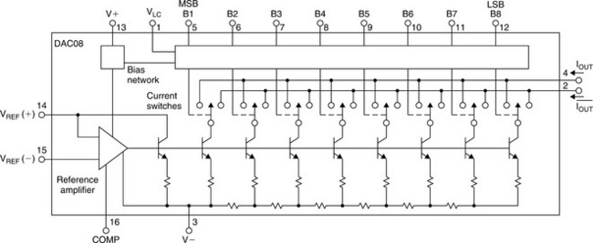
The previous examples were CMOS devices, that is to say that the switches were implemented with CMOS switches. The switches could also be implemented with bipolar junction transistors (BJT). An example of this is the classic DAC-08. Its block diagram is shown in Figure 6-16. One major difference in the BJT implementation is that the switch allows current in one direction, versus the CMOS switch, which can allow bidirectional current. This limits the BJT DAC to two-quadrant operation while the CMOS version can be four-quadrant. Supplies tend to be different as well.
There are two ways in which the R–2R ladder network may be used as a DAC—known respectively as the voltage mode and the current mode (they are sometimes called “normal” mode and “inverted” mode, but as there is no consensus on whether the voltage mode or the current mode is the “normal” mode for a ladder network this nomenclature can be misleading, although in most cases the current mode would be considered the “normal” mode). Each mode has its advantages and disadvantages.
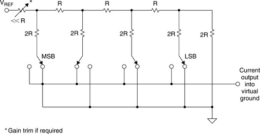
In the current-mode R–2R ladder DAC shown in Figure 6-17, the gain of the DAC may be adjusted with a series resistor at the VREF terminal, since in the current mode, the end of the ladder, with its code-independent impedance, is used as the VREF terminal; and the ends of the arms are switched between ground and an output line which must be held at ground potential. The normal connection of a current-mode ladder network output is to an op amp’s inverting input (virtual ground), but stabilization of this op amp is complicated by the DAC output impedance variation with digital code.
Current-mode operation has a larger switching glitch than voltage mode since the switches connect directly to the output line(s). However, since the switches of a current-mode ladder network are always at ground potential, their design is less demanding and, in particular, their voltage rating does not affect the reference voltage rating. If switches capable of carrying current in either direction (such as CMOS devices) are used, the reference voltage may have either polarity, or may even be AC. Such a structure is one of the most common types used as a multiplying DAC (MDAC) which will be discussed later in this section.
Since the switches are always at, or very close to, ground potential, the maximum reference voltage may greatly exceed the logic voltage, provided the switches are make-before-break—which they are in this type of DAC. It is not unknown for a CMOS MDAC to accept a ± 30 V reference (or even a 60 V peak-to-peak AC reference) while working from a single 5 V supply.
In the voltage-mode R–2R ladder DAC shown in Figure 6-18, the “rungs” or arms of the ladder are switched between VREF and ground, and the output is taken from the end of the ladder. The output may be taken as a voltage, but the output impedance is independent of code, so it may equally well be taken as a current into a virtual ground.

The voltage output is an advantage of this mode, as is the constant output impedance, which eases the stabilization of any amplifier connected to the output node. Additionally, the switches switch the arms of the ladder between a low impedance VREF connection and ground, which is also, of course, low impedance, so capacitive glitch currents tend not to flow in the load. On the other hand, the switches must operate over a wide voltage range (VREF to ground), which is difficult from a design and manufacturing viewpoint, and the reference input impedance varies widely with code, so that the reference input must be driven from a very low impedance. In addition, the gain of the DAC cannot be adjusted by means of a resistor in series with the VREF terminal. Probably the most important advantage to the voltage mode is that it allows single-supply operation. This is because the op amp that is commonly used as I/V converter in the current-mode converter is in the inverting configuration so would require a negative output for a positive input, assuming ground reference. Of course you could bias everything up to a rail-splitter ground, but that introduces other issues into the system.
Multiplying DACs
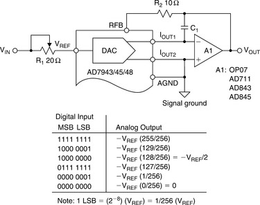
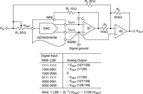
In most cases the reference to a DAC is a highly stable DC voltage. In some instances, however, it is useful to have a variable reference. The R–2R ladder structure using CMOS switches can easily handle a bipolar signal on its input. Having the ability to have bipolar (positive and negative) signals on the input allows construction of two-quadrant and four-quadrant MDACs. Figure 6-19 shows the schematic and the table in this figure outlines the operation of a two-quadrant MDAC, and Figure 6-20 shows the schematic and the table in this figure outlines the operation of a four-quadrant MDAC for an 8-bit DAC.
DACs utilizing BJTs as switches, such as the DAC-08 above, cannot accommodate bipolar signals on the reference. Therefore they can only implement two-quadrant MDACs. In addition, the reference voltage cannot go all the way to 0 V. The maximum allowable range is typically from 10% to 100% of the allowable reference voltage range.
One of the main applications of the MDAC is as a variable gain amplifier, where the gain is controlled by the digital word applied to the MDAC.
The frequency response of the MDAC is limited by the parasitic capacitance across the switches in the off condition. As the frequency goes up the impedance of the capacitors goes down, effectively bypassing the switch. This reduces the off isolation at higher frequencies. Typically the frequency response of an MDAC will be on the order of 1 MHz.
Segmented DACs
So far we have considered mostly basic DAC architectures. When we are required to design a DAC with a specific performance, it may well be that no single architecture is ideal. In such cases, two or more DACs may be combined in a single higher resolution DAC to give the required performance. These DACs may be of the same type or of different types and need not each have the same resolution. For example, the segmented string DAC is a segmented DAC where 2 Kelvin DACs are cascaded.
Typically, one DAC handles the MSBs, another handles the LSBs, and their outputs are added in some way. The process is known as “segmentation,” and these more complex structures are called “segmented DACs.” There are many different types of segmented DACs and some, but by no means all, of them will be illustrated in the next few diagrams. It is sometimes not obvious from looking at the data sheet that a particular DAC is segmented.
Very high speed DACs for video, communications, and other high frequency reconstruction applications are often built with arrays of fully decoded current sources. The 2 or 3 LSBs may use binary-weighted current sources. It is extremely important that such DACs have low distortion at high frequency, and there are several important issues to be considered in their design.
Two examples of segmented current-output DAC structures are shown in Figure 6-21. Figure 6-21(A) shows a resistor-based approach for the 7-bit DAC where the 3 MSBs are fully decoded, and the 4 LSBs are derived from an R–2R network. Figure 6-21(B) shows a similar implementation using current sources. The current source implementation is by far the most popular for today’s high speed reconstruction DACs.

It is also often desirable to utilize more than one fully decoded thermometer section to make up the total DAC. Figure 6-22 shows a 6-bit DAC constructed from two fully decoded 3-bit DACs. As previously discussed, these current switches must be driven simultaneously from parallel latches in order to minimize the output glitch.

The AD9775 14-bit, 160 MSPS (input)/400 MSPS (output) TxDAC™ uses three sections of segmentation as shown in Figure 6-23. Other members of the AD977x-family and the AD985x-family also use this same basic core.

The first 5 bits (MSBs) are fully decoded and drive 31 equally weighted current switches, each supplying 512 LSBs of current. The next 4 bits are decoded into 15 lines which drive 15 current switches, each supplying 32 LSBs of current. The 5 LSBs are latched and drive a traditional binary-weighted DAC which supplies 1 LSB per output level. A total of 51 current switches and latches are required to implement this ultra low glitch architecture.
Decoding must be done before the new data is applied to the DAC so that all the data is ready and can be applied simultaneously to all the switches in the DAC. This is generally implemented by using a separate parallel latch for the individual switches in fully decoded array. If all switches were to change state instantaneously and simultaneously there would be no skew glitch—by very careful design of propagation delays around the chip and time constants of switch resistance and stray capacitance the update synchronization can be made very good, and hence the glitch-related distortion is very small.
I/V Converters
Modern IC DACs provide either voltage or current outputs. Figure 6-24 below shows three fundamental configurations, all with the objective of using an op amp for a buffered output voltage.
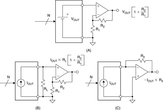
Figure 6-24(A) shows a buffered voltage-output DAC. In many cases, the DAC output can be used directly, without additional buffering. If an additional op amp is needed, it is usually configured in a non-inverting mode, with gain determined by R1 and R2.
There are two basic methods for dealing with a current-output DAC.
A direct method to convert the output current into a voltage is shown in Figure 6-24(C). This circuit is usually called a current-to-voltage converter, or I/V. In this circuit, the DAC output drives the inverting input of an op amp, with the output voltage developed across the R2 feedback resistor. In this approach the DAC output always operates at virtual ground (which may give a linearity improvement vis-à-vis Figure. 6-24(B)).
In Figure 6-24(B) a voltage is simply developed across external load resistor, RL. This is typically done with high speed op amps. An external op amp can be used to buffer and/or amplify this voltage if required. The output current is dumped into a resistor instead of into an op amp directly since the fast edges may exceed the slew rate of the amplifier and cause distortion. Many DACs supply full-scale currents of 20 mA or more, thereby allowing reasonable voltages to be developed across fairly low value load resistors. For instance, fast settling video DACs typically supply nearly 30 mA full-scale current, allowing 1 V to be developed across a source and load terminated 75 Ω coaxial cable (representing a DC load of 37.5 Ω to the DAC output).
The general selection process for an op amp used as a DAC buffer is that the performance of the op amp should not compromise the performance of the DAC. The basic specifications of interest are DC accuracy, noise, settling time, bandwidth, distortion, etc.
Differential to Single-Ended Conversion Techniques
A general model of a modern current-output DAC is shown in Figure 6-25. This model is typical of the AD976X and AD977X TxDAC™ series (see Reference 1).

Current output is more popular than voltage output, especially at audio frequencies and above. If the DAC is fabricated on a bipolar or BiCMOS process, it is likely that the output will sink current, and that the output impedance will be less than 500 Ω (due to the internal R–2R resistive ladder network). On the other hand, a CMOS DAC is more likely to source output current and have a high output impedance, typically greater than 100 kΩ.
Another consideration is the output compliance voltage—the maximum voltage swing allowed at the output in order for the DAC to maintain its linearity. This voltage is typically 1–1.5 V, but will vary depending on the DAC. Best DAC linearity is generally achieved when driving a virtual ground, such as an op amp I/V converter. Modern current-output DACs usually have differential outputs, to achieve high CM rejection and reduce the even-order distortion products. Full-scale output currents in the range of 2–20 mA are common.
In most applications, it is desirable to convert the differential output of the DAC into a single-ended signal, suitable for driving a coax line. This can be readily achieved with a radio frequency (RF) transformer, provided low frequency response is not required. Figure 6-26 shows a typical example of this approach. The high impedance current-output of the DAC is terminated differentially with 50 Ω, which defines the source impedance to the transformer as 50 Ω.
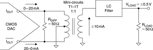
The resulting differential voltage drives the primary of a 1:1 RF transformer, to develop a single-ended voltage at the output of the secondary winding. The output of the 50 Ω LC filter is matched with the 50 Ω load resistor RL, and a final output voltage of 1 Vp-p is developed.
The transformer not only serves to convert the differential output into a single-ended signal, but it also isolates the output of the DAC from the reactive load presented by the LC filter, thereby improving overall distortion performance.
An op amp connected as a differential to single-ended converter can be used to obtain a single-ended output when frequency response to DC is required. In Figure 6-28 the AD8055 op amp is used to achieve high bandwidth and low distortion (see Reference 2). The current-output DAC drives balanced 25 Ω resistive loads, thereby developing an out of phase voltage of 0 V to +0.5 V at each output. The AD8055 is configured for a gain of 8, to develop a final single-ended ground-referenced output voltage of 2 Vp-p. Note that because the output signal swings above and below ground, a dual-supply op amp is required (Figure 6-27).

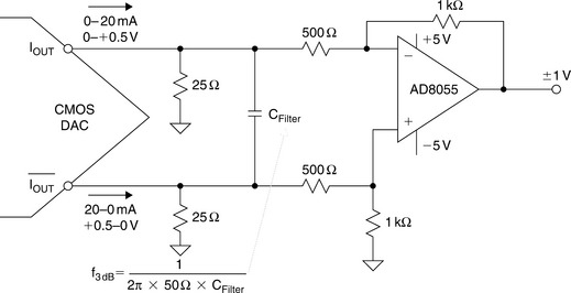
The CFILTER capacitor forms a differential filter with the equivalent 50 Ω differential output impedance. This filter reduces any slew induced distortion of the op amp, and the optimum cutoff frequency of the filter is determined empirically to give the best overall distortion performance.
A modified form of Figure 6-26 circuit can also be operated on a single supply, provided the CM voltage of the op amp is set to mid-supply (+2.5 V). This is shown in Figure 6-28. The output voltage is 2 Vp-p centered around a CM voltage of +2.5 V. This CM voltage can be either developed from the + 5 V supply using a resistor divider, or directly from a +2.5 V voltage reference. If the +5 V supply is used as the CM voltage, it must be heavily decoupled to prevent supply noise from being amplified.
Single-Ended Current-to-Voltage Conversion
Single-ended current-to-voltage conversion is easily performed using a single op amp as an I/V converter, as shown in Figure 6-29. The 10 mA full-scale DAC current from the AD768 (see Reference 3) develops a 0 V to +2 V output voltage across the 200 Ω RF.
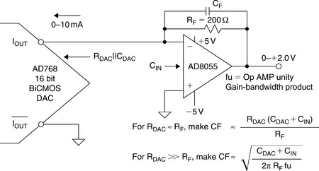
Driving the virtual ground of the AD8055 op amp minimizes any distortion due to nonlinearity in the DAC output impedance. In fact, most high resolution DACs of this type are factory trimmed using an I/V converter.
It should be recalled, however, that using the single-ended output of the DAC in this manner will cause degradation in the CM rejection and increased second-order distortion products, compared to a differential operating mode.
The CF feedback capacitor should be optimized for best pulse response in the circuit. The equations given in the diagram should only be used as guidelines. A more detailed analysis of this circuit is given in the References.
Differential Current-to-Differential Voltage Conversion
If a buffered differential voltage output is required from a current-output DAC, the AD813X-series of differential amplifiers can be used as shown in Figure 6-30.

The DAC output current is first converted into a voltage that is developed across the 25 Ω resistors. The voltage is amplified by a factor of five using the AD813X. This technique is used in lieu of a direct I/V conversion to prevent fast slewing DAC currents from overloading the amplifier and introducing distortion. Care must be taken so that the DAC output voltage is within its compliance rating.
The VOCM input on the AD813X can be used to set a final output CM voltage within the range of the AD813X. If transmission lines are to be driven at the output, adding a pair of 75 Ω resistors will allow this.
Digital Interfaces
The earliest monolithic DACs contained little, if any, logic circuitry, and parallel data had to be maintained on the digital input to maintain the digital output. Today almost all DACs are latched and data need only be written to them, not maintained. Some even have nonvolatile latches and remember settings while turned off.
There are innumerable variations of DAC digital input structure, which will not be discussed here, but nearly all are described as “double-buffered.” A double-buffered DAC has two sets of latches. Data is initially latched in the first rank and subsequently transferred to the second as shown in Figure 6-31. There are two reasons why this arrangement is useful.

The first is that it allows data to enter the DAC in many different ways. A DAC without a latch, or with a single latch, must be loaded in parallel with all bits at once, since otherwise its output during loading may be totally different from what it was or what it is to become. A double-buffered DAC, on the other hand, may be loaded with parallel data, or with serial data, or with 4-bit or 8-bit words, or whatever, and the output will be unaffected until the new data is completely loaded and the DAC receives its update instruction.
The other convenience of the double-buffered structure is that many DACs may be updated simultaneously: data is loaded into the first rank of each DAC in turn, and when all is ready, the output buffers of all the DACs are updated at once. There are many DAC applications where the output of a number of DACs must change simultaneously, and the double-buffered structure allows this to be done very easily.
Most early monolithic high resolution DACs had parallel or byte-wide data ports and tended to be connected to parallel data buses and address decoders and addressed by microprocessors as if they were very small write-only memories. (Some parallel DACs are not write-only, but can have their contents read as well—this is convenient for some applications, but is not very common.) A DAC connected to a data bus is vulnerable to capacitive coupling of logic noise from the bus to the analog output. Serial interfaces are less vulnerable to such noise (since fewer noisy pins are involved), use fewer pins and therefore take less board space, and are frequently more convenient for use with modern microprocessors, most of which have serial data ports. Some, but not all, of such serial DACs have data outputs as well as data inputs so that several DACs may be connected in series and data clocked to them all from a single serial port. This arrangement is often referred to as “daisy-chaining.”
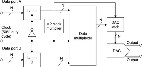
Of course, serial DACs cannot be used where high update rates are involved, since the clock rate of the serial data would be too high. Some very high speed DACs actually have two parallel data ports and use them alternately in a multiplexed fashion (sometimes this is called a “ping-pong” input) to reduce the data rate on each port as shown in Figure 6-32. The alternate loading (ping-pong) DAC in the diagram loads from port A and port B alternately on the rising and falling edges of the clock, which must have a mark-space ratio close to 50:50. The internal clock multiplier ensures that the DAC itself is updated with data A and data B alternately at exactly 50:50 time ratio, even if the external clock is not so precise.
Historically IC logic circuitry (with the exception of emitter coupled logic or ECL) operated from 5 V supplies and had compatible logic levels—with a few exceptions 5 V logic would interface with other 5 V logic. Today, with the advent of low voltage logic operating with supplies of 3.3 V, 2.7 V or even less, it is important to ensure that logic interfaces are compatible. There are several issues which must be considered—absolute maximum ratings, worst case logic levels, and timing. The logic inputs of ICs generally have absolute maximum ratings, as do most other inputs, of 300 mV outside the power supply.
Note that these are instantaneous ratings. If an IC has such a rating and is currently operating from a +5 V supply then the logic inputs may be between −0.3 and +5.3 V—but if the supply is not present then that input must be between +0.3 V and −0.3 V not the −0.3 V to +5.3 V which are the limits once the power is applied—ICs cannot predict the future.
The reason for the rating of 0.3 V is to ensure that no parasitic diode inside the IC is ever turned on by a voltage outside the IC’s absolute maximum rating. It is quite common to protect an input from such overvoltage with a Schottky diode clamp. At low temperatures the clamp voltage of a Schottky diode may be a little more than 0.3 V, and so the IC may see voltages just outside its absolute maximum rating. Although, strictly speaking, this subjects the IC to stresses outside its absolute maximum ratings and so is forbidden, this is an acceptable exception to the general rule provided the Schottky diode is at a similar temperature to the IC that it is protecting (say within ± 10°C).
Some low voltage devices, however, have inputs with absolute maximum ratings which are substantially greater than their supply voltage. This allows such circuits to be driven by higher voltage logic without additional interface or clamp circuitry. But it is important to read the data sheets and ensure that both logic levels and absolute maximum voltages are compatible for all combinations of high and low supplies.
This is the general rule when interfacing different low voltage logic circuitry—it is always necessary to check both that at the lowest value of its power supply the logic 1 output from the driving circuit applied to its worst case load is greater than the specified minimum logic 1 input for the receiving circuit, and that, again with its lowest value of power supply and with its output sinking maximum allowed current, the logic 0 output is less than the specified logic 0 input of the receiver. If the logic specifications of your chosen devices do not meet these criteria it will be necessary to select different devices, use different power supplies, or use additional interface circuitry to ensure that the required levels are available. Note that additional interface circuitry will introduce extra delays in timing.
It is not sufficient to build an experimental set-up and test it. In general, logic thresholds are generously specified and usually logic circuits will work correctly well outside their specified limits—but it is not possible to rely on this in a production design. At some point a batch of devices near the limit on low output swing will be required to drive some devices needing slightly more drive than usual—and will be unable to do so.
One of the latest developments in high speed logic interface is low voltage differential signaling (LVDS). LVDS presents a solution to the high speed converter interface problem by mitigating the effects of CMOS single-ended interfaces and accommodating higher data rates. The LVDS standard specifies a p-p voltage swing of 350 mV around a common-mode voltage (CMV) of 1.2 V, which facilitates transmission of high speed differential digital signals with balanced current, thereby reducing the slew rate requirement. Reducing the slew rate eliminates the gradients that result in noise from ground bounce that are present in conventional CMOS drivers. Ground-bounce noise can couple back into sensitive analog circuits and degrade the converter’s dynamic range. Parallel LVDS interfaces enable much higher data rates and optimum dynamic performance, in high speed data converters.
LVDS also offers some benefit in reduced electromagnetic interference (EMI). The EMI fields generated by the opposing currents will tend to cancel each other (for matched edge rates). Trace length, skew, and discontinuities will reduce this benefit and should be avoided.
LVDS also offers simpler timing constraints compared to a demuxed CMOS solution at similar data rates. A demuxed databus requires a synchronization signal that is not required in LVDS. In demuxed CMOS buses, a clock equal to one-half the ADC sample rate is needed, adding cost and complexity, that is not required in LVDS. In general, the LVDS is more forgiving and can lead to a simpler, cleaner design.
The LVDS specification (IEEE Standard 1596.3) was developed as an extension to the 1992 SCI protocol (IEEE Standard 1596-1992). The original SCI protocol was suitable for high speed packet transmissions in high end computing and used ECL levels. However, for low end and power-sensitive applications, a new standard was needed. LVDS signals were chosen because the voltage swing is smaller than that of ECL outputs, allowing for lower power supplies in power-sensitive designs.
Unlike CMOS, which is typically a voltage output, LVDS is a current-output technology. LVDS outputs for high performance converters should be treated differently than standard LVDS outputs used in digital logic (Figure 6-33). While standard LVDS can drive 1–10 m in high speed digital applications (dependent on data rate), it is not recommended to let high performance converters drive that distance. It is recommended to keep the output trace lengths short (<2 inches), minimizing the opportunity for any noise coupling onto the outputs from the adjacent circuitry, which may get back to the analog outputs.
The differential output traces should be routed close together, maximizing common-mode rejection (CMR) with the 100 Ω termination resistor close to the receiver. Users should pay attention to printed circuit board (PCB) trace lengths to minimize any delay skew.
A typical differential microstrip PCB trace cross section is shown in Figure 6-34.

Power supply decoupling is very important with these fast (<0.5 ns) edge rates. A low inductance, surface mount capacitor should be placed at every power supply and ground pin as close to the converter as possible. Placing the decoupling caps on the other side of the PCB is not recommended, since the via inductance will reduce the effective decoupling. The differential ZO will tend to be slightly lower than twice the single-ended ZO of each conductor due to proximity effects—the ZO of each line should be designed to be slightly higher than 50 Ω. Simulation can be used in critical applications to verify impedance matching. In short runs, this should not be critical.
Data Converter Logic: Timing and Other Issues
It is not the purpose of this brief section to discuss logic architectures, so we shall not define the many different data converter logic interface operations and their timing specifications except to note that data converter logic interfaces may be more complex than you expect—do not expect that because there is a pin with the same name on memory and interface chips it will behave in exactly the same way in a data converter. Unfortunately, there is not a standard nomenclature for pin functionality, even for the same manufacturer. The data sheet should always be consulted to determine the operation of all control pins. Also some data converters reset to a known state on power-up but many more do not.
But it is very necessary to consider general timing issues. The new low voltage processes which are used for many modern data converters have a number of desirable features. One which is often overlooked by users (but not by converter designers!) is their higher logic speed. DACs built on older processes frequently had logic which was orders of magnitude slower than the microprocessors that they interfaced with and it was sometimes necessary to use separate buffers, or multiple WAIT instructions, to make the two compatible. Today it is much more common for the write times of DACs to be compatible with those of the fast logic with which they interface.
Nevertheless not all DACs are speed compatible with all logic interfaces and it is still important to ensure that minimum data set-up times and write pulse widths are observed. Again, experiments will often show that devices work with faster signals than their specification requires—but at the limits of temperature or supply voltage some may not and interfaces should be designed on the basis of specified rather than measured timing.
Interpolating DACs (Interpolating TxDACs)
The concept of oversampling, to be discussed in another section (on sampling theory), can be applied on high speed DACs typically used in communications applications. Oversampling relaxes the requirements on the output filter as well as increasing the SNR due to process gain.
Assume a traditional DAC is driven at an input word rate of 30 MSPS (see Figure 6-35(A)). Assume the DAC output frequency is 10 MHz. The image frequency component at 30–10 = 20 MHz must be attenuated by the analog reconstruction filter, and the transition band of the filter is therefore 10–20 MHz. Assume that the image frequency must be attenuated by 60 dB. The filter must therefore go from a passband of 10 MHz to 60 dB stopband attenuation over the transition band lying between 10 and 20 MHz (one octave). Filter gives 6 dB attenuation per octave for each pole. Therefore, a minimum of 10 poles is required to provide the desired attenuation. This is a fairly aggressive filter and would involve high Q sections which would be difficult to align and manufacture. Filters become even more complex as the transition band becomes narrower.
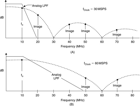
Assume that we increase the DAC update rate to 60 MSPS and insert a “zero” between each original data sample. The parallel data stream is now 60 MSPS, but we must now determine the value of the zero-value data points. This is done by passing the 60 MSPS data stream with the added zeros through a digital interpolation filter which computes the additional data points. The response of the digital filter relative to the 2-times oversampling frequency is shown in Figure 6-35(B). The analog antialiasing filter transition zone is now 10–50 MHz (the first image occurs at 2fc − fo = 60−10 = 50 MHz). This transition zone is a little greater than 2 octaves, implying that a 5- or 6-pole Butterworth filter is sufficient.
The AD9773/AD9775/AD9777 (12/14/16-bit) series of Transmit DACs (TxDAC™) are selectable 2 times, 4 times, or 8 times oversampling interpolating dual DACs, and a simplified block diagram is shown in Figure 6-36. These devices are designed to handle 12/14/16-bit input word rates up to 160 MSPS. The output word rate is 400 MSPS maximum. For an output frequency of 50 MHz, an input update rate of 160 MHz, and an oversampling ratio of 2 times, the image frequency occurs at 320 MHz −50 MHz = 270 MHz. The transition band for the analog filter is therefore 50–270 MHz. Without 2 times oversampling, the image frequency occurs at 160 MHz −50 MHz = 110 MHz, and the filter transition band is 60–110 MHz.

Reconstruction Filters
The output of a DAC is not a continuously varying waveform, but instead a series of DC levels. This output must be passed through a filter to remove the high frequency components and smooth waveform into a more truly analog waveform.
The concept of filtering is discussed in more detail in Chapter 8.
In general, to preserve spectral purity, the images of the DAC output must be attenuated below the resolution of DAC. To use the example sited above, we assume that the DAC output passband is 10 MHz. The sample rate is 30 MHz. Therefore the image of the passband that must be attenuated is 30 MHz −10 MHz = 20 MHz. This is the sample rate minus the passband frequency. The DAC in this example is a 10-bit device, which would indicate a distortion level of −60 dB. So a reconstruction filter should reduce the image by 60 dB while not attenuating the fundamental at all. Since a filter attenuates at 6 dB/pole, this would indicate that a tenth-order filter would be required.
There are several other considerations that must be taken into account.
First is that most filter cutoffs are measured at the −3 dB point. Therefore, if we do not want the fundamental attenuated, some margin in the filter is required. The graphs in the filter section will help illustrate this point. This will cause the transition band to become narrower and thus the order of the filter to increase.
Sin(x)/(x)(Sinc)
The output of a DAC is not a continually varying waveform but instead a series of DC levels. The DAC puts out a DC level until it is told to put out a new level. This is illustrated in Figure 6-37.

The width of the pulses is 1/FS. The spectrum of each pulse is the sin(x)/x curve. This is also known as the sinc curve. This response is added to the response of the reconstruction filter to provide the overall response of the converter. This will cause an amplitude error as the output frequency approaches the Nyquist frequency (FS/2). The value of the sinc function is shown in Figure 6-38. Some high speed DACs incorporate an inverse filter (in the digital domain) to compensate for this rolloff.

Intentionally Nonlinear DACs
Thus far, we have emphasized the importance of maintaining good differential and integral linearity. However, there are situations where ADCs and DACs which have been made intentionally nonlinear (but maintaining good differential linearity) are useful, especially when processing signals having a wide dynamic range. One of the earliest uses of nonlinear data converters was in the digitization of voiceband signals for pulse code modulation (PCM) systems. Major contributions were made at Bell Labs during the development of the T1 carrier system. The motive for the nonlinear ADCs and DACs was to reduce the total number of bits (and therefore the serial transmission rate) required to digitize voice channels. Straight linear encoding of a voice channel required 11 or 12 bits at an 8 kSPS per channel sampling rate. In the 1960s Bell Labs determined that 7-bit nonlinear encoding was sufficient, and later in the 1970s went to 8-bit nonlinear encoding for better performance.
The nonlinear transfer function allocates more quantization levels out of the total range for small signals and fewer for large amplitude signals. In effect, this reduces the quantization noise associated with small signals (where it is most noticeable) and increases the quantization noise for larger signals (where it is less noticeable). The term companding is generally used to describe this form of encoding.
The logarithmic transfer function chosen is referred to as the “Bell μ-255” standard, or simply “μ-law.” A similar standard developed in Europe is referred to as “A-law.” The Bell μ-law allows a dynamic range of about 4,000:1 using 8 bits, whereas an 8-bit linear data converter provides a range of only 256:1.
The first generation channel bank (D1) used temperature-controlled resistor-diode networks for “compressors” ahead of a 7-bit linear ADC in the transmitter to generate the logarithmic transfer function. Corresponding resistor-diode “expandors” having an inverse transfer function followed the 7-bit linear DAC in the receiver. The next generation D2 channel banks used nonlinear ADCs and DACs to accomplish the compression/expansion functions in a much more reliable and cost-effective manner and eliminated the need for the temperature-controlled diode networks.
In his 1953 classic paper, B.D. Smith proposed that the transfer function of a successive approximation ADC utilizing a nonlinear internal DAC in the feedback path would be the inverse transfer function of the DAC (Reference 8). The same basic DAC could therefore be used in the ADC and also for the reconstruction DAC. Later in the 1960s and early 1970s, nonlinear ADC and DAC technology using piecewise linear approximations of the desired transfer function allowed low cost high volume implementations (References 18–23). These nonlinear 8-bit, 8-kSPS data converters became popular telecommunications building blocks.
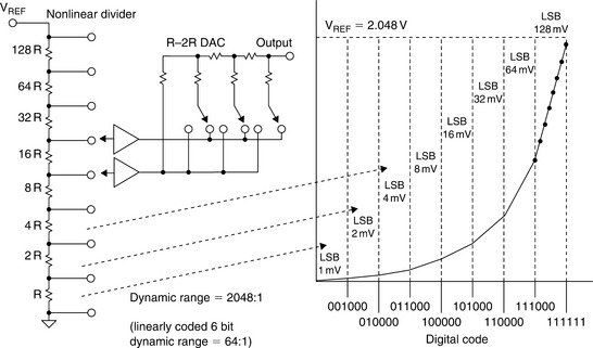
The nonlinear transfer function of the 8-bit DAC is first divided into 16 segments (chords) of different slopes—the slopes are determined by the desired nonlinear transfer function. The 4 MSBs determine the segment containing the desired data point, and the individual segment is further subdivided into 16 equal quantization levels by the 4 LSBs of the 8-bit word. This is shown in Figure 6-39 for a 6-bit DAC, where the first 3 bits identify one of the 8 possible chords, and each chord is further subdivided into 8 equal levels defined by the 3 LSBs. The 3 MSBs are generated using a nonlinear string DAC, and the 3 LSBs are generated using a 3-bit binary R–2R DAC.
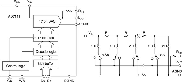
In 1982, Analog Devices introduced the LOGDAC™ AD7111 monolithic MDAC featuring wide dynamic range using a logarithmic transfer function. The basic DAC in the LOGDAC is a linear 17-bit voltage-mode R–2R DAC preceded by an 8-bit input decoder (a functional diagram of the LOGDAC is shown in Figure 6-40). The LOGDAC can attenuate an analog input signal, VIN, over the range 0–88.5 dB in 0.375 dB steps. The degree of attenuation across the DAC is determined by a nonlinear-coded 8-bit word applied to the onboard decode logic. This 8-bit word is mapped into the appropriate 17-bit word which is then applied to a 17-bit, R–2R ladder. In addition to providing the logarithmic transfer function, the LOGDAC also acts as a full four-quadrant MDAC.
With the introduction of high resolution linear ADCs and DACs, the method used in the LOGDAC™ is widely used today to implement various nonlinear transfer functions such as the μ-law and A-law companding functions required for telecommunications and other applications. Figure 6-41 shows a general block diagram of the modern approach. The μ-law or A-law companded input data is mapped into data points on the transfer function of a high resolution DAC. This mapping can be easily accomplished by a simple lookup table in either hardware, software, or firmware. A similar nonlinear ADC can be constructed by digitizing the analog input signal using a high resolution ADC and mapping the data points into a shorter word using the appropriate transfer function. A big advantage of this method is that the transfer curve does not have to be approximated with straight line segments as in the earlier method, thereby providing more accuracy.

SECTION 6-2 ADC Architectures
The basic ADC function is shown in Figure 6-42. This could also be referred to as a quantizer. Most ADC chips also include some of the support circuitry, such as clock oscillator for the sampling clock, reference (REF), the SHA function, and output data latches. In addition to these basic functions, some ADCs have additional circuitry built in. These functions could include multiplexers, sequencers, auto-calibration circuits, programmable gain amplifiers (PGAs), etc.
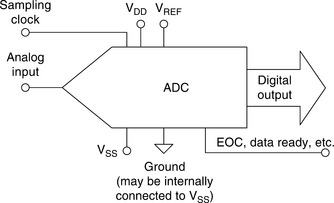
Similar to DACs, some ADCs use external references and have a reference input terminal, while others have an output from an internal reference. In some instances the ADC may have an internal reference that is pinned out through a resistor. This connection allows the reference to be filtered (using the internal R and an external C) or by allowing the internal reference to be overdriven by an external reference. The AD789X family of parts are examples of ADC that use this type of connection. The simplest ADCs, of course, have neither—the reference is on the ADC chip and has no external connections.
If an ADC has an internal reference, its overall accuracy is specified when using that reference. If such an ADC is used with a perfectly accurate external reference, its absolute accuracy may actually be worse than when it is operated with its own internal reference. This is because it is trimmed for absolute accuracy when working with its own actual reference voltage, not with the nominal value. Twenty years ago it was common for converter references to have accuracies as poor as ±5% since these references were trimmed for low temperature coefficient rather than absolute accuracy, and the inaccuracy of the reference was compensated in the gain trim of the ADC itself. Today the problem is much less severe, but it is still important to check for possible loss of absolute accuracy when using an external reference with an ADC which has a built-in one.
ADCs which have reference terminals must, of course, specify their behavior and parameters. If there is a reference input the first specification will be the reference input voltage—and of course this has two values, the absolute maximum rating, and the range of voltages over which the ADC performs correctly.
Most ADCs require that their reference voltage is within quite a narrow range whose maximum value is less than or equal to the ADC’s VDD.
The reference input terminal of an ADC may be buffered as shown in Figure 6-43, in which case it has input impedance (usually high) and bias current (usually low) specifications, or it may connect directly to the ADC. In either case, the transient currents developed on the reference input due to the internal conversion process need good decoupling with external low inductance capacitors. Good ADC data sheets recommend appropriate decoupling networks.

The reference output may be buffered or unbuffered. If it is buffered, the maximum output current will probably be specified. In general such a buffer will have a unidirectional output stage which sources current but does not allow current to flow into the output terminal. If the buffer does have a push–pull output stage (not as common), the output current will probably be defined as ± (some value) mA. If the reference output is unbuffered, the output impedance may be specified, or the data sheet may simply advise the use of a high input impedance external buffer.
There are some instances where the power supply is the reference. In these cases it is imperative to make sure the power supply is clean.
The sampling clock input is a critical function in an ADC and a source of some confusion. It could truly be the sampling clock. This frequency would typically be several times higher than the sampling rate of the converter. It could also be a convert start (or encode) command which would happen once per conversion. Pipeline architecture devices and sigma–delta (ΣΔ) converters are continuously converting and have no convert start command.
Regardless of the ADC, it is extremely important to read the data sheet and determine exactly what the external clock requirements are, because they can vary widely from one ADC to another.
At some point after the assertion of the sampling clock, the output data is valid. This data may be in parallel or serial format depending on the ADC. Early successive approximation ADCs such as the AD574 simply provided a STATUS output (STS) which went high during the conversion, and returned to the low state when the output data was valid. In other ADCs, this line is variously called busy, end-of-conversion (EOC), data ready (DRDY), etc. Regardless of the ADC, there must be some method of knowing when the output data is valid—and again, the data sheet is where this information can always be found.
Another detail which can cause trouble is the difference between EOC and DRDY. EOC indicates that conversion has finished, DRDY that data is available at the output. In some ADCs, EOC functions as DRDY—in others, data is not valid until several tenths of nanoseconds after the EOC has become valid, and if EOC is used as a data strobe, the results will be unreliable.
There are one or two other practical points which are worth remembering about the logic of ADCs. On power-up, many ADCs do not have logic reset circuitry and may enter an anomalous logical state. Several conversions may be necessary to restore their logic to proper operation so: (a) the first few conversions after power-up should never be trusted, and (b) control outputs (EOC, DRDY, etc.) may behave in unexpected ways at this time (and not necessarily in the same way at each power-up), and (c) care should be taken to ensure that such anomalous behavior cannot cause system latch-up. For example, EOC should not be used to initiate conversion if there is any possibility that EOC will not occur until the first conversion has taken place, as otherwise initiation will never occur.
Some low power ADCs now have power-saving modes of operation variously called standby, power-down, sleep, etc. When an ADC comes out of one of these low power modes, there is a certain recovery time required before the ADC can operate at its full specified performance. The data sheet should therefore be carefully studied when using these modes of operation.
As a final example, some ADCs use CS (chip select) edges to reset internal logic, and it may not be possible to perform another conversion without asserting or reasserting CS (or it may not be possible to read the same data twice, or both).
For more detail, it is important to read the whole data sheet before using an ADC since there are innumerable small logic variations from type to type. Unfortunately, many data sheets are not as clear as one might wish, so it is also important to understand the general principles of ADCs in order to interpret data sheets correctly. That is one of the purposes of this section.
There are a couple of general trend in ADCs that should be addressed. The first is the general trend toward lower supply voltages. This is partially due to the processes, particularly CMOS, which are used to manufacture the chips. Increasing demand for speed has driven the feature size of the processes down. This typically results in lower breakdown voltages for the transistors. This, in turn, requires lower supply voltages. Very few new parts are developed with the legacy ± 15 V supplies and ± 10 V input range.
Since the input signal range of the ADCs is shrinking, there is also a trend toward differential inputs. This helps improve the dynamic range of a converter, typically by 6 dB. There could be even further improvement since the common-mode ground-referenced noise is rejected. In many cases the differential input can be driven single endedly (with the resultant reduction of SNR). Occasionally the REF input might also be differential.
The Comparator: A 1-Bit ADC
A comparator is a 1-bit ADC (see Figure 6-44). If the input is above a threshold, the output has one logic value, below it has another. There is no ADC architecture which does not use at least one comparator of some sort. So while a 1-bit ADC is of very limited usefulness it is a building block for other architectures.

Comparators used as building blocks in ADCs need good resolution which implies high gain. This can lead to uncontrolled oscillation when the differential input approaches zero. In order to prevent this, hysteresis is often added to comparators using a small amount of positive feedback. Figure 6-44 shows the effects of hysteresis on the overall transfer function. Many comparators have a millivolt or two of hysteresis to encourage “snap” action and to prevent local feedback from causing instability in the transition region. Note that the resolution of the comparator can be no less than the hysteresis, so large values of hysteresis are generally not useful.
Successive Approximation ADCs
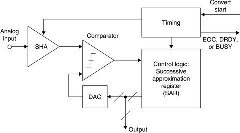
The successive approximation ADC has been the mainstay of data acquisition for many years. Recent design improvements have extended the sampling frequency of these ADCs into the megahertz region.
The basic successive approximation ADC is shown in Figure 6-45. It performs conversions on command. On the assertion of the CONVERT START command, the SHA is placed in the hold mode, and all the bits of the successive approximation register (SAR) are reset to “0” except the MSB which is set to “1.” The SAR output drives the internal DAC. If the DAC output is greater than the analog input, this bit in the SAR is reset, otherwise it is left set. The next MSB is then set to “1.” If the DAC output is greater than the analog input, this bit in the SAR is reset, otherwise it is left set. The process is repeated with each bit in turn. When all the bits have been set, tested, and reset or not as appropriate, the contents of the SAR correspond to the value of the analog input, and the conversion is complete. These bit “tests” can form the basis of a serial output version SAR-based ADC.
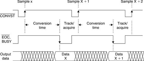
The fundamental timing diagram for a typical SAR ADC is shown in Figure 6-46. The EOC is generally indicated by an EOC, DRDY, or a busy signal (actually, not-BUSY indicates EOC). The polarities and name of this signal may be different for different SAR ADCs, but the fundamental concept is the same. At the beginning of the conversion interval, the signal goes high (or low) and remains in that state until the conversion is completed, at which time it goes low (or high). The trailing edge is generally an indication of valid output data, but the data sheet should be carefully studied—in some ADCs additional delay is required before the output data is valid.
An N-bit conversion takes N steps. It would seem on superficial examination that a 16-bit converter would have twice the conversion time of an 8-bit one, but this is not the case. In an 8-bit converter, the DAC must settle to 8-bit accuracy before the bit decision is made, whereas in a 16-bit converter, it must settle to 16-bit accuracy, which takes a lot longer. In practice, 8-bit successive approximation ADCs can convert in a few hundred nanoseconds, while 16-bit ones will generally take several microseconds.
While there are some variations, the fundamental timing of most SAR ADCs is similar and relatively straightforward. The conversion process is initiated by asserting a CONVERT START signal. This signal is typically named something like ![]() or CS. This signal is usually a negative-going pulse whose positive-going edge actually initiates the conversion. The internal SHA is placed in the hold mode on this edge, and the various bits are determined using the SAR algorithm. The negative-going edge of the
or CS. This signal is usually a negative-going pulse whose positive-going edge actually initiates the conversion. The internal SHA is placed in the hold mode on this edge, and the various bits are determined using the SAR algorithm. The negative-going edge of the ![]() pulse causes a signal typically called
pulse causes a signal typically called ![]() or BUSY to go high. When the conversion is complete, the BUSY line goes low (or
or BUSY to go high. When the conversion is complete, the BUSY line goes low (or ![]() goes high), indicating the completion of the conversion process. In most cases the trailing edge of the BUSY line can be used as an indication that the output data is valid and can be used to strobe the output data into an external register.
goes high), indicating the completion of the conversion process. In most cases the trailing edge of the BUSY line can be used as an indication that the output data is valid and can be used to strobe the output data into an external register.
There may also be other control lines. And sometimes control lines have dual function. This is primarily done when the chip is pin limited. Because of the many variations in terminology and design, the individual data sheet should always be consulted when using a specific ADC.
It should also be noted that some SAR ADCs require an external high frequency clock in addition to the CONVERT START command. In most cases, there is no need to synchronize the two. The frequency of the external clock, if required, generally falls in the range of 1–30 MHz depending on the conversion time and resolution of the ADC. Other SAR ADCs have an internal oscillator which is used to perform the conversions and only requires the CONVERT START command. Because of their architecture, SAR ADCs generally allow single-shot conversion at any repetition rate from DC to the converter’s maximum conversion rate.
Notice that the overall accuracy and linearity of the SAR ADC is determined primarily by the internal DAC. Until recently, most precision SAR ADCs used laser-trimmed thin-film DACs to achieve the desired accuracy and linearity. The thin-film resistor trimming process adds cost, and the thin-film resistor values may be affected when subjected to the mechanical stresses of packaging.
For these reasons, switched capacitor (or charge redistribution) DACs have become popular in newer SAR ADCs. The advantage of the switched capacitor DAC is that the accuracy and linearity are primarily determined by photolithography, which in turn controls the capacitor plate area and the capacitance as well as matching. In addition, small capacitors can be placed in parallel with the main capacitors which can be switched in and out under control of autocalibration routines to achieve high accuracy and linearity without the need for thin-film laser trimming. Temperature tracking between the switched capacitors can be better than 1 ppm/°C, thereby offering a high degree of temperature stability.
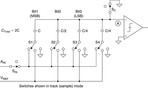
A simple 3-bit capacitor DAC is shown in Figure 6-47. The switches are shown in the track, or sample mode where the analog input voltage, AIN, is constantly charging and discharging the parallel combination of all the capacitors. The hold mode is initiated by opening SIN, leaving the sampled analog input voltage on the capacitor array. Switch SC is then opened allowing the voltage at node A to move as the bit switches are manipulated. If S1, S2, S3, and S4 are all connected to ground, a voltage equal to –AIN appears at node A. Connecting S1 to VREF adds a voltage equal to VREF/2 to –AIN. The comparator then makes the MSB bit decision, and the SAR either leaves S1 connected to VREF or connects it to ground depending on the comparator output (which is high or low depending on whether the voltage at node A is negative or positive, respectively). A similar process is followed for the remaining two bits. At the EOC interval, S1, S2, S3, S4, and SIN are connected to AIN, SC is connected to ground, and the converter is ready for another cycle.

Note that the extra LSB capacitor (C/4 in the case of the 3-bit DAC) is required to make the total value of the capacitor array equal to 2C so that binary division is accomplished when the individual bit capacitors are manipulated.
The operation of the capacitor DAC (cap DAC) is similar to an R–2R resistive DAC. When a particular bit capacitor is switched to VREF, the voltage divider created by the bit capacitor and the total array capacitance (2C) adds a voltage to node A equal to the weight of that bit. When the bit capacitor is switched to ground, the same voltage is subtracted from node A.
An example of charge redistribution successive approximation ADCs is Analog Devices’ PulSAR™ series. The AD7677 is a 16-bit, 1 MSPS, PulSAR, fully differential ADC that operates from a single 5 V power supply (see Figure 6-48). The part contains a high speed 16-bit sampling ADC, an internal conversion clock, error correction circuits, and both serial and parallel system interface ports. The AD7677 is hardware factory calibrated and comprehensively tested to ensure such AC parameters as SNR and total harmonic distortion (THD), in addition to the more traditional DC parameters of gain, offset, and linearity. It features a very high sampling rate mode (Warp) and, for asynchronous conversion rate applications, a fast mode (Normal) and, for low power applications, a reduced power mode (Impulse) where the power is scaled with the throughput.

The operation of a successive approximation ADC is as follows. Using Figure 6-49 as an example, one side of the balance is loaded with half-scale (in this case 32 lbs.). Call this the proof mass. The test mass is then put on the other side of the balance. If the test mass is greater, as it is in this case, the proof mass is retained, otherwise it is discarded. Next a proof mass equal to 1/4 scale is added. Again, if the test mass is still greater the proof mass is retained, otherwise it is rejected. In the example it is rejected. This process is continued, each time cutting the proof mass in half, until the desired resolution is reached. The proof masses are added up. This will equal the mass of the test mass, to the resolution of the test.
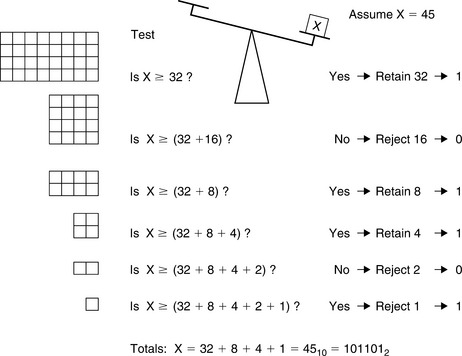
In an SAR ADC the proof mass is a voltage provided by the DAC. It is compared to the input, corresponding to the test mass, by the comparator. Keeping track of output of each test and setting the DAC is accomplished by the SAR.
The digital output is basically serial in nature, but SAR ADCs are generally available in both serial and parallel output formats.
Flash Converters
Flash ADCs (sometimes called parallel ADCs) are the fastest type of ADC and use large numbers of comparators. An N-bit flash ADC consists of 2N resistors and 2N–1 comparators arranged as in Figure 6-50. Each comparator has a reference voltage which is 1 LSB higher than that of the one below it in the chain. For a given input voltage, all the comparators below a certain point will have their input voltage larger than their reference voltage and a “1” logic output, and all the comparators above that point will have a reference voltage larger than the input voltage and a “0” logic output. The 2N–1 comparator outputs therefore behave in a way analogous to a mercury thermometer, and the output code at this point is sometimes called a thermometer code. Since 2N–1 data outputs are not really practical, they are processed by a decoder to generate an N-bit binary output.
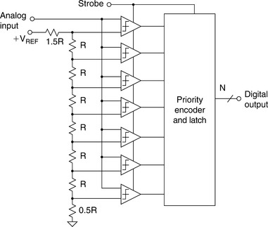
The input signal is applied to all the comparators at once, so the thermometer output is delayed by only one comparator delay from the input, and the encoder N-bit output by only a few gate delays on top of that, so the process is very fast. However, the architecture uses large numbers of resistors and comparators and is limited to low resolutions, and if it is to be fast, each comparator must run at relatively high power levels. Hence, the problems of flash ADCs include limited resolution, high power dissipation because of the large number of high speed comparators (especially at sampling rates greater than 50 MSPS), and relatively large (and therefore expensive) chip sizes. In addition, the resistance of the reference resistor chain must be kept low to supply adequate bias current to the fast comparators, so the voltage reference has to source quite large currents (typically >10 mA).
Each comparator has a voltage-variable junction capacitance, and this signal-dependent capacitance results in most flash ADCs having reduced effective number of bits (ENOB) and higher distortion at high input frequencies. For this reason, most flash converters must be driven with a wideband op amp which is tolerant to the capacitive load presented by the converter as well as high speed transients developed on the input.
Power dissipation is always a big consideration in flash converters, especially at resolutions above 8 bits. A clever technique was used for AD9410 10-bit, 210 MSPS ADC called interpolation to minimize the number of preamplifiers in the flash converter comparators and also reduce the power (2.1 W). The method is shown in Figure 6-51 (see reference).
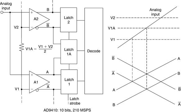
The preamplifiers (labeled “A1,” “A2,” etc.) are low gain gm stages whose bandwidth is proportional to the tail currents of the differential pairs. Consider the case for a positive-going ramp input which is initially below the reference to AMPA1, V1. As the input signal approaches V1, the differential output of A1 approaches zero (i.e., A = Ā), and the decision point is reached. The output of A1 drives the differential input of LATCH 1. As the input signal continues to go positive, A continues to go positive, and ![]() begins to go negative. The interpolated decision point is determined when A =
begins to go negative. The interpolated decision point is determined when A = ![]() . As the input continues positive, the third decision point is reached when B =
. As the input continues positive, the third decision point is reached when B = ![]() . This novel architecture reduces the ADC input capacitance and thereby minimizes its change with signal level and the associated distortion. The AD9410 also uses an input SHA circuit for improved AC linearity.
. This novel architecture reduces the ADC input capacitance and thereby minimizes its change with signal level and the associated distortion. The AD9410 also uses an input SHA circuit for improved AC linearity.
Subranging, Error Corrected, and Pipelined ADCs
A basic two-stage N bit subranging ADC is shown in Figure 6-52. The ADC is based on two separate conversions—a coarse conversion (N1 bits) in the MSB sub-ADC (SADC) followed by a fine conversion (N2 bits) in the LSB SADC. Early subranging ADCs nearly always used flash converters as building blocks, but a number of recent ADCs utilize other architectures for the individual ADCs.
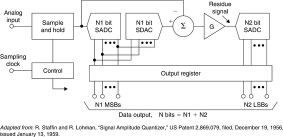
The conversion process begins placing the SHA in the hold mode followed by a coarse N1-bit SADC conversion of the MSBs. The digital outputs of the MSB converter drive an N1-bit sub-DAC (SDAC) which generates a coarsely quantized version of the analog input signal. The N1-bit SDAC output is subtracted from the held analog signal, amplified, and applied to the N2-bit LSB SADC. The amplifier provides gain, G, sufficient to make the “residue” signal exactly fill the input range of the N2 SADC. The output data from the N1 SADC and the N2 SADC are latched into the output registers yielding the N-bit digital output code, where N = N1 + N2.
In order for this simple subranging architecture to work satisfactorily, both the N1 SADC and SDAC (although they only have N1 bits of resolution) must be better than N bits accurate. The residue signal offset and gain must be adjusted such that it precisely fills the range of the N2 SADC as shown in Figure 3-66(A). If the residue signal drifts by more than 1 LSB (referenced to the N2 SADC), then there will be missing codes as shown in Figure 6-53(A) where the residue signal enters the out-of-range regions labeled “X” and “Y.” Any nonlinearity or drift in the N1 SADC will also cause missing codes if it exceeds 1 LSB referenced to N bits. In practice, an 8 bit subranging ADC with N1 = 4 bits and N2 = 4 bits represents a realistic limit to this architecture in order to maintain no missing codes over a reasonable operating temperature range.


When the interstage alignment is not correct, missing codes will appear in the overall ADC transfer function as shown in Figure 6-54. If the residue signal goes into positive overrange (the “X” region), the output first “sticks” on a code and then “jumps” over a region leaving missing codes. The reverse occurs if the residue signal is negative overrange.

In order to reliably achieve higher than 8-bit resolution using the subranging approach, a technique generally referred to as digital corrected subranging, digital error correction, overlap bits, redundant bits, etc. is utilized.
Figure 6-55 shows two methods that can be used to design a pipeline stage in a subranging ADC. Figure 6-55 shows two pipelined stages which use an interstage T/H in order to provide interstage gain and give each stage the maximum possible amount of time to process the signal at its input. In Figure 6-55(B) an MDAC is used to provide the appropriate amount of interstage gain as well as the subtraction function.

The term “pipelined” architecture refers to the ability of one stage to process data from the previous stage during any given clock cycle. At the end of each phase of a particular clock cycle, the output of a given stage is passed on to the next stage using the T/H functions and new data is shifted into the stage. Of course this means that the digital outputs of all but the last stage in the “pipeline” must be stored in the appropriate number of shift registers so that the digital data arriving at the correction logic corresponds to the same sample.
Figure 6-56 shows a timing diagram of a typical pipelined subranging ADC. Notice that the phases of the clocks to the T/H amplifiers are alternated from stage to stage such that when a particular T/H in the ADC enters the hold mode it holds the sample from the preceding T/H, and the preceding T/H returns to the track mode. The held analog signal is passed along from stage to stage until it reaches the final stage in the pipelined ADC—in this case, a flash converter. When operating at high sampling rates, it is critical that the differential sampling clock be kept at a 50% duty cycle for optimum performance. Duty cycles other than 50% affect all the T/H amplifiers in the chain—some will have longer than optimum track times and shorter than optimum hold times; while others suffer exactly the reverse condition. Several newer pipelined ADCs including the 12-bit, 65 MSPS AD9235 and the 12-bit, 210 MSPS AD9430 have on-chip clock conditioning circuits to control the internal duty cycle while allowing some variation in the external clock duty cycle.

The effects of the “pipeline” delay (sometimes called latency) in the output data are shown in Figure 6-57 for the AD9235 12-bit 65 MSPS ADC where there is a seven-clock cycle pipeline delay.
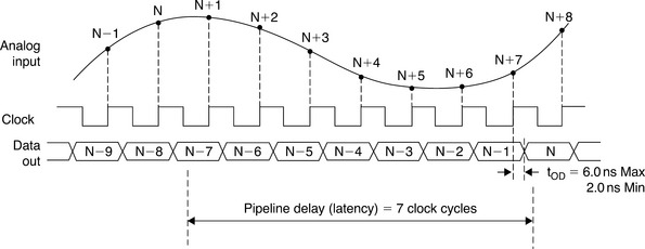
Note that the pipeline delay is a function of the number of stages and the particular architecture of the ADC under consideration—the data sheet should always be consulted for the exact details of the relationship between the sampling clock and the output data timing. In many applications the pipeline delay will not be a problem, but if the ADC is inside a feedback loop the pipeline delay may cause instability. The pipeline delay can also be troublesome in multiplexed applications or when operating the ADC in a “single-shot” mode. Other ADC architectures—such as successive approximation—may be better suited to these types of applications.
The pipelined error correcting ADC has become very popular in modern ADCs requiring wide dynamic range and low levels of distortion. There are many possible ways to design a pipelined ADC, and we will now look at just a few of the tradeoffs. Figure 6-58(A) shows a pipelined ADC designed with identical stages of k-bits each. This architecture uses the same core hardware in each stage, offers a few other advantages, but does necessarily optimize the ADC for best possible performance. Figure 6-58(B) shows the simplest form of this architecture where k = 1.
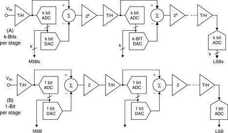
In order to optimize performance at the 12-bit level, e.g., 1-bit-per-stage pipeline is more commonly used with a multibit front-end and back-end ADC as shown in Figure 6-59.
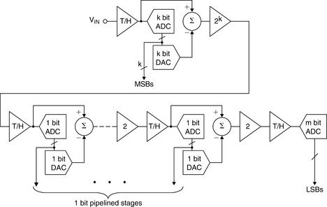
Another less popular type of error corrected subranging architecture is the recirculating subranging ADC (Figure 6-60). The concept is similar to the error corrected subranging architecture previously discussed, but in this architecture, the residue signal is recirculated through a single ADC and DAC stage using switches and a PGA. The major problem with this technique is the PGA. Its gain-bandwidth product will limit the frequency response at higher gains. Also matching of the various gains could be problematic.

Serial Bit-per-Stage Binary and Gray Coded (Folding) ADCs
Various architectures exist for performing A/D conversion using one stage per bit. Figure 6-61 shows the overall concept. In fact, a multistage subranging ADC with 1 bit-per-stage and no error correction is one form as previously discussed. In this approach, the input signal must be held constant during the entire conversion cycle. There are N stages, each of which have a bit output and a residue output. The residue output of one stage is the input to the next. The last bit is detected with a single comparator as shown.

Figure 6-61: Generalized bit-per-stage ADC architecture
Adapted from: B. D. Smith, “An Unusual Electronic Analog–Digital Conversion Method” IRE Transactions on Instrumentation, June 1956, pp. 155–160.
The basic stage for performing a single binary bit conversion is shown in Figure 6-62. It consists of a gain-of-two amplifier, a comparator, and a 1-bit DAC. Assume that this is the first stage of the ADC. The MSB is simply the polarity of the input, and that is detected with the comparator which also controls the 1-bit DAC. The 1-bit DAC output is summed with the output of the gain-of-two amplifier. The resulting residue output is then applied to the next stage. In order to better understand how the circuit works, the diagram shows the residue output for the case of a linear ramp input voltage which traverses the entire ADC range, − VR to + VR. Notice that the polarity of the residue output determines the binary bit output of the next stage.
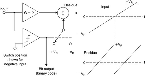
A simplified 3-bit serial-binary ADC is shown in Figure 6-63, and the residue outputs are shown in Figure 6-64. Again, the case is shown for a linear ramp input voltage whose range is between − VR and + VR. Each residue output signal has discontinuities which correspond to the point where the comparator changes state and causes the DAC to switch. The fundamental problem with this architecture is the discontinuity in the residue output waveforms. Adequate settling time must be allowed for these transients to propagate through all the stages and settle at the final comparator input. As presented here, the prospects of making this architecture operate at high speed are dismal. However using the 1.5 bit-per-stage pipelined architecture previously discussed in this section makes it much more attractive at high speeds.


Although the binary method is discussed in his paper, B. D. Smith also describes a much preferred bit-per-stage architecture based on absolute value amplifiers (magnitude amplifiers, or simply MagAMPs™). This scheme has often been referred to as serial-Gray (since the output coding is in Gray code), or folding converter because of the shape of the transfer function. Performing the conversion using a transfer function that produces an initial Gray code output has the advantage of minimizing discontinuities in the residue output waveforms and offers the potential of operating at much higher speeds than the binary approach.
The basic folding stage is shown functionally in Figure 6-65 along with its transfer function. The input to the stage is assumed to be a linear ramp voltage whose range is between −VR and + VR. The comparator detects the polarity of the input signal and provides the Gray bit output for the stage. It also determines whether the overall stage gain is + 2 or −2. The reference voltage VR is summed with the switch output to generate the residue signal which is applied to the next stage. The polarity of the residue signal determines the Gray bit for the next stage. The transfer function for the folding stage is also shown in Figure 6-65.
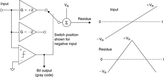
A 3-bit MagAMP folding ADC is shown in Figure 6-66, and the corresponding residue waveforms in Figure 6-67. As in the case of the binary ripple ADC, the polarity of the residue output signal of a stage determines the value of the Gray bit for the next stage. The polarity of the input to the first stage determines the Gray MSB; the polarity of R1 output determines the Gray bit-2; and the polarity of R2 output determines the Gray bit-3. Notice that unlike the binary ripple ADC, there is no abrupt transition in any of the folding stage residue output waveforms. This makes operation at high speeds quite feasible.

Modern IC circuit designs implement the transfer function using current-steering open-loop gain techniques which can be made to operate much faster. Fully differential stages (including the SHA) also provide speed, lower distortion, and yield 8 bit accurate folding stages with no requirement for thin-film resistor laser trimming.
An example of a fully differential gain-of-two MagAMP folding stage is shown in Figure 6-68. The differential input signal is applied to the degenerated-emitter differential pair Q1, Q2 and the comparator. The differential input voltage is converted into a differential current which flows in the collectors of Q1, Q2. If + IN is greater than −IN, cascode-connected transistors Q3, Q6 are on, and Q4, Q6 are off. The differential signal currents therefore flow through the collectors of Q3, Q6 into level-shifting transistors Q7, Q8 and into the output load resistors, developing the differential output voltage between +OUT and –OUT. The overall differential voltage gain of the circuit is two.

If + IN is less than −IN (negative differential input voltage), the comparator changes stage and turns Q4, Q5 on and Q3, Q6 off. The differential signal currents flow from Q5 to Q7 and from Q4 to Q8, thereby maintaining the same relative polarity at the differential output as for a positive differential input voltage. The required offset voltage is developed by adding a current IOFF to the emitter current of Q7 and subtracting it from the emitter current of Q8.
The differential residue output voltage of the stage drives the next stage input, and the comparator output represents the Gray code output for the stage.
The MagAMP architecture offers lower power and can be extended to sampling rates previously dominated by flash converters. For example, the AD9054A 8-bit, 200 MSPS ADC is shown in Figure 6-69. The first 5 bits (Gray code) are derived from five differential MagAMP stages. The differential residue output of the fifth MagAMP stage drives a 3-bit flash converter, rather than a single comparator.

The Gray-code output of the five MagAMPs and the binary-code output of the 3-bit flash are latched, all converted into binary, and latched again in the output data register. Because of the high data rate, a demultiplexed output option is provided.
Counting and Integrating ADC Architectures
Although counting-based ADCs are not well suited for high speed applications, they are ideal for high resolution low frequency applications, especially when combined with integrating techniques.
The counting ADC technique (see Figure 6-70) basically uses a sampling pulse to take a sample of the analog signal, set an R/S flip-flop, and simultaneously start a controlled ramp voltage. The ramp voltage is compared with the input, and when they are equal, a pulse is generated which resets the R/S flip-flop. The output of the flip-flop is a pulse whose width is proportional to the analog signal at the sampling instant. This pulse width modulated (PWM) pulse controls a gated oscillator, and the number of pulses out of the gated oscillator represents the quantized value of the analog signal. This pulse train can be easily converted to a binary word by driving a counter. In Reeves’ system, a master clock of 600 kHz was used, and a 100:1 divider generated the 6 kHz sampling pulses. The system uses a 5-bit counter, and 31 counts (out of the 100 counts between sampling pulses) therefore represent a full-scale signal. The technique can obviously be extended to higher resolutions.
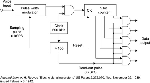
Charge Run-Down ADCs
The charge run-down ADC architecture shown in Figure 6-71 first samples the analog input and stores the voltage on a fixed capacitor. The capacitor is then discharged with a constant current source, and the time required for complete discharge is measured using a counter. Notice that in this approach, the overall accuracy is dependent on the magnitude of the capacitor, the magnitude of the current source, as well as the accuracy of the timebase.
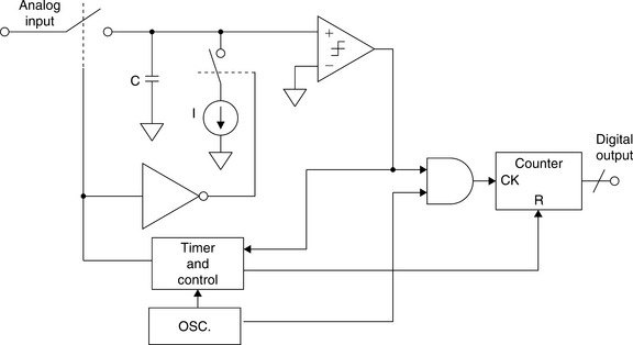
Ramp Run-Up ADCs
In the ramp run-up architecture shown in Figure 6-72, a ramp generator is started at the beginning of the conversion cycle. The counter then measures the time required for the ramp voltage to equal the analog input voltage. The counter output is therefore proportional to the value of the analog input. In an alternate version (shown dotted in Figure 6-72), the ramp voltage generator is replaced by a DAC which is driven by the counter output. The advantage of using the ramp is that the ADC is always monotonic, whereas overall monotonicity is determined by the DAC when it is used as a substitute.

The accuracy of the ramp run-up ADC depends on the accuracy of the ramp generator (or the DAC) as well as the oscillator.
Tracking ADCs
The tracking ADC architecture shown in Figure 6-73 continually compares the input signal with a reconstructed representation of the input signal. The up/down counter is controlled by the comparator output. If the analog input exceeds the DAC output, the counter counts up until they are equal. If the DAC output exceeds the analog input, the counter counts down until they are equal. It is evident that if the analog input changes slowly, the counter will follow, and the digital output will remain close to its correct value. If the analog input suddenly undergoes a large step change, it will be many hundreds or thousands of clock cycles before the output is again valid. The tracking ADC therefore responds quickly to slowly changing signals, but slowly to a quickly changing one.
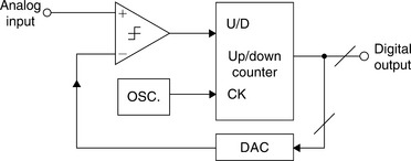
The simple analysis above ignores the behavior of the ADC when the analog input and DAC output are nearly equal. This will depend on the exact nature of the comparator and counter. If the comparator is a simple one, the DAC output will cycle by 1 LSB from just above the analog input to just below it, and the digital output will, of course, do the same—there will be 1 LSB of flicker. Note that the output in such a case steps every clock cycle, irrespective of the exact value of analog input, and hence always has unity mark-space ratio. In other words, there is no possibility of taking a mean value of the digital output and increasing resolution by oversampling.
A more satisfactory, but more complex arrangement would be to use a window comparator with a window 1–2 LSB wide. When the DAC output is high or low the system behaves as in the previous description, but if the DAC output is within the window, the counter stops. This arrangement eliminates the flicker, provided that the DAC DNL never allows the DAC output to step across the window for 1 LSB change in code.
Tracking ADCs are not very common. Their slow step response makes them unsuitable for many applications, but they do have one asset: their output is continuously available. Most ADCs perform conversions: i.e., on receipt of a “start convert” command (which may be internally generated), they perform a conversion and, after a delay, a result becomes available. Providing that the analog input changes slowly, the output of a tracking ADC is always available. This is valuable in synchro-to-digital and resolver-to-digital converters (SDCs and RDCs), and this is the application where tracking ADCs are most often used. Another valuable characteristic of tracking ADCs is that a fast transient on the analog input causes the output to change only one count. This is very useful in noisy environments. Notice the similarity between a tracking ADC and a successive approximation ADC. Replacing the up/down counter with SAR logic yields the architecture for a successive approximation ADC.
Voltage-to-Frequency Converters
A voltage-to-frequency converter (VFC) is an oscillator whose frequency is linearly proportional to a control voltage (a high accuracy voltage-controlled oscillator (VCO)). The VFC/counter ADC is monotonic and free of missing codes, integrates noise, and can consume very little power. It is also very useful for telemetry applications, since the VFC, which is small, cheap and low powered, can be mounted on the experimental subject (patient, wild animal, artillery shell, etc.) and communicate with the counter by a telemetry link as shown in Figure 6-74.

There are two common VFC architectures: the current-steering multivibrator VFC and the charge-balanced VFC. The charge-balanced VFC may be made in asynchronous or synchronous (clocked) forms. There are many more VFO (variable frequency oscillator) architectures, including the ubiquitous 555 timer, but the key feature of VFCs is linearity—few VFOs are very linear.
The current-steering multivibrator VFC is actually a current-to-frequency converter rather than a VFC, but, as shown in Figure 6-75, practical circuits invariably contain a voltage-to-current converter at the input. The principle of operation is evident: the current discharges the capacitor until a threshold is reached, and when the capacitor terminals are reversed, the half-cycle repeats itself. The waveform across the capacitor is a linear tri-wave, but the waveform on either terminal with respect to ground is the more complex waveform shown.
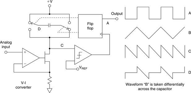
Practical VFCs of this type have linearities around 14 bits, and comparable stability, although they may be used in ADCs with higher resolutions without missing codes. The performance limits are set by comparator threshold noise, threshold temperature coefficient, and the stability and dielectric absorption (DA) of the capacitor, which is generally a discrete component. The comparator/voltage reference structure shown in the diagram is more of a representation of the function performed than the actual circuit used, which is much more integrated with the switching, and correspondingly harder to analyze.
This type of VFC is simple, inexpensive, and low powered, and most run from a wide range of supply voltages. They are ideally suited for low cost medium accuracy (12 bit) ADC and data telemetry applications.
The charge-balance VFC shown in Figure 6-76 is more complex, more demanding in its supply voltage and current requirements, and more accurate. It is capable of 16–18-bit linearity.

The integrator capacitor charges from the signal as shown in Figure 6-76. When it passes the comparator threshold, a fixed charge is removed from the capacitor, but the input current continues to flow during the discharge, so no input charge is lost. The fixed charge is defined by the precision current source and the pulse width of the precision monostable. The output pulse rate is thus accurately proportional to the rate at which the integrator charges from the input.
At low frequencies, the limits on the performance of this VFC are set by the stability of the current source and the monostable timing (which depends on the monostable capacitor, among other things). The absolute value and temperature stability of the integration capacitor do not affect the accuracy, although its leakage and dielectric absorption (DA) do. At high frequencies, second-order effects, such as switching transients in the integrator and the precision of the monostable when it is retriggered very soon after the end of a pulse, take their toll on accuracy and linearity.
The changeover switch in the current source addresses the integrator transient problem. By using a changeover switch instead of the on/off switch more common on older VFC designs: (a) there are no on/off transients in the precision current source and (b) the output stage of the integrator sees a constant load—most of the time the current from the source flows directly in the output stage; during charge balance, it still flows in the output stage, but through the integration capacitor.
The stability and transient behavior of the precision monostable present more problems, but the issue may be avoided by replacing the monostable with a clocked bistable multivibrator. This arrangement is known as a synchronous VFC or SVFC and is shown in Figure 6-77.
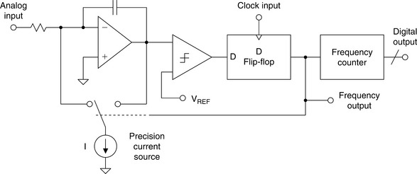
The difference from the previous circuit is quite small, but the charge-balance pulse length is now defined by two successive edges of the external clock. If this clock has low jitter, the charge will be very accurately defined. The output pulse will also be synchronous with the clock. SVFCs of this type are capable of up to 18-bit linearity and excellent temperature stability.
This synchronous behavior is convenient in many applications, since synchronous data transfer is often easier to handle than asynchronous. It does mean, however, that the output of an SVFC is not a pure tone (plus harmonics, of course) like a conventional VFC, but contains components harmonically related to the clock frequency. The display of an SVFC output on an oscilloscope is especially misleading and is a common cause of confusion—a change of input to a VFC produces a smooth change in the output frequency, but a change to an SVFC produces a change in probability density of output pulses N and N + 1 clock cycles after the previous output pulse, which is often misinterpreted as severe jitter and a sign of a faulty device (see Figure 6-78).

Another problem with SVFCs is nonlinearity at output frequencies related to the clock frequency. If we study the transfer characteristic of an SVFC, we find nonlinearities close to sub-harmonics of the clock frequency FC as shown in Figure 6-79. They can be found at FC/3, FC/4, and FC/6. This is due to stray capacitance on the chip (and in the circuit layout!) and coupling the clock signal into the SVFC comparator which causes the device to behave as an injection-locked phase-locked loop (PLL). This problem is intrinsic to SVFCs, but is not often serious: if the circuit card is well laid out, and clock amplitude and dv/dts kept as low as practical, the effect is a discontinuity in the transfer characteristic of less than 8 LSBs (at 18-bit resolution) at FC/3 and FC/4, and less at other sub-harmonics. This is frequently tolerable, since the frequencies where it occurs are known. Of course, if the circuit layout or decoupling is poor, the effect may be much larger, but this is the fault of poor design and not the SVFC itself.

It is evident that the SVFC is quantized, while the basic VFC is not. It does not follow from this that the counter/VFC ADC has higher resolution (neglecting nonlinearities) than the counter/SVFC ADC, because the clock in the counter also sets a limit to the resolution.
When a VFC has a large input, it runs quickly and (counting for a short time) gives good resolution, but it is hard to get good resolution in a reasonable sample time with a slow-running VFC. In such a case, it may be more practical to measure the period of the VFC output (this does not work for an SVFC), but of course the resolution of this system deteriorates as the input (and the frequency) increases. However, if the counter/timer arrangement is made “smart,” it is possible to measure the approximate VFC frequency and the exact period of not one, but N cycles (where the value of N is determined by the approximate frequency), and maintain high resolution over a wide range of inputs. The AD1170 modular ADC released in 1986 is an example of this architecture.
VFCs have more applications than as a component in ADCs. Since their output is a pulse stream, it may easily be sent over a wide range of transmission media (PSN, radio, optical, IR, ultrasonic, etc.). It need not be received by a counter, but by another VFC configured as a frequency-to-voltage converter (FVC). This gives an analog output, and a VFC–FVC combination is a very useful way of sending a precision analog signal across an isolation barrier.
Dual-Slope/Multi-Slope ADCs
The dual-slope ADC architecture was truly a breakthrough in ADCs for high resolution applications such as digital voltmeters (DVMs), etc. A simplified diagram is shown in Figure 6-80, and the integrator output waveforms are shown in Figure 6-81.
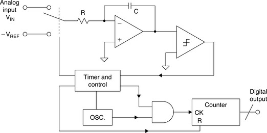
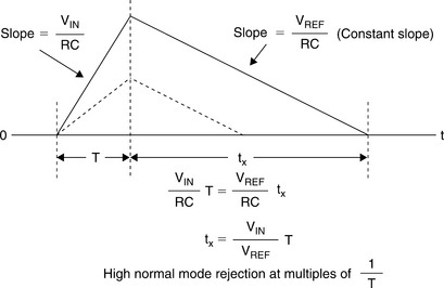
The input signal is applied to an integrator; at the same time a counter is started, counting clock pulses. After a predetermined amount of time (T), a reference voltage having opposite polarity is applied to the integrator. At that instant, the accumulated charge on the integrating capacitor is proportional to the average value of the input over the interval T. The integral of the reference is an opposite-going ramp having a slope of VREF/RC. At the same time, the counter is again counting from zero. When the integrator output reaches zero, the count is stopped, and the analog circuitry is reset. Since the charge gained is proportional to VIN × T, and the equal amount of charge lost is proportional to VREF × tx, then the number of counts relative to the full-scale count is proportional to tx/T, or VIN/VREF. If the output of the counter is a binary number, it will therefore be a binary representation of the input voltage.
Dual-slope integration has many advantages. Conversion accuracy is independent of both the capacitance and the clock frequency, because they affect both the up-slope and the down-slope by the same ratio.
The fixed input signal integration period results in rejection of noise frequencies on the analog input that have periods that are equal to or a sub-multiple of the integration time T. Proper choice of T can therefore result in excellent rejection of 50 Hz or 60 Hz line ripple as shown in Figure 6-82.

Errors caused by bias currents and the offset voltages of the integrating amplifier and the comparator as well as gain errors can be canceled by using additional charge/discharge cycles to measure “zero” and “full-scale” and using the results to digitally correct the initial measurement, as in the quad-slope architecture.
The triple-slope architecture retains the advantages of the dual-slope, but greatly increases the conversion speed at the cost of added complexity. The increase in conversion speed is achieved by accomplishing the reference integration (ramp-down) at two distinct rates: a high speed rate, and a “vernier” lower speed rate. The counter is likewise divided into two sections, one for the MSBs and one for the LSBs. In a properly designed triple-slope converter, a significant increase in speed can be achieved while retaining the inherent linearity, differential linearity, and stability characteristics associated with dual-slope ADCs.
RDCs and Synchros
Machine-tool and robotics manufacturers have increasingly turned to resolvers and synchros to provide accurate angular and rotational information. These devices excel in demanding factory applications requiring small size, long-term reliability, absolute position measurement, high accuracy, and low noise operation.
A diagram of a typical synchro and resolver is shown in Figure 6-83. Both synchros and resolvers employ single-winding rotors that revolve inside fixed stators. In the case of a simple synchro, the stator has three windings oriented 120° apart and electrically connected in a Y-connection. Resolvers differ from synchros in that their stators have only two windings oriented at 90°.

Because synchros have three stator coils in a 120° orientation, they are more difficult than resolvers to manufacture and are therefore more costly. Today, synchros find decreasing use, except in certain military and avionic retrofit applications.
Modern resolvers, in contrast, are available in a brushless form that employ a transformer to couple the rotor signals from the stator to the rotor. The primary winding of this transformer resides on the stator, and the secondary on the rotor. Other resolvers use more traditional brushes or slip rings to couple the signal into the rotor winding. Brushless resolvers are more rugged than synchros because there are no brushes to break or dislodge, and the life of a brushless resolver is limited only by its bearings. Most resolvers are specified to work over 2 V to 40 VRMS and at frequencies from 400 Hz to 10 kHz. Angular accuracies range from 5 arc-minutes to 0.5 arc-minutes. (There are 60 arc-minutes in one degree, and 60 arc-seconds in 1 arc-minute. Hence, 1 arc-minute is equal to 0.0167°.)
In operation, synchros and resolvers resemble rotating transformers. The rotor winding is excited by an AC reference voltage, at frequencies up to a few kHz. The magnitude of the voltage induced in any stator winding is proportional to the sine of the angle θ, between the rotor coil axis and the stator coil axis. In the case of a synchro, the voltage induced across any pair of stator terminals will be the vector sum of the voltages across the two connected coils.
For example, if the rotor of a synchro is excited with a reference voltage, V sin ωt, across its terminals R1 and R2, then the stator’s terminal will see voltages in the form:
where θ is the shaft angle.
In the case of a resolver, with a rotor AC reference voltage of V sin ωt, the stator’s terminal voltages will be:
It should be noted that the three-wire synchro output can be easily converted into the resolver-equivalent format using a Scott-T transformer. Therefore, the following signal processing example describes only the resolver configuration.
A typical RDC is shown functionally in Figure 6-84. The two outputs of the resolver are applied to cosine and sine multipliers. These multipliers incorporate sine and cosine lookup tables and function as multiplying DACs. Begin by assuming that the current state of the up/down counter is a digital number representing a trial angle, ϕ. The converter seeks to adjust the digital angle, ϕ, continuously to become equal to, and to track θ, the analog angle being measured. The resolver’s stator output voltages are written as:
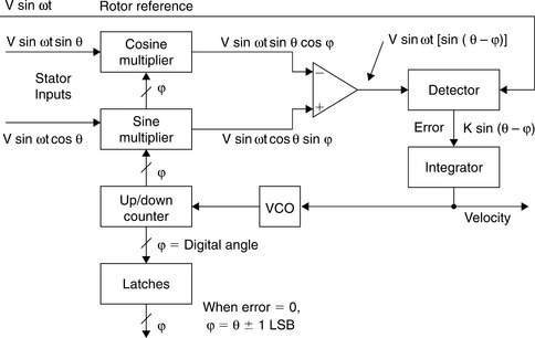
where θ is the angle of the resolver’s rotor. The digital angle ϕ is applied to the cosine multiplier, and its cosine is multiplied by V1 to produce the term:
The digital angle ϕ is also applied to the sine multiplier and multiplied by V2 to produce the term:
These two signals are subtracted from each other by the error amplifier to yield an AC error signal of the form:
Using a simple trigonometric identity, this reduces to:
The detector synchronously demodulates this AC error signal, using the resolver’s rotor voltage as a reference. This results in a DC error signal proportional to sin(θ – ϕ).
The DC error signal feeds an integrator, the output of which drives a VCO. The VCO, in turn, causes the up/down counter to count in the proper direction to cause:
and therefore
to within one count. Hence, the counter’s digital output ϕ, represents the angle θ. The latches enable this data to be transferred externally without interrupting the loop’s tracking.
This circuit is equivalent to a so-called type-2 servo loop, because it has, in effect, two integrators. One is the counter, which accumulates pulses; the other is the integrator at the output of the detector. In a type-2 servo loop with a constant rotational velocity input, the output digital word continuously follows, or tracks the input, without needing externally derived convert commands, and with no steady state phase lag between the digital output word and actual shaft angle. An error signal appears only during periods of acceleration or deceleration.
As an added bonus, the tracking RDC provides an analog DC output voltage directly proportional to the shaft’s rotational velocity. This is a useful feature if velocity is to be measured or used as a stabilization term in a servo system, and it makes tachometers unnecessary.
Since the operation of an RDC depends only on the ratio between input signal amplitudes, attenuation in the lines connecting them to resolvers does not substantially affect performance. For similar reasons, these converters are not greatly susceptible to waveform distortion. In fact, they can operate with as much as 10% harmonic distortion on the input signals; some applications actually use square-wave references with little additional error.
Tracking ADCs are therefore ideally suited to RDCs. While other ADC architectures, such as successive approximation, could be used, the tracking converter is the most accurate and efficient for this application. Because the tracking converter doubly integrates its error signal, the device offers a high degree of noise immunity (12 dB/octave rolloff). The net area under any given noise spike produces an error. However, typical inductively coupled noise spikes have equal positive and negative-going waveforms. When integrated, this results in a zero net error signal. The resulting noise immunity, combined with the converter’s insensitivity to voltage drops, lets the user locate the converter at a considerable distance from the resolver. Noise rejection is further enhanced by the detector’s rejection of any signal not at the reference frequency, such as wideband noise.
The AD2S90 is one of a number of integrated RDCs offered by Analog Devices. The general architecture is similar to that of Figure 6-83. Further details on synchro and RDCs can be found in the references. Syncros and resolvers are also discussed in Chapter 3 (Section 3-1).
1 W. Kester, Editor, Amplifier Applications Guide, Analog Devices, 1992, ISBN-0-916550-10-9, Chapter 10. (An excellent discussion by James Bryant on the use of op amps as comparators.)
2 J.N. Giles, “High Speed Transistor Difference Amplifier,” US Patent 3,843,934, filed, January 31, 1973, issued October 22, 1974. (Describes one of the first high-speed ECL comparators, the AM685.)
3 Mangelsdorf C.W. A 400-MHz Input Flash Converter with Error Correction. IEEE Journal of Solid-State Circuits. 1990;Vol. 25(1):184–191. February (A discussion of the AD770, an 8-bit 200 MSPS flash ADC. The paper describes the comparator metastable state problem and how to optimize the ADC design to minimize its effects.)
4 Woodward C.E. A Monolithic Voltage-Comparator Array for A/D Converters. IEEE Journal of Solid State Circuits. 1975;Vol. SC-10(6):392–399. December, (An early paper on a 3-bit flash converter optimized to minimize metastable state errors.)
5 P.M. Rainey, “Facsimile Telegraph System,” US Patent 1,608,527, filed, July 20, 1921, issued November 30, 1926. (Although A.H. Reeves is generally credited with the invention of PCM, this patent discloses an electro-mechanical PCM system complete with A/D and D/A converters. The 5-bit electro-mechanical ADC described is probably the first documented flash converter. The patent was largely ignored and forgotten until many years after the various Reeves’ patents were issued in 1939–1942.)
6 Sears R.W. Electron Beam Deflection Tube for Pulse Code Modulation. Bell System Technical Journal. 1948;Vol. 27:44–57. January (Describes an electron-beam deflection tube 7-bit, 100-kSPS flash converter for early experimental PCM work.)
7 F. Gray, “Pulse Code Communication,” US Patent 2,632,058, filed, November 13, 1947, issued March 17, 1953. (Detailed patent on the Gray code and its application to electron beam coders.)
8 Edson J.O., Henning H.H. Broadband Codecs for an Experimental 224 Mb/s PCM Terminal. Bell System Technical Journal. 1965;Vol. 44:1887–1940. November (Summarizes experiments on ADCs based on the electron tube coder as well as a bit-per-stage Gray code 9-bit solid state ADC. The electron beam coder was 9-bits at 12 MSPS, and represented the fastest of its type at the time.)
9 R. Staffin and R.D. Lohman, “Signal Amplitude Quantizer,” US Patent 2,869,079, filed, December 19, 1956, issued January 13, 1959. (Describes flash and subranging conversion using tubes and transistors.)
10 Goto E., et al. Esaki Diode High-Speed Logical Circuits. IRE Transactions on Electronic Computers. 1960;Vol. EC-9:25–29. March (Describes how to use tunnel diodes as logic elements.)
11 Kiyomo T., Ikeda K., Ichiki H. Analog-to-Digital Converter Using an Esaki Diode Stack. IRE Transactions on Electronic Computers. 1962;Vol. EC-11:791–792. December (Description of a low resolution 3-bit flash ADC using a stack of tunnel diodes.)
12 H.R. Schindler, “Using the Latest Semiconductor Circuits in a UHF Digital Converter,” Electronics, August, 1963, pp. 37–40. (Describes a 6-bit 50-MSPS subranging ADC using three 2-bit tunnel diode flash converters.)
13 Earnshaw J.B. Design for a Tunnel Diode-Transistor Store with Nondestructive Read-out of Information. IEEE Transactions on Electronic Computers. 1964;Vol. EC-13:710–722. (Use of tunnel diodes as memory elements.)
14 Bucklen W.K. A Monolithic Video A/D Converter. In: Digital Video, Vol. 2. March: Society of Motion Picture and Television Engineers; 1979:34–42. (Describes the revolutionary TDC1007J 8-bit 20 MSPS video flash converter. Originally introduced at the February 3, 1979, SMPTE Winter Conference in San Francisco, Bucklen accepted an Emmy award for this product in 1988 and was responsible for the initial marketing and applications support for the device.)
15 Peterson J. A Monolithic Video A/D Converter. IEEE Journal of Solid-State Circuits. 1979;Vol. SC-14(6):932–937. December, (Another detailed description of the TRW TDC1007J 8-bit, 20-MSPS flash converter.)
16 Y. Akazawa et. al., A 400 MSPS 8 Bit Flash A/D Converter. 1987 ISSCC Digest of Technical Papers, pp. 98–99. (Describes a monolithic flash converter using Gray decoding.)
17 Matsuzawa et al., An 8b 600 MHz Flash A/D Converter with Multi-stage Duplex-gray Coding. Symposium VLSI Circuits, Digest of Technical Papers, May, 1991, pp. 113–114. (Describes a monolithic flash converter using Gray decoding.)
18 Chuck Lane, A 10-bit 60 MSPS Flash ADC. Proceedings of the 1989 Bipolar Circuits and Technology Meeting, IEEE Catalog No. 89CH2771-4, September, 1989, pp. 44–47. (Describes an interpolating method for reducing the number of preamps required in a flash converter.)
19 W.W. Rouse Ball and H.S.M. Coxeter, Mathematical Recreations and Essays, 13th Edition, Dover Publications, 1987, pp. 50, 51. (Describes a mathematical puzzle for measuring unknown weights using the minimum number of weighing operations. The solution proposed in the 500’s is the same basic successive approximation algorithm used today.)
20 A.H. Reeves, “Electric Signaling System,” US Patent 2,272,070, filed, November 22, 1939, issued February 3, 1942. Also French Patent 852,183 issued 1938, and British Patent 538,860 issued 1939. (The ground-breaking patent on PCM. Interestingly enough, the ADC and DAC proposed by Reeves are counting types, and not successive approximation.)
21 J.C. Schelleng, “Code Modulation Communication System,” US Patent 2,453,461, filed, June 19, 1946, issued November 9, 1948. (An interesting description of a rather cumbersome successive approximation ADC based on vacuum tube technology. This converter was not very practical, but did illustrate the concept. Also in the patent is a description of a corresponding binary DAC.)
22 Goodall W.M. Telephony by Pulse Code Modulation. Bell System Technical Journal. 1947;Vol. 26:395–409. July (Describes an experimental PCM system using a 5-bit, 8 KSPS successive approximation ADC based on the subtraction of binary weighted charges from a capacitor to implement the internal subtraction/DAC function. It required 5 internal reference voltages.)
23 H.R. Kaiser, et al., “High-Speed Electronic Analogue-to-Digital Converter System,” US Patent 2,784,396, filed, April 2, 1953, issued March 5, 1957. (One of the first SAR ADCs to use an actual binary-weighted DAC internally.)
24 Smith B.D. Coding by Feedback Methods. Proceedings of the IRE. 1953;Vol. 41:1053–1058. August (Smith uses an internal DAC and also points out that a non-linear transfer function can be achieved by using a DAC with non-uniform bit weights, a technique which is widely used in today’s voiceband ADCs with built-in companding.)
25 Meacham L.A., Peterson E. An Experimental Multichannel Pulse Code Modulation System of Toll Quality. Bell System Technical Journal. 1948;Vol. 27(1):1–43. January, (Describes non-linear diode-based compressors and expanders for generating a non-linear ADC/DAC transfer function.)
26 B.M. Gordon and R.P. Talambiras, “Signal Conversion Apparatus,” US Patent 3,108,266, filed, July 22, 1955, issued October 22, 1963. (Classic patent describing Gordon’s 11-bit, 20 kSPS vacuum tube successive approximation ADC done at Epsco. The internal DAC represents the first known use of equal currents switched into an R/2R ladder network.)
27 B.M. Gordon and E.T. Colton, “Signal Conversion Apparatus,” US Patent 2,997,704, filed, February 24, 1958, issued August 22, 1961. (Classic patent describes the logic to perform the successive approximation algorithm in an SAR ADC.)
28 Gray J.R., Kitsopoulos S.C. A Precision Sample-and-Hold Circuit with Subnanosecond Switching. IEEE Transactions on Circuit Theory. 1964;Vol. CT11:389–396. September (One of the first papers on the detailed analysis of a sample-and-hold circuit.)
29 Verster T.C. A Method to Increase the Accuracy of Fast Serial-Parallel Analog-to-Digital Converters. IEEE Transactions on Electronic Computers. 1964;Vol. EC-13:471–473. (One of the first references to the use of error correction in a subranging ADC.)
30 G.G. Gorbatenko, “High-Performance Parallel-Serial Analog to Digital Converter with Error Correction,” IEEE National Convention Record, New York, March, 1966. (Another early reference to the use of error correction in a subranging ADC.)
31 Kinniment D.J., Aspinall D., Edwards D.B.G. High-Speed Analogue-Digital Converter. IEE Proceedings. 1966;Vol. 113:2061–2069. December (A 7-bit 9 MSPS three-stage pipelined error corrected converter is described based on recirculating through a 3-bit stage three times. Tunnel (Esaki) diodes are used for the individual comparators. The article also shows a proposed faster pipelined 7-bit architecture using three individual 3-bit stages with error correction. The article also describes a fast bootstrapped diode-bridge sample-and-hold circuit.)
32 Horna O.A. A 150 Mbps A/D and D/A Conversion System. Comsat Technical Review. 1972;Vol. 2(1):52–57. (A detailed description and analysis of a subranging ADC with error correction.)
33 J.L. Fraschilla, R.D. Caveney, and R.M. Harrison, “High Speed Analog-to-Digital Converter,” US Patent 3,597,761, filed, November 14, 1969, issued August 13, 1971. (Describes an 8-bit, 5-MSPS subranging ADC with switched references to second comparator bank.)
34 Lewis S.H., Fetterman S., Gross G.F., Jr., Ramachandran R., Viswanathan T.R. A 10-b 20-Msample/s Analog-Digital Converter. IEEE Journal of Solid-State Circuits. 1992;Vol. 27(3):351–358. March, (A detailed description and analysis of an error corrected subranging ADC using 1.5-bit pipelined stages.)
35 R. Gosser and F. Murden, “A 12-bit 50 MSPS Two-Stage A/D Converter,” 1995 ISSCC Digest of Technical Papers, p. 278. (A description of the AD9042 error corrected subranging ADC using MagAMP stages for the internal ADCs.)
36 B.D. Smith, “An Unusual Electronic Analog-Digital Conversion Method,” IRE Transactions on Instrumentation, June, 1956, pp. 155–160. (Possibly the first published description of the binary-coded and Gray-coded bit-per-stage ADC architectures. Smith mentions similar work partially covered in R. P. Sallen’s 1949 thesis at M.I.T.)
37 N.E. Chasek, “Pulse Code Modulation Encoder,” US Patent 3,035,258, filed, November 14, 1960, issued May 15, 1962. (An early patent showing a diode-based circuit for realizing the Gray code folding transfer function.)
38 F.D. Waldhauer, “Analog-to-Digital Converter,” US Patent 3,187,325, filed, July 2, 1962, issued June 1, 1965. (A classic patent using op amps with diode switches in the feedback loops to implement the Gray code folding transfer function.)
39 Edson J.O., Henning H.H. Broadband Codecs for an Experimental 224 Mb/s PCM Terminal. Bell System Technical Journal. 1965;Vol. 44:1887–1940. November (A further description of a 9-bit ADC based on Waldhauer’s folding stage.)
40 Fiedler U., Seitzer D. A High-Speed 8 Bit A/D Converter Based on a Gray-Code Multiple Folding Circuit. IEEE Journal of Solid-State Circuits. 1979;Vol. SC-14(3):547–551. June, (An early monolithic folding ADC.)
41 van de Plassche R.J., van der Grift R.E.J. A High-Speed 7 Bit A/D Converter. IEEE Journal of Solid-State Circuits. 1979;Vol. SC-14(6):938–943. December, (A monolithic folding ADC.)
42 van de Grift R.E.J., van der Plassche R.J. A Monolithic 8-bit Video A/D Converter. IEEE Journal of Solid State Circuits. 1984;Vol. SC-19(3):374–378. June, (A monolithic folding ADC.)
43 van der Grift R.E.J., Rutten I.W.J.M., van der Veen M. An 8-bit Video ADC Incorporating Folding and Interpolation Techniques. IEEE Journal of Solid State Circuits. 1987;Vol. SC-22(6):944–953. December, (Another monolithic folding ADC.)
44 van de Plassche R. Integrated Analog-to-Digital and Digital-to-Analog Converters. Norwell, Ma.: Kluwer Academic Publishers, 1994;148–187. (A good textbook on ADCs and DACs with a section on folding ADCs indicated by the referenced page numbers.)
45 C. Moreland, “An 8-bit 150 MSPS Serial ADC,” 1995 ISSCC Digest of Technical Papers, Vol. 38, p. 272. (A description of an 8-bit ADC with 5 folding stages followed by a 3-bit flash converter.)
46 C. Moreland, An Analog-to-Digital Converter Using Serial-Ripple Architecture, Masters’ Thesis, Florida State University College of Engineering, Department of Electrical Engineering, 1995. (Moreland’s early work on folding ADCs.)
47 F. Murden, “Analog to Digital Converter Using Complementary Differential Emitter Pairs,” US Patent 5,550,492, filed, December 1, 1994, issued August 27, 1996. (A description of an ADC based on the MagAMP folding stage.)
48 C.W. Moreland, “Analog to Digital Converter Having a Magnitude Amplifier with an Improved Differential Input Amplifier,” US Patent 5,554,943, filed, December 1, 1994, issued September 10, 1996. (A. description of an 8-bit ADC with 5 folding stages followed by a 3-bit flash converter.)
49 F. Murden and C.W. Moreland, “N-bit Analog-to-Digital Converter with N-1 Magnitude Amplifiers and N Comparators,” US Patent 5,684,419, filed, December 1, 1994, issued November 4, 1997. (Another patent on the MagAMP folding architecture applied to an ADC.)
50 Moreland C., Murden F., Elliott M., Young J., Hensley M., Stop R. A 14-bit 100-Msample/s Subranging ADC. IEEE Journal of Solid State Circuits. 2000;Vol. 35(12):1791–1798. December, (Describes the architecture used in the 14-bit AD6645 ADC.)
51 F. Murden and M.R. Elliott, “Linearizing Structures and Methods for Adjustable-Gain Folding Amplifiers,” US Patent 6,172,636B1, filed, July 13, 1999, issued January 9, 2001. (Describes methods for trimming the folding amplifiers in an ADC.)
52 B.M. Oliver and C.E. Shannon, “Communication System Employing Pulse Code Modulation,” US Patent 2,801,281, filed, February 21, 1946, issued July 30, 1957. (Charge run-down ADC and Shannon-Rack DAC.)
53 A.H. Dickinson, “Device to Manifest an Unknown Voltage as a Numerical Quantity,” US. Patent 2,872,670, filed, May 26, 1951, issued February 3, 1959. (Ramp run-up ADC.)
54 K. Howard Barney, “Binary Quantizer,” US Patent 2,715,678, filed, May 26, 1950, issued August 16, 1955. (Tracking ADC.)
55 B.M. Gordon and R.P. Talambiras, “Information Translating Apparatus and Method,” US Patent 2,989,741, filed, July 22, 1955, issued June 20, 1961. (Tracking ADC.)
56 J.L. Lindesmith, “Voltage-to-Digital Measuring Circuit,” US Patent 2,835,868, filed, September 16, 1952, issued May 20, 1958. (Voltage-to-frequency ADC.)
57 P. Klonowski, “Analog-to-Digital Conversion Using Voltage-to-Frequency Converters,” Application Note AN-276, Analog Devices, Inc. (A good application note on VFCs.) Norwood, Ma.
58 P. Klonowski, “Analog-to-Digital Conversion Using Voltage-to-Frequency Converters,” Application Note AN-276, Analog Devices, Inc. (A good application note on VFCs.) Norwood, Ma
59 W. Jung, “Operation and Applications of the AD654 IC V-F Converter,” Application Note AN-278, Analog Devices, Inc., Norwood, Ma
60 S. Martin, “Using the AD650 Voltage-to-Frequency Converter as a Frequency-to-Voltage Converter,” Application Note AN-279, Analog Devices, Inc. (A. description of a frequency-to-voltage converter using the popular AD650 VFC.) Norwood, Ma.
61 R.N. Anderson and H.A. Dorey, “Digital Voltmeters,” US Patent 3,267,458, filed, August 20, 1962, issued August 16, 1966. (Charge balance dual slope voltmeter ADC.)
62 R. Olshausen, “Analog-to-Digital Converter,” US Patent 3,281,827, filed, June 27, 1963, issued October 25, 1966. (Charge balance dual slope ADC.)
63 R.W. Gilbert, “Analog-to-Digital Converter,” US Patent 3,051,939, filed, May 8, 1957, issued August 28, 1962. (Dual-slope ADC.)
64 S.K. Ammann, “Integrating Analog-to-Digital Converter,” US Patent 3,316,547, filed, July 15, 1964, issued April 25, 1967. (Dual-slope ADC.)
65 I. Wold, “Integrating Analog-to-Digital Converter Having Digitally Derived Offset Error Compensation and Bipolar Operation without Zero Discontinuity,” US Patent 3,872,466, filed, July 19, 1973, issued March 18, 1975. (Quad-slope ADC.)
66 H.B. Aasnaes, “Triple Integrating Ramp Analog-to-Digital Converter,” US Patent 3,577,140, filed, June 27, 1967, issued May 4, 1971. (Triple-slope ADC.)
67 F. Bondzeit, L.J. Neelands, “Multiple Slope Analog-to-Digital Converter,” US Patent 3,564,538, filed, January 29, 1968, issued February 16, 1971. (Triple-slope ADC.)
68 D. Wheable, “Triple-Slope Analog-to-Digital Converters,” US Patent 3,678,506, filed, October 2, 1968, issued July 18, 1972. (Triple-slope ADC.)
69 D. Sheingold, Analog-Digital Conversion Handbook, Prentice-Hall, Norwood, Ma., 1986, ISBN-0-13-032848-0, pp. 441–471. (This chapter contains an excellent tutorial on optical, synchro, and resolver-to-digital conversion.)
70 Dennis Fu, “Circuit Applications of the AD2S90 Resolver-to-Digital Converter,” Application Note AN-230, Analog Devices. (Applications of the AD2S90 RTD.) Norwood, Ma.
SECTION 6-3 Sigma–Delta Converters
Historical Perspective
The sigma–delta (Σ–Δ) ADC architecture had its origins in the early development phases of PCM systems—specifically, those related to transmission techniques called delta modulation and differential PCM. (An excellent discussion of both the history and concepts of the sigma–delta ADC can be found by Max Hauser in Reference 1).
The driving force behind delta modulation and differential PCM was to achieve higher transmission efficiency by transmitting the changes (delta) in value between consecutive samples rather than the actual samples themselves.
In delta modulation, the analog signal is quantized by a 1-bit ADC (a comparator) as shown in Figure 6-85(A). The comparator output is converted back to an analog signal with a 1-bit DAC, and subtracted from the input after passing through an integrator. The shape of the analog signal is transmitted as follows: a “1” indicates that a positive excursion has occurred since the last sample, and a “0” indicates that a negative excursion has occurred since the last sample.
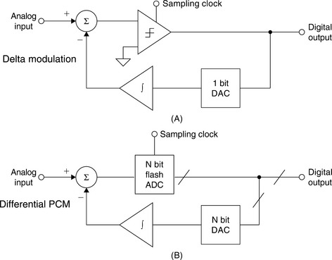
If the analog signal remains at a fixed DC level for a period of time, a pattern alternating of “0s” and “1s” is obtained. It should be noted that differential PCM (see Figure 6-85(B)) uses exactly the same concept except a multibit ADC is used rather than a comparator to derive the transmitted information.
Since there is no limit to the number of pulses of the same sign that may occur, delta modulation systems are capable of tracking signals of any amplitude. In theory, there is no peak clipping. However, the theoretical limitation of delta modulation is that the analog signal must not change too rapidly. The problem of slope clipping is shown in Figure 6-86. Here, although each sampling instant indicates a positive excursion, the analog signal is rising too quickly, and the quantizer is unable to keep pace.

Slope clipping can be reduced by increasing the quantum step size or increasing the sampling rate. Differential PCM uses a multibit quantizer to effectively increase the quantum step sizes at the increase of complexity. Tests have shown that in order to obtain the same quality as classical PCM, delta modulation requires very high sampling rates, typically 20 times the highest frequency of interest, as opposed to Nyquist rate of 2 times.
For these reasons, delta modulation and differential PCM have never achieved any significant degree of popularity, however a slight modification of the delta modulator leads to the basic sigma–delta architecture, one of the most popular high resolution ADC architectures in use today.
The basic single and multibit first-order sigma–delta ADC architecture is shown in Figure 6-87(A) and 6-87(B), respectively. Note that the integrator operates on the error signal, whereas in a delta modulator, the integrator is in the feedback loop. The basic oversampling sigma–delta modulator increases the overall SNR at low frequencies by shaping the quantization noise such that most of it occurs outside the bandwidth of interest. The digital filter then removes the noise outside the bandwidth of interest, and the decimator reduces the output data rate back to the Nyquist rate.

The IC sigma–delta ADC offers several advantages over the other architectures, especially for high resolution, low frequency applications. First and foremost, the single-bit sigma–delta ADC is inherently monotonic and requires no laser trimming. The sigma–delta ADC also lends itself to low cost foundry CMOS processes because of the digitally intensive nature of the architecture. Examples of early monolithic sigma–delta ADCs are given in References 13–21. Since that time there have been a constant stream of process and design improvements in the fundamental architecture proposed in the early works cited above.
Sigma–Delta, (Σ–Δ), or Delta–Sigma, (Δ–Σ)?, Editor’s Notes from, Analog Dialogue Vol. 24-2, 1990, by Dan Sheingold
This is not the most earth-shaking of controversies, and many readers may wonder what the fuss is all about—if they wonder at all. The issue is important to both editor and readers because of the need for consistency; we would like to use the same name for the same thing whenever it appears. But which name? In the case of the modulation technique that led to a new oversampling A/D conversion mechanism, we chose sigma–delta. Here is why.
Ordinarily, when a new concept is named by its creators, the name sticks; it should not be changed unless it is erroneous or flies in the face of precedent. The seminal paper on this subject was published in 1962 (References 9, 10), and its authors chose the name “delta–sigma modulation,” since it was based on delta modulation but included an integration (summation, hence Σ).
Delta–sigma was apparently unchallenged until the 1970s, when engineers at AT&T were publishing papers using the term sigma–delta. Why? According to Hauser (Reference 1), the precedent had been to name variants of delta modulation with adjectives preceding the word “delta.” Since the form of modulation in question is a variant of delta modulation, the sigma, used as an adjective—so the argument went—should precede the delta.
Many engineers who came upon the scene subsequently used whatever term caught their fancy, often without knowing why. It was even possible to find both terms used interchangeably in the same paper. As matters stand today, sigma–delta is in widespread use, probably for the majority of citations. Would its adoption be an injustice to the inventors of the technique?
We think not. Like others, we believe that the name delta–sigma is a departure from precedent. Not just in the sense of grammar, but also in relation to the hierarchy of operations. Consider a block diagram for embodying an analog root mean square (RMS) (finding the square root of the mean of a squared signal) computer. First the signal is squared, then it is integrated, and finally it is rooted (see Figure 6-88).

If we were to name the overall function after the causal order of operations, it would have to be called a “square mean root” function. But naming in order of the hierarchy of its mathematical operations gives us the familiar—and undisputed—name, root mean square. Consider now a block diagram for taking a difference (delta), and then integrating it (sigma).
Its causal order would give delta–sigma, but in functional hierarchy it is sigma–delta, since it computes the integral of a difference. We believe that the latter term is correct and follows precedent; and we have adopted it as our standard.
Basics of Sigma–Delta ADCs
Sigma–delta analog-to-digital converters (Σ–Δ ADCs) have been known for over 30 years, but only recently has the technology (high density digital VLSI) existed to manufacture them as inexpensive monolithic ICs. They are now used in many applications where a low cost, low bandwidth, low power, high resolution ADC is required.
There have been innumerable descriptions of the architecture and theory of Σ–Δ ADCs, but most commence with a maze of integrals and deteriorate from there. (Some engineers who do not understand the theory of operation of Σ–Δ ADCs and are convinced, from study of a typical published article, which it is too complex to comprehend easily.)
There is nothing particularly difficult to understand about Σ–Δ ADCs, as long as you avoid the detailed mathematics, and this section has been written in an attempt to clarify the subject. A Σ–Δ ADC contains very simple analog electronics (a comparator, voltage reference, a switch, and one or more integrators and analog summing circuits), and quite complex digital computational circuitry. This circuitry consists of a digital signal processor (DSP) which acts as a filter (generally, but not invariably, a lowpass filter (LPF)). It is not necessary to know precisely how the filter works to appreciate what it does. To understand how a Σ–Δ ADC works, familiarity with the concepts of oversampling, quantization noise shaping, digital filtering, and decimation is required.
Let us consider the technique of oversampling with an analysis in the frequency domain. Where a DC conversion has a quantization error of up to ½ LSB, a sampled data system has quantization noise.
A perfect classical N-bit sampling ADC has an RMS quantization noise of q/√12 uniformly distributed within the Nyquist band of DC to fs/2 (where q is the value of an LSB and fs is the sampling rate) as shown in Figure 6-89(A). Therefore, its SNR with a full-scale sinewave input will be (6.02 N + 1.76) dB. If the ADC is less than perfect, and its noise is greater than its theoretical minimum quantization noise, then its effective resolution will be less than N-bits. Its actual resolution (often known as its effective number of bits or ENOB) will be defined by:

If we choose a much higher sampling rate, Kfs (see Figure 6-89(B)), the RMS quantization noise remains ![]() , but the noise is now distributed over a wider bandwidth DC to Kfs/2. If we then apply a digital LPF to the output, we remove much of the quantization noise, but do not affect the wanted signal—so the ENOB is improved. We have accomplished a high resolution A/D conversion with a low resolution ADC. The factor K is generally referred to as the oversampling ratio. It should be noted at this point that oversampling has an added benefit in that it relaxes the requirements on the analog antialiasing filter.
, but the noise is now distributed over a wider bandwidth DC to Kfs/2. If we then apply a digital LPF to the output, we remove much of the quantization noise, but do not affect the wanted signal—so the ENOB is improved. We have accomplished a high resolution A/D conversion with a low resolution ADC. The factor K is generally referred to as the oversampling ratio. It should be noted at this point that oversampling has an added benefit in that it relaxes the requirements on the analog antialiasing filter.
Since the bandwidth is reduced by the digital output filter, the output data rate may be lower than the original sampling rate (Kfs) and still satisfy the Nyquist criterion. This may be achieved by passing every Mth result to the output and discarding the remainder. The process is known as “decimation” by a factor of M. Despite the origins of the term (decem is Latin for 10), M can have any integer value, provided that the output data rate is more than twice the signal bandwidth. Decimation does not cause any loss of information (see Figure 6-89(B)).
If we simply use oversampling to improve resolution, we must oversample by a factor of 22N to obtain an N-bit increase in resolution. The Σ–Δ converter does not need such a high oversampling ratio because it not only limits the signal passband, but also shapes the quantization noise so that most of it falls outside this passband as shown in Figure 6-89(C).
If we take a 1-bit ADC (generally known as a comparator), drive it with the output of an integrator, and feed the integrator with an input signal summed with the output of a 1-bit DAC fed from the ADC output, we have a first-order Σ–Δ modulator as shown in Figure 6-90. Add a digital LPF and decimator at the digital output, and we have a Σ–Δ ADC—the Σ–Δ modulator shapes the quantization noise so that it lies above the passband of the digital output filter, and the ENOB is therefore much larger than would otherwise be expected from the oversampling ratio.

Intuitively, a Σ–Δ ADC operates as follows. Assume a DC input at VIN. The integrator is constantly ramping up or down at node A. The output of the comparator is fed back through a 1-bit DAC to the summing input at node B. The negative feedback loop from the comparator output through the 1-bit DAC back to the summing point will force the average DC voltage at node B to be equal to VIN. This implies that the average DAC output voltage must be equal to the input voltage VIN. The average DAC output voltage is controlled by the ones-density in the 1-bit data stream from the comparator output. As the input signal increases toward + VREF, the number of “ones” in the serial bit stream increases, and the number of “zeros” decreases. Similarly, as the signal goes negative toward –VREF, the number of “ones” in the serial bit stream decreases, and the number of “zeros” increases. From a very simplistic standpoint, this analysis shows that the average value of the input voltage is contained in the serial bit stream out of the comparator. The digital filter and decimator process the serial bit stream and produce the final output data.
For any given input value in a single sampling interval, the data from the 1-bit ADC is virtually meaningless. Only when a large number of samples are averaged will a meaningful value result. The sigma–delta modulator is very difficult to analyze in the time domain because of this apparent randomness of the single-bit data output. If the input signal is near positive full-scale, it is clear that there will be more 1 second than 0 second in the bit stream. Likewise, for signals near negative full-scale, there will be more 0 second than 1 second in the bit stream. For signals near mid-scale, there will be approximately an equal number of 1 second and 0 second. Figure 6-91 shows the output of the integrator for two input conditions. The first is for an input of zero (mid-scale). To decode the output, pass the output samples through a simple digital LPF that averages every four samples. The output of the filter is 2/4. This value represents bipolar zero. If more samples are averaged, more dynamic range is achieved. For example, averaging 4 samples gives 2 bits of resolution, while averaging 8 samples yields 4/8, or 3 bits of resolution. In the bottom waveform of Figure 6-91, the average obtained for 4 samples is 3/4, and the average for 8 samples is 6/8.
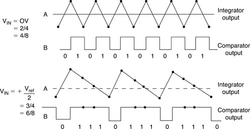
Further time-domain analysis is not productive, and the concept of noise shaping is best explained in the frequency domain by considering the simple Σ–Δ modulator model in Figure 6-92.

The integrator in the modulator is represented as an analog LPF with a transfer function equal to H(f) = 1/f. This transfer function has an amplitude response which is inversely proportional to the input frequency. The 1-bit quantizer generates quantization noise, Q, which is injected into the output summing block. If we let the input signal be X, and the output Y, the signal coming out of the input summer must be X – Y. This is multiplied by the filter transfer function, 1/f, and the result goes to one input to the output summer. By inspection, we can then write the expression for the output voltage Y as:
This expression can easily be rearranged and solved for Y in terms of X, f, and Q:
Note that as the frequency f approaches zero, the output voltage Y approaches X with no noise component. At higher frequencies, the amplitude of the signal component approaches zero, and the noise component approaches Q. At high frequency, the output consists primarily of quantization noise. In essence, the analog filter has a lowpass effect on the signal, and a highpass effect on the quantization noise. Thus the analog filter performs the noise shaping function in the Σ–Δ modulator model.
For a given input frequency, higher order analog filters offer more attenuation. The same is true of Σ–Δ modulators, provided certain precautions are taken.
By using more than one integration and summing stage in the Σ–Δ modulator, we can achieve higher orders of quantization noise shaping and even better ENOB for a given oversampling ratio as is shown in Figure 6-93 for both a first- and second-order Σ–Δ modulator.

The block diagram for the second-order Σ–Δ modulator is shown in Figure 6-94. Third, and higher, order Σ–Δ ADCs were once thought to be potentially unstable at some values of input—recent analyses using finite rather than infinite gains in the comparator have shown that this is not necessarily so, but even if instability does start to occur, it is not important, since the DSP in the digital filter and decimator can be made to recognize incipient instability and react to prevent it.

Figure 6-95 shows the relationship between the order of the Σ–Δ modulator and the amount of oversampling necessary to achieve a particular SNR. For instance, if the oversampling ratio is 64, an ideal second-order system is capable of providing an SNR of about 80 dB. This implies approximately 13 ENOB. Although the filtering done by the digital filter and decimator can be done to any degree of precision desirable, it would be pointless to carry more than 13 binary bits to the outside world. Additional bits would carry no useful signal information, and would be buried in the quantization noise unless post-filtering techniques were employed. Additional resolution can be obtained by increasing the oversampling ratio and/or by using a higher order modulator.

Idle-Tone Considerations
In our discussion of sigma–delta ADCs up to this point, we have made the assumption that the quantization noise produced by the sigma–delta modulator is random and uncorrelated with the input signal. Unfortunately, this is not entirely the case, especially for the first-order modulator. Consider the case where we are averaging 16 samples of the modulator output in a 4-bit sigma–delta ADC.
Figure 6-96 shows the bit pattern for two input signal conditions: an input signal having the value 8/16, and an input signal having the value 9/16. In the case of the 9/16 signal, the modulator output bit pattern has an extra “1” every 16th output. This will produce energy at fs/16, which translates into an unwanted tone. If the oversampling ratio is less than 16, this tone will fall into the passband. In audio applications these tones are referred to as “idle tones.”

Figure 6-97 shows the correlated idling pattern behavior for a first-order sigma–delta modulator, and Figure 6-98 shows the relatively uncorrelated pattern for a second-order modulator. For this reason, virtually all sigma–delta ADCs contain at least a second-order modulator loop.


Higher Order Loop Considerations
In order to achieve wide dynamic range, sigma–delta modulator loops greater than second-order are necessary, but present real design challenges. First of all, the simple linear models previously discussed are no longer fully accurate. Loops of order greater than two are generally not guaranteed to be stable under all input conditions. The instability arises because the comparator is a nonlinear element whose effective “gain” varies inversely with the input level. This mechanism for instability causes the following behavior: if the loop is operating normally, and a large signal is applied to the input that overloads the loop, the average gain of the comparator is reduced. The reduction in comparator gain in the linear model causes loop instability. This causes instability even when the signal that caused it is removed. In actual practice, such a circuit would normally oscillate on power-up due to initial conditions caused by turn-on transients. As an example, the AD1879 dual audio ADC released in 1994 by Analog Devices used a fifth-order loop. Extensive nonlinear stabilization techniques were required in this and similar higher order loop designs (References 22–26).
MultiBit Sigma–Delta Converters
So far we have considered only sigma–delta converters which contain a single-bit ADC (comparator) and a single-bit DAC (switch). The block diagram of Figure 6-99 shows a multibit sigma–delta ADC which uses an n-bit flash ADC and an n-bit DAC. Obviously, this architecture will give a higher dynamic range for a given oversampling ratio and order of loop filter. Stabilization is easier, since second-order loops can generally be used. Idling patterns tend to be more random thereby minimizing tonal effects.
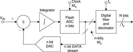
The real disadvantage of this technique is that the linearity depends on the DAC linearity, and thin-film laser trimming is required to approach 16-bit performance levels. This makes the multibit architecture extremely impractical to implement on mixed-signal ICs using traditional binary DAC techniques.
However, fully decoded thermometer DACs coupled with proprietary data scrambling techniques as used in a number of Analog Devices’ audio ADCs and DACs, including the 24-bit stereo AD1871 (see References 27 and 28) can achieve high SNR and low distortion using the multibit architecture. A simplified block diagram of the AD1871 ADC is shown in Figure 6-100.

The AD1871’s analog Σ–Δ modulator section comprises a second-order multibit implementation using Analog Device’s proprietary technology for best performance. As shown in Figure 6-101, the two analog integrator blocks are followed by a flash ADC section that generates the multibit samples.

The output of the flash ADC, which is thermometer encoded, is decoded to binary for output to the filter sections and is scrambled for feedback to the two integrator stages. The modulator is optimized for operation at a sampling rate of 6.144 MHz (which is 128 × fs at 48 kHz sampling and 64 × fs at 96 kHz sampling). The A-weighted dynamic range of the AD1871 is typically 105 dB.
Digital Filter Implications
The digital filter is an integral part of all sigma–delta ADCs—there is no way to remove it. The settling time of this filter affects certain applications especially when using sigma–delta ADCs in multiplexed applications. The output of a multiplexer can present a step function input to an ADC if there are different input voltages on adjacent channels. In fact, the multiplexer output can represent a full-scale step voltage to the sigma–delta ADC when channels are switched. Adequate filter settling time must be allowed, therefore, in such applications. This does not mean that sigma–delta ADCs should not be used in multiplexed applications, just that the settling time of the digital filter must be considered. Some newer sigma–delta ADCs are actually optimized for use in multiplexed applications.
For example, the group delay through the AD1871 digital filter is 910 μs (sampling at 48 kSPS) and 460 μs (sampling at 96 kSPS)—this represents the time it takes for a step function input to propagate through one-half the number of taps in the digital filter. The total settling time is therefore approximately twice the group delay time. The input oversampling frequency is 6.144 MSPS for both conditions. The frequency response of the digital filter in the AD1871 ADC is shown in Figure 6-102.
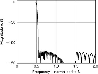
In other applications, such as low frequency, high resolution 24-bit measurement sigma–delta ADCs (such as the AD77xx-series), other types of digital filters may be used. For instance, the SINC3 response is popular because it has zeros at multiples of the throughput rate. For instance a 10 Hz throughput rate produces zeros at 50 Hz and 60 Hz which aid in AC power line rejection. The frequency response of a typical ΣΔ ADC, the AD7730, is shown in Figure 6-103.

High Resolution Measurement Sigma–Delta ADCs
In order to better understand the capability of sigma–delta measurement ADCs and the power of the technique, a modern example, the AD7730, will be examined in detail. The AD7730 is a member of the AD77XX family and is shown in Figure 6-104. This ADC was specifically designed to interface directly to bridge outputs in weigh scale applications. The device accepts low level signals directly from a bridge and outputs a serial digital word. There are two buffered differential inputs which are multiplexed, buffered, and drive a PGA. The PGA can be programmed for four differential unipolar analog input ranges: 0 V to + 10 mV, 0 V to +20 mV, 0 V to +40 mV, and 0 V to +80 mV, and four differential bipolar input ranges: ±10 mV, ±20 mV, ±40 mV, and ±80 mV.

The maximum peak-to-peak, or noise-free resolution achievable is 1 in 230,000 counts, or approximately 18 bits. It should be noted that the noise-free resolution is a function of input voltage range, filter cutoff, and output word rate. Noise is greater using the smaller input ranges where the PGA gain must be increased. Higher output word rates and associated higher filter cutoff frequencies will also increase the noise.
The analog inputs are buffered on-chip allowing relatively high source impedances. Both analog channels are differential, with a CMV range that comes within 1.2 V of analog ground (AGND) and 0.95 V of AVDD. The reference input is also differential, and the common-mode range is from AGND to AVDD.
The 6-bit DAC is controlled by on-chip registers and can remove TARE (pan weight) values of up to ±80 mV from the analog input signal range. The resolution of the TARE function is 1.25 mV with a +2.5 V reference and 2.5 mV with a +5 V reference.
The output of the PGA is applied to the Σ–Δ modulator and programmable digital filter. The serial interface can be configured for three-wire operation and is compatible with microcontrollers and DSPs. The AD7730 contains self-calibration and system-calibration options and has an offset drift of less than 5 nV/°C and a gain drift of less than 2 ppm/°C. This low offset drift is obtained using a chop mode which operates similarly to a chopper-stabilized amplifier.
The oversampling frequency of the AD7730 is 4.9152 MHz, and the output data rate can be set from 50 Hz to 1,200 Hz. The accuracy of the output of the ADC is dependent on the output data rate as shown in Tables I and II of Figure 6-105. These are taken from the AD7730. Note that the accuracy is also dependent on the PGA gain as well.
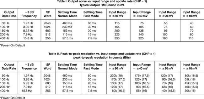
This is easy to understand. The quantization is performed at the master clock rate (4.9152 MHz). If the data rate is increased, there is less time for filtering, so the measured result is noisier. Also as gain is increased, noise is increased as well.
While the output data word is 24-bits wide, there will not be a constant 24-bit data output, even with the input grounded. As seen in Table I, the maximum accuracy is on the order of 18 bits peak-to-peak. This gives rise to a new way of specifying accuracy. This is noise-free counts. For the AD7730 this is 230,000.
The clock source can be provided via an external clock or by connecting a crystal oscillator across the MCLK IN and MCLK OUT pins.
The AD7730 can accept input signals from a DC-excited bridge. It can also handle input signals from an
AC-excited bridge by using the AC excitation clock signals (ACX and ![]() ). These are non-overlapping clock signals used to synchronize the external switches which drive the bridge. The ACX clocks are demodulated on the AD7730 input.
). These are non-overlapping clock signals used to synchronize the external switches which drive the bridge. The ACX clocks are demodulated on the AD7730 input.
The AD7730 contains two 100 nA constant current generators, one source current from AVDD to AIN(+) and one sink current from AIN(−) to AGND. The currents are switched to the selected analog input pair under the control of a bit in the mode register. These currents can be used in checking that a sensor is still operational before attempting to take measurements on that channel. If the currents are turned on and a full-scale reading is obtained, then the sensor has gone open circuit. If the measurement is 0 V, the sensor has gone short circuit. In normal operation, the burnout currents are turned off by setting the proper bit in the mode register to 0.
The AD7730 contains an internal programmable digital filter. The filter consists of two sections: a first stage filter, and a second stage filter. The first stage is a sinc3 LPF. The cutoff frequency and output rate of this first stage filter is programmable. The second stage filter has three modes of operation. In its normal mode, it is a 22-tap FIR filter that processes the output of the first stage filter. When a step change is detected on the analog input, the second stage filter enters a second mode (FASTStep™) where it performs a variable number of averages for some time after the step change, and then the second stage filter switches back to the FIR filter mode. The third option for the second stage filter (SKIP mode) is that it is completely bypassed so the only filtering provided on the AD7730 is the first stage. Both the FASTStep mode and SKIP mode can be enabled or disabled via bits in the control register. Again, there will be an affect on accuracy.
Figure 6-106 shows the full frequency response of the AD7730 when the second stage filter is set for normal FIR operation. This response is with the chop mode enabled and an output word rate of 200 Hz and a clock frequency of 4.9152 MHz. The response is shown from DC to 100 Hz. The rejection at 50 Hz ±1 Hz and 60 Hz ± 1 Hz is better than 88 dB.

Figure 6-107 shows the step response of the AD7730 with and without the FASTStep mode enabled. The vertical axis shows the code value and indicates the settling of the output to the input step change. The horizontal axis shows the number of output words required for that settling to occur. The positive input step change occurs at the 5th output.

In the normal mode (FASTStep disabled), the output has not reached its final value until the 23rd output word. In FASTStep mode with chopping enabled, the output has settled to the final value by the 7th output word. Between the 7th and the 23rd output, the FASTStep mode produces a settled result, but with additional noise compared to the specified noise level for normal operating conditions. It starts at a noise level comparable to the SKIP mode, and as the averaging increases ends up at the specified noise level. The complete settling time required for the part to return to the specified noise level is the same for FASTStep mode and normal mode. The FASTStep mode gives a much earlier indication of where the output channel is going and its new value. This feature is very useful in weigh scale applications to give a much earlier indication of the weight, or in an application scanning multiple channels where the user does not have to wait the full settling time to see if a channel has changed.
Note, however, that the FASTStep mode is not particularly suitable for multiplexed applications because of the excess noise associated with the settling time. For multiplexed applications, the full 23-cycle output word interval should be allowed for settling to a new channel. This points out the fundamental issue of using Σ–Δ ADCs in multiplexed applications. There is no reason why they won’t work, provided the internal digital filter is allowed to settle fully after switching channels.
The AD7730 gives the user access to the on-chip calibration registers allowing an external microprocessor to read the device’s calibration coefficients and also to write its own calibration coefficients to the part from prestored values in external E2PROM. This gives the microprocessor much greater control over the AD7730’s calibration procedure. It also means that the user can verify that the device has performed its calibration correctly by comparing the coefficients after calibration with prestored values in E2PROM. Since the calibration coefficients are derived by performing a conversion on the input voltage provided, the accuracy of the calibration can only be as good as the noise level the part provides in the normal mode. To optimize calibration accuracy, it is recommended to calibrate the part at its lowest output rate where the noise level is lowest. The coefficients generated at any output rate will be valid for all selected output update rates. This scheme of calibrating at the lowest output data rate does mean that the duration of the calibration interval is longer.
The AD7730 requires an external voltage reference, however, the power supply may be used as the reference in the ratiometric bridge application shown in Figure 6-108. In this configuration, the bridge output voltage is directly proportional to the bridge drive voltage which is also used to establish the reference voltages to the AD7730. Variations in the supply voltage will not affect the accuracy. The SENSE outputs of the bridge are used for the AD7730 reference voltages in order to eliminate errors caused by voltage drops in the lead resistances.

Bandpass Sigma–Delta Converters
The Σ–Δ ADCs that we have described so far contain integrators, which are LPFs, whose passband extends from DC. Thus, their quantization noise is pushed up in frequency. At present, most commercially available Σ–Δ ADCs are of this type (although some which are intended for use in audio or telecommunications applications contains bandpass rather than lowpass digital filters to eliminate any system DC offsets). But there is no particular reason why the filters of the Σ–Δ modulator should be LPFs, except that traditionally ADCs have been thought of as being baseband devices, and that integrators are somewhat easier to construct than bandpass filters (BPFs). If we replace the integrators in a Σ–Δ ADC with BPFs as shown in Figure 6-109, the quantization noise is moved up and down in frequency to leave a virtually noise-free region in the passband (see References 31–33). If the digital filter is then programmed to have its passband in this region, we have a Σ–Δ ADC with a bandpass, rather than a lowpass characteristic. Such devices would appear to be useful in direct IF-to-digital conversion, digital radios, ultrasound, and other undersampling applications. However, the modulator and the digital BPF must be designed for the specific set of frequencies required by the system application, thereby somewhat limiting the flexibility of this approach.

In an undersampling application of a bandpass Σ–Δ ADC, the minimum sampling frequency must be at least twice the signal bandwidth, BW. The signal is centered around a carrier frequency, fc. A typical digital radio application using a 455 kHz center frequency and a signal bandwidth of 10 kHz is described in Reference 102. An oversampling frequency KfS = 2 MSPS and an output rate fS = 20 kSPS yielded a dynamic range of 70 dB within the signal bandwidth.
Another example of a bandpass is the AD9870 IF Digitizing Subsystem having a nominal oversampling frequency of 18 MSPS, a center frequency of 2.25 MHz, and a bandwidth of 10–150 kHz (see details in Reference 32).
Sigma–Delta DACs
Sigma–delta DACs operate very similarly to sigma–delta ADCs, however in a sigma–delta DAC, the noise shaping function is accomplished with a digital modulator rather than an analog one.
A Σ–Δ DAC, unlike the Σ–Δ ADC, is mostly digital (see Figure 6-110(A)). It consists of an “interpolation filter” (a digital circuit which accepts data at a low rate, inserts zeros at a high rate, and then applies a digital filter algorithm and outputs data at a high rate), a Σ–Δ modulator (which effectively acts as an LPF to the signal but as a highpass filter to the quantization noise, and converts the resulting data to a high speed bit stream), and a 1-bit DAC whose output switches between equal positive and negative reference voltages. The output is filtered in an external analog LPF. Because of the high oversampling frequency, the complexity of the LPF is much less than the case of traditional Nyquist operation.
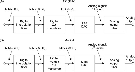
It is possible to use more than 1 bit in the Σ–Δ DAC, and this leads to the multibit architecture shown in Figure 6-110B. The concept is similar to that of interpolating DACs previously discussed in this Chapter, with the addition of the digital sigma–delta modulator. In the past, multibit DACs have been difficult to design because of the accuracy requirement on the n-bit internal DAC (this DAC, although only n-bits, must have the linearity of the final number of bits, N). The AD185x-series of audio DACs, however, use a proprietary data scrambling technique (called data directed scrambling) which overcomes this problem and produces excellent performance with respect to all audio specifications (see References 27 and 28). For instance, the AD1853 dual 24-bit, 92-kSPS DAC has greater than 104 dB total harmonic distortion plus noise (THD + N) at a 48-kSPS sampling rate.
One of the newest members of this family is the AD1955 multibit sigma–delta audio DAC shown in Figure 6-111. The AD1955 also uses data directed scrambling, supports a multitude of DVD audio formats and has an extremely flexible serial port. THD + N is typically 110 dB.
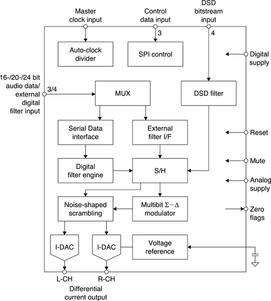
Summary
Sigma–delta ADCs and DACs have proliferated into many modern applications including measurement, voiceband, audio, etc. The technique takes full advantage of low cost CMOS processes and therefore makes integration with highly digital functions such as DSPs practical. Resolutions up to 24-bits are currently available, and the requirements on analog antialiasing/antiimaging filters are greatly relaxed due to oversampling. Modern techniques such as the multibit data scrambled architecture minimize problems with idle tones which plagued early sigma–delta products.
Many sigma–delta converters offer a high level of user programmability with respect to output data rate, digital filter characteristics, and self-calibration modes. Multi-channel sigma–delta ADCs are now available for data acquisition systems, and most users are well-educated with respect to the settling time requirements of the internal digital filter in these applications.
References: Sigma–Delta Converters
1 Hauser M.W. Principles of Oversampling A/D Conversion. Journal Audio Engineering Society. 1991;Vol. 39(1/2):3–26. January/December, (One of the best tutorials and practical discussions of the sigma-delta ADC architecture and its history.)
2 E.M. Deloraine, S. Van Mierlo, and B. Derjavitch, “Methode et systéme de transmission par impulsions,” French Patent 932,140, issued August, 1946. Also British Patent 627,262, issued 1949.
3 E.M. Deloraine, S. Van Mierlo, and B. Derjavitch, “Communication System Utilizing Constant Amplitude Pulses of Opposite Polarities,” US Patent 2,629,857, filed, October 8, 1947, issued February 24, 1953.
4 de Jager F. Delta Modulation: A Method of PCM Transmission Using the One Unit Code. Phillips Research Reports. 1952;Vol. 7:542–546. (Additional work done on delta modulation during the same time period.)
5 Van de Weg H. Quantizing Noise of a Single Integration Delta Modulation System with an N-Digit Code. Phillips Research Reports. 1953;Vol. 8:367–385. (Additional work done on delta modulation during the same time period.)
6 C.C. Cutler, “Differential Quantization of Communication Signals,” US Patent 2,605,361, filed, June 29, 1950, issued July 29, 1952. (Recognized as the first patent on differential PCM or delta modulation, although actually first invented in the Paris labs of the International Telephone and Telegraph Corporation by E. M. Deloraine, S. Mierlo and B. Derjavitch a few years earlier.)
7 C.C. Cutler, “Transmission Systems Employing Quantization,” US Patent 2,927,962, filed, April 26, 1954, issued March 8, 1960. (A. ground-breaking patent describing oversampling and noise shaping. using first and second-order loops to increase effective resolution. The goal was transmission of oversampled noise shaped PCM data without decimation, not a Nyquist-type ADC.)
8 C.B. Brahm, “Feedback Integrating System,” US Patent 3,192,371, filed, September 14, 1961, issued June 29, 1965. (Describes a second-order multibit oversampling noise shaping ADC.)
9 Inose H., Yasuda Y., Murakami J. A Telemetering System by Code Modulation: Δ – Σ Modulation. IRE Transactions on Space Electronics Telemetry. 1962;Vol. SET-8:204–209. September Reprinted in N. S. Jayant, Waveform Quantization and Coding, IEEE Press and John Wiley, 1976, ISBN 0-471-01970-4. (An elaboration on the 1-bit form of Cutler’s noise-shaping oversampling concept. This work coined the description of the architecture as “delta-sigma modulation.”)
10 Inose H., Yasuda Y. A Unity Bit Coding Method by Negative Feedback. IEEE Proceedings. 1963;Vol. 51:1524–1535. November (Further discussions on their 1-bit “delta-sigma” concept.)
11 Goodman D.J.. The Application of Delta Modulation of Analog-to-PCM Encoding. Bell System Technical Journal. 1969;Vol. 48:321–343. February Reprinted in N. S. Jayant, Waveform Quantization and Coding, IEEE Press and John Wiley, 1976, ISBN 0-471-01970-4. (The first description of using oversampling and noise shaping techniques followed by digital filtering and decimation to produce a true Nyquist-rate ADC.).
12 Candy J.C. A Use of Limit Cycle Oscillations to Obtain Robust Analog-to-Digital Converters. IEEE Transactions on Communications. 1974;Vol. COM-22:298–305. December (Describes a multibit oversampling noise shaping ADC with output digital filtering and decimation to interpolate between the quantization levels.)
13 van de Plassche R.J. A Sigma-Delta Modulator as an A/D Converter. IEEE Transactions on Circuits and Systems. 1978;Vol. CAS-25:510–514. July
14 Wooley B.A., Henry J.L. An Integrated Per-Channel PCM Encoder Based on Interpolation. IEEE Journal of Solid State Circuits. 1979;Vol. SC-14:14–20. February (One of the first all-integrated CMOS sigma-delta ADCs.)
15 Wooley B.A., et al. An Integrated Interpolative PCM Decoder. IEEE Journal of Solid State Circuits. 1979;Vol. SC-14:20–25. February
16 Candy J.C., Wooley B.A., Benjamin O.J. A Voiceband Codec with Digital Filtering. IEEE Transactions on Communications. 1981;Vol. COM-29:815–830. June
17 Candy J.C., Temes G.C. Oversampling Delta-Sigma Data Converters. Piscataway, NJ: IEEE Press, 1992. ISBN 0-87942-258-8.
18 Koch R., Heise B., Eckbauer F., Engelhardt E., Fisher J., Parzefall F. A 12-bit Sigma-Delta Analog-to-Digital Converter with a 15 MHz Clock Rate. IEEE Journal of Solid-State Circuits. Vol. SC-21(6), 1986. December.
19 Welland D.R., Del Signore B.P., Swanson E.J. A Stereo 16-Bit Delta-Sigma A/D Converter for Digital Audio. Journal of Audio Engineering Society. 1989;Vol. 37(6):476–485. June
20 Boser B., Wooley B. The Design of Sigma-Delta Modulation Analog-to-Digital Converters. IEEE Journal of Solid-State Circuits. 1988;Vol. 23(6):1298–1308. December
21 J. Dattorro, A. Charpentier, D. Andreas, The Implementation of a One-Stage Multirate 64:1 FIR Decimator for use in One-Bit Sigma-Delta A/D Applications. AES 7th International Conference, May, 1989.
22 W.L. Lee and C.G. Sodini, “A Topology for Higher-Order Interpolative Coders,” ISCAS PROC., 1987.
23 Ferguson P.F., Jr., Ganesan A., Adams R.W. One-Bit Higher Order Sigma-Delta A/D Converters. ISCAS PROC. 1990;Vol. 2:890–893.
24 W.L. Lee, A Novel Higher Order Interpolative Modulator Topology for High Resolution Oversampling A/D Converters, MIT Masters Thesis, June, 1987.
25 Adams R.W. Design and Implementation of an Audio 18-Bit Analog-to-Digital Converter Using Oversampling Techniques. Journal of Audio Engineering Society. 1986;Vol. 34:153–166. March
26 P. Ferguson, Jr., A. Ganesan, R. Adams, et. al., “An 18-Bit 20-kHz Dual Sigma-Delta A/D Converter,” ISSCC Digest of Technical Papers, February, 1991.
27 Adams R., Nguyen K., Sweetland K. A 113 dB SNR Oversampling DAC with Segmented Noise-Shaped Scrambling. ISSCC Digest of Technical Papers. 1998;Vol. 41:62. 63, 413. (Describes a segmented audio DAC with data scrambling.)
28 R.W. Adams and T.W. Kwan, “Data-directed Scrambler for Multi-bit Noise-shaping D/A Converters,” US Patent 5,404,142, filed, August 5, 1993, issued April 4, 1995. (Describes a segmented audio DAC with data scrambling.)
29 Matsuya Y., et al. A 16-Bit Oversampling A/D Conversion Technology Using Triple-Integration Noise Shaping. IEEE Journal of Solid-State Circuits. 1987;Vol. SC-22(6):921–929. December
30 Matsuya Y., et al. A 17-Bit Oversampling D/A Conversion Technology Using Multistage Noise Shaping. IEEE Journal of Solid-State Circuits. 1989;Vol. 24(4):969–975. August
31 P.H. Gailus, W.J. Turney, and F.R. Yester, Jr., “Method and Arrangement for a Sigma-Delta Converter for Bandpass Signals,” US Patent 4,857,928, filed, January 28, 1988, issued August 15, 1989.
32 Jantzi S.A., Snelgrove M., Ferguson P.F., Jr. A 4th-Order Bandpass Sigma-Delta Modulator. IEEE Journal of Solid State Circuits. 1993;Vol. 38(3):282–291. March
33 Hendriks P., Schreier R., DiPilato J.. High Performance Narrowband Receiver Design Simplified by IF Digitizing Subsystem in LQFP. Analog Dialogue. 2001;Vol. 35(3). June-July, available at http://www.analog.com (describes an IF subsystem with a bandpass sigma-delta ADC having a nominal oversampling frequency of 18 MSPS, a center frequency of 2.25 MHz, and a bandwidth of 10 kHz-150 kHz)..