CHAPTER 5 Fundamentals of Sampled Data Systems
SECTION 5-1 Coding and Quantizing
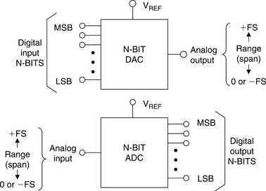
Analog-to-digital converters (ADCs) translate analog measurements, which are characteristic of most phenomena in the “real world,” to digital language, used in information processing, computing, data transmission, and control systems. Digital-to-analog converters (DACs) are used in transforming transmitted or stored data, or the results of digital processing, back to “real-world” variables for control, information display, or further analog processing. The relationships between inputs and outputs of ADCs and DACs are shown in Figure 5-1.
Analog input variables, whatever their origin, are most frequently converted by transducers into voltages or currents. These electrical quantities may appear as fast or slow “DC” continuous direct measurements of a phenomenon in the time domain, as modulated AC waveforms (using a wide variety of modulation techniques), or in some combination, with a spatial configuration of related variables to represent shaft angles. Examples of the first are outputs of thermocouples, potentiometers on DC references, and analog computing circuitry; of the second, “chopped” optical measurements, AC strain gauge or bridge outputs, and digital signals buried in noise; and of the third, synchros and resolvers.
The analog variables to be dealt with in this chapter are those involving voltages or currents representing the actual analog phenomena. They may be either wideband or narrowband. They may be either scaled from the direct measurement or subjected to some form of analog pre-processing, such as linearization, combination, demodulation, filtering, sample–hold, etc.
As part of the process, the voltages and currents are “normalized” to ranges compatible with assigned ADC input ranges. Analog output voltages or currents from DACs are direct and in normalized form, but they may be subsequently post-processed (e.g., scaled, filtered, amplified, etc.).
Information in digital form is normally represented by arbitrarily fixed voltage levels referred to “ground,” either occurring at the outputs of logic gates or applied to their inputs. The digital numbers used are all basically binary; i.e., each “bit,” or unit of information, has one of two possible states. These states are “off,” “false,” or “0,” and “on,” “true,” or “1.” It is also possible to represent the two logic states by two different levels of current; however, this is much less popular than using voltages. There is also no particular reason why the voltages need be referenced to ground—as in the case of emitter-coupled logic (ECL), positive-emitter-coupled logic (PECL), or low-voltage-differential-signaling logic (LVDS), for example.
Words are groups of levels representing digital numbers; the levels may appear simultaneously in parallel, on a bus or groups of gate inputs or outputs, serially (or in a time sequence) on a single line, or as a sequence of parallel bytes (i.e., “byte-serial”) or nibbles (small bytes). For example, a 16-bit word may occupy the 16 bits of a 16-bit bus, or it may be divided into two sequential bytes for an 8-bit bus, or four 4-bit nibbles for a 4-bit bus.
A unique parallel or serial grouping of digital levels, or a number, or code, is assigned to each analog level which is quantized (i.e., represents a unique portion of the analog range). A typical digital code would be this array:
It is composed of 8 bits. The “1” at the extreme left is called the “most significant bit” (MSB, or Bit 1), and the one at the right is called the “least significant bit” (LSB, or Bit N: 8 in this case). The meaning of the code, as either a number, a character, or a representation of an analog variable, is unknown until the code and the conversion relationship have been defined. It is important not to confuse the designation of a particular bit (i.e., Bit 1, Bit 2, etc.) with the subscripts associated with the “a” array. The subscripts correspond to power of 2 associated with the weight of a particular bit in the sequence.
The best-known code is natural or straight binary (base 2). Binary codes are most familiar in representing integers; i.e., in a natural binary integer code having N bits, the LSB has a weight of 20 (i.e., 1), the next bit has a weight of 21 (i.e., 2), and so on up to the MSB, which has a weight of 2N–1 (i.e., 2N/2). The value of a binary number is obtained by adding up the weights of all non-zero bits. When the weighted bits are added up, they form a unique number having any value from 0 to 2N–1.
Often, for convenience, a binary number is expressing in hexadecimal (base 16). This reduces the length of the word and makes it easier to read. Figure 5-2 shows the relationship between binary and hexadecimal (commonly referred to as “hex”).
In converter technology, full-scale (abbreviated FS) is independent of the number of bits of resolution, N. A more useful coding is fractional binary which is always normalized to full-scale. Integer binary can be interpreted as fractional binary if all integer values are divided by 2N. For example, the MSB has a weight of 1/2 (i.e., 2(N–1)/2N = 21), the next bit has a weight of 1/4 (i.e., 2−2), and so forth down to the LSB, which has a weight of 1/2N (i.e., 2−N). When the weighted bits are added up, they form a number with any of 2N values, from 0 to (1-2−N) of full-scale. Additional bits simply provide more fine structure without affecting full-scale range. The relationship between base 10 numbers and binary numbers (base 2) are shown in Figure 5-3 along with examples of each.
Unipolar Codes
In data conversion systems, the coding method must be related to the analog input range (or span) of an ADC or the analog output range (or span) of a DAC. The simplest case is when the input to the ADC or the output of the DAC is always a unipolar positive voltage (current outputs are very popular for DAC outputs, much less for ADC inputs). The most popular code for this type of signal is straight binary and is shown in Figure 5-4 for a 4-bit converter. Notice that there are 16 distinct possible levels, ranging from the all-zeros code 0000, to the all-ones code 1111. It is important to note that the analog value represented by the all-ones code is not full-scale (abbreviated FS), but FS −1 LSB. This is a common convention in data conversion notation and applies to both ADCs and DACs. Figure 5-4 gives the base 10 equivalent number, the value of the base 2 binary code relative to full-scale (FS), and also the corresponding voltage level for each code (assuming a + 10 V full-scale converter).
Figure 5-5 shows the transfer function for an ideal 3-bit DAC with straight binary input coding. Notice that the analog output is zero for the all-zeros input code. As the digital input code increases, the analog output increases 1 LSB (1/8 scale in this example) per code. The most positive output voltage is 7/8 FS, corresponding to a value equal to FS −1 LSB. The mid-scale output of 1/2 FS is generated when the digital input code is 100.
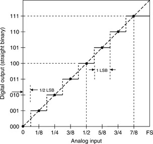
The transfer function of an ideal 3-bit ADC is shown in Figure 5-6. There is a range of analog input voltage over which the ADC will produce a given output code, and this range is the quantization uncertainty and is equal to 1 LSB. Note that the width of the transition regions between adjacent codes is zero for an ideal ADC. In practice, however, there is always transition noise associated with these levels, and therefore the width is non-zero. It is customary to define the analog input corresponding to a given code by the code center which lies halfway between two adjacent transition regions (illustrated by the black dots in the diagram). This requires that the first transition region occur at 1/2 LSB. The full-scale analog input voltage is defined by 7/8 FS (FS −1 LSB).
Bipolar Codes
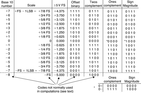
In many systems, it is desirable to represent both positive and negative analog quantities with binary codes. Either offset binary, twos complement, ones complement, or sign-magnitude codes will accomplish this, but offset binary and twos complement are by far the most popular. The relationships between these codes for a 4-bit system are shown in Figure 5-7. Note that the values are scaled for a ± 5 V full-scale input/output voltage range.
For offset binary, the zero signal value is assigned the code 1000. The sequence of codes is identical to that of straight binary. The only difference between a straight and offset binary system is the half-scale offset associated with analog signal. The most negative value (–FS + 1 LSB) is assigned the code 0001, and the most positive value (+FS −1 LSB) is assigned the code 1111. Note that in order to maintain perfect symmetry about mid-scale, the all-zeros code (0000) representing negative full-scale (–FS) is not normally used in computation. It can be used to represent a negative off-range condition or simply assigned the value of the 0001 (–FS + 1 LSB).
The relationship between the offset binary code and the analog output range of a bipolar 3-bit DAC is shown in Figure 5-8. The analog output of the DAC is zero for the zero-value input code 100. The most negative output voltage is generally defined by the 001 code (–FS + 1 LSB), and the most positive by 111 (+FS −1 LSB). The output voltage for the 000 input code is available for use if desired but makes the output non-symmetrical about zero and complicates the mathematics.
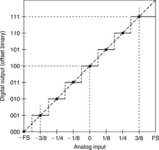
The offset binary output code a bipolar 3-bit ADC as a function of its analog input is shown in Figure 5-9. Note that zero analog input defines the center of the mid-scale code 100. As in the case of bipolar DACs, the most negative input voltage is generally defined by the 001 code (–FS + 1 LSB), and the most positive by 111 (+FS −1 LSB). As discussed above, the 000 output code is available for use if desired but makes the output non-symmetrical about zero and complicates the mathematics.
Twos complement is identical to offset binary with the MSB complemented (inverted). This is obviously very easy to accomplish in a data converter, using a simple inverter or taking the complementary output of a “D” flip-flop. The popularity of twos complement coding lies in the ease with which mathematical operations can be performed in computers. Twos complement, for conversion purposes, consists of a binary code for positive magnitudes (0 sign bit), and the twos complement of each positive number to represent its negative. The twos complement is formed arithmetically by complementing the number and adding 1 LSB. For example, −3/8 FS is obtained by taking the twos complement of +3/8 FS. This is done by first complementing +3/8 FS, 0011 obtaining 1100. Adding 1 LSB, we obtain 1101.
Twos complement makes subtraction easy. For example, to subtract 3/8 FS from 4/8 FS, add 4/8 to −3/8, or 0100 to 1101. The result is 0001, disregarding the extra carry, or 1/8.
Ones complement can also be used to represent negative numbers, although it is much less popular than twos complement and rarely used today. The ones complement is obtained by simply complementing all of a positive numbers digits. For instance, the ones complement of 3/8 FS (0011) is 1100. A ones complemented code can be formed by complementing each positive value to obtain its corresponding negative value. This includes zero, which is then represented by either of two codes, 0000 (referred to as 0+) and 1111 (referred to as 0–). This ambiguity must be dealt with mathematically, and presents obvious problems relating to ADCs and DACs for which there is a single code which represents zero.
Sign magnitude would appear to be the most straightforward way of expressing signed analog quantities digitally. Simply determine the code appropriate for the magnitude and add a polarity bit. Sign-magnitude binary-coded decimal (BCD) is popular in bipolar digital voltmeters (DVMs), but has the problem of two allowable codes for zero. It is therefore unpopular for most applications involving ADCs or DACs.
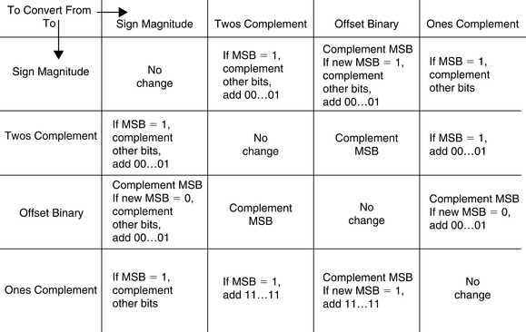
Figure 5-10 summarizes the relationships between the various bipolar codes: offset binary, twos complement, ones complement, and sign magnitude and shows how to convert between them.
The last code to be considered in this section is BCD, where each base 10 digit (0 to 9) in a decimal number is represented as the corresponding 4-bit straight binary word as shown in Figure 5-11. The minimum digit 0 is represented as 0000, and the digit 9 by 1001. This code is relatively inefficient, since only 10 of the 16 code states for each decade are used. It is, however, a very useful code for interfacing to decimal displays such as in DVMs.
Complementary Codes
Some forms of data converters (e.g., early DACs using monolithic NPN quad current switches) require standard codes such as natural binary or BCD, but with all bits represented by their complements. Such codes are called complementary codes. All the codes discussed thus far have complementary codes which can be obtained by this method.
In a 4-bit complementary-binary converter, 0 is represented by 1111, half-scale by 0111, and FS −1 LSB by 0000. In practice, the complementary code can usually be obtained by using the complementary output of a register rather than the true output, since both are available.
Sometimes the complementary code is useful in inverting the analog output of a DAC. Today many DACs provide differential outputs which allow the polarity inversion to be accomplished without modifying the input code. Similarly, many ADCs provide differential logic inputs which can be used to accomplish the polarity inversion.
DAC and ADC Static Transfer Functions and DC Errors
The most important thing to remember about both DACs and ADCs is that either the input or output is digital, and therefore the signal is quantized. That is, an N-bit word represents one of 2N possible states, and therefore an N-bit DAC (with a fixed reference) can have only 2N possible analog outputs, and an N-bit ADC can have only 2N possible digital outputs. As previously discussed, the analog signals will generally be voltages or currents.
The resolution of data converters may be expressed in several different ways: the weight of the least significant bit (LSB), parts per million of full-scale (ppm FS), millivolts (mV), etc. Different devices (even from the same manufacturer) will be specified differently, so converter users must learn to translate between the different types of specifications if they are to compare devices successfully. The size of the LSB for various resolutions is shown in Figure 5-12.
Before we can consider the various architectures used in data converters, it is necessary to consider the performance to be expected, and the specifications which are important. The following sections will consider the definition of errors and specifications used for data converters. This is important in understanding the strengths and weaknesses of different ADC/DAC architectures.
Figure 5-13 shows the ideal transfer characteristics for a 3-bit unipolar DAC and a 3-bit unipolar ADC. In a DAC, both the input and the output are quantized, and the graph consists of eight points—while it is reasonable to discuss the line through these points, it is very important to remember that the actual transfer characteristic is not a line, but a number of discrete points.
The input to an ADC is analog and is not quantized, but its output is quantized. The transfer characteristic therefore consists of eight horizontal steps. When considering the offset, gain, and linearity of an ADC we consider the line joining the midpoints of these steps—often referred to as the code centers.
For both DACs and ADCs, digital full-scale (all “1”s) corresponds to 1 LSB below the analog full-scale (FS). The (ideal) ADC transitions take place at 1/2 LSB above zero, and thereafter every LSB, until 1 1/2 LSB below analog full-scale. Since the analog input to an ADC can take any value, but the digital output is quantized, there may be a difference of up to 1/2 LSB between the actual analog input and the exact value of the digital output. This is known as the quantization error or quantization uncertainty as shown in Figure 5-15. In AC (sampling) applications this quantization error gives rise to quantization noise which will be discussed in Section 5-2 of this chapter.
As previously discussed, there are many possible digital coding schemes for data converters: straight binary, offset binary, ones complement, twos complement, sign-magnitude, gray code, BCD, and others. This section, being devoted mainly to the analog issues surrounding data converters, will use simple binary and offset binary in its examples and will not consider the merits and disadvantages of these, or any other forms of digital code.
The examples in Figure 5-13 use unipolar converters, whose analog port has only a single polarity. These are the simplest type, but bipolar converters are generally more useful in real-world applications.
There are two types of bipolar converters: the simpler is merely a unipolar converter with an accurate 1 MSB of negative offset (and many converters are arranged so that this offset may be switched in and out so that they can be used as either unipolar or bipolar converters at will), but the other, known as a sign-magnitude converter, is more complex, and has N bits of magnitude information and an additional bit which corresponds to the sign of the analog signal. Sign-magnitude DACs are quite rare, and sign-magnitude ADCs are found mostly in DVMs. The unipolar, offset binary, and sign-magnitude representations are shown in Figure 5-14.
The four DC errors in a data converter are offset error, gain error, and two types of linearity error (differential and integral). Offset and gain errors are analogous to offset and gain errors in amplifiers as shown in Figure 5-15 for a bipolar input range (though offset error and zero error, which are identical in amplifiers and unipolar data converters, are not identical in bipolar converters and should be carefully distinguished). The transfer characteristics of both DACs and ADCs may be expressed as D = K + GA, where D is the digital code, A is the analog signal, and K and G are constants. In a unipolar converter, K is zero, and in an offset bipolar converter, it is −1 MSB. The offset error is the amount by which the actual value of K differs from its ideal value.
The gain error is the amount by which G differs from its ideal value, and is generally expressed as the percentage difference between the two, although it may be defined as the gain error contribution (in mV or LSB) to the total error at full-scale. These errors can usually be trimmed by the data converter user. Note, however, that amplifier offset is trimmed at zero input, and then the gain is trimmed near to full-scale. The trim algorithm for a bipolar data converter is not so straightforward.
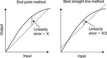
The integral linearity error of a converter is also analogous to the linearity error of an amplifier, is defined as the maximum deviation of the actual transfer characteristic of the converter from a straight line, and is generally expressed as a percentage of full-scale (but may be given in LSBs). For an ADC, the most popular convention is to draw the straight line through the midpoints of the codes, or the code centers. There are two common ways of choosing the straight line: end point and best straight line as shown in Figure 5-16.
In the end point system, the deviation is measured from the straight line through the origin and the full-scale point (after gain adjustment). This is the most useful integral linearity measurement for measurement and control applications of data converters (since error budgets depend on deviation from the ideal transfer characteristic, not from some arbitrary “best fit”), and is the one normally adopted by Analog Devices, Inc.
The best straight line, however, does give a better prediction of distortion in AC applications, and also gives a lower value of “linearity error” on a data sheet. The best fit straight line is drawn through the transfer characteristic of the device using standard curve fitting techniques, and the maximum deviation is measured from this line. In general, the integral linearity error measured in this way is only 50% of the value measured by end point methods. This makes the method good for producing impressive data sheets, but it is less useful for error budget analysis. For AC applications, it is even better to specify distortion than DC linearity, so it is rarely necessary to use the best straight line method to define converter linearity.
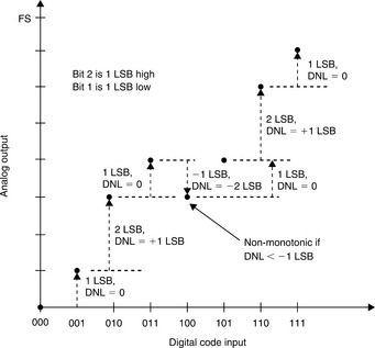
The other type of converter nonlinearity is differential nonlinearity (DNL). This relates to the linearity of the code transitions of the converter. In the ideal case, a change of 1 LSB in digital code corresponds to a change of exactly 1 LSB of analog signal. In a DAC, a change of 1 LSB in digital code produces exactly 1 LSB change of analog output, while in an ADC there should be exactly 1 LSB change of analog input to move from one digital transition to the next. Differential linearity error is defined as the maximum amount of deviation of any quantum (or LSB change) in the entire transfer function from its ideal size of 1 LSB.
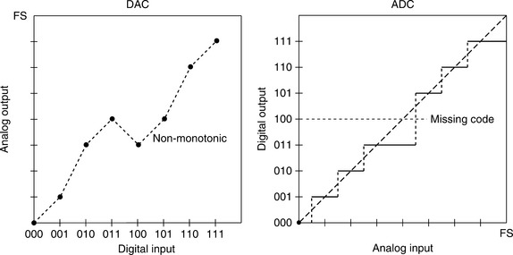
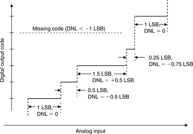
Where the change in analog signal corresponding to 1 LSB digital change is more or less than 1 LSB, there is said to be a DNL error. The DNL error of a converter is normally defined as the maximum value of DNL to be found at any transition across the range of the converter. Figure 5-17 shows the non-ideal transfer functions for a DAC and an ADC and shows the effects of the DNL error.
The DNL of a DAC is examined more closely in Figure 5-18. If the DNL of a DAC is less than −1 LSB at any transition, the DAC is non-monotonic, i.e., its transfer characteristic contains one or more localized maxima or minima. A DNL greater than +1 LSB does not cause non-monotonicity, but is still undesirable. In many DAC applications (especially closed-loop systems where non-monotonicity can change negative feedback to positive feedback), it is critically important that DACs are monotonic. DAC monotonicity is often explicitly specified on data sheets, although if the DNL is guaranteed to be less than 1 LSB (i.e., |DNL| ≤ 1 LSB) then the device must be monotonic, even without an explicit guarantee.
In Figure 5-19, the DNL of an ADC is examined more closely on an expanded scale. ADCs can be non-monotonic, but a more common result of excess DNL in ADCs is missing codes. Missing codes in an ADC are as objectionable as non-monotonicity in a DAC. Again, they result from DNL < −1 LSB.
Not only can ADCs have missing codes, they can also be non-monotonic as shown in Figure 5-20. As in the case of DACs, this can present major problems—especially in servo applications.
In a DAC, there can be no missing codes—each digital input word will produce a corresponding analog output. However, DACs can be non-monotonic as previously discussed. In a straight binary DAC, the most likely place a non-monotonic condition can develop is at mid-scale between the two codes: 011 … 11 and 100 … 00. If a non-monotonic condition occurs here, it is generally because the DAC is not properly calibrated or trimmed. A successive approximation ADC with an internal non-monotonic DAC will generally produce missing codes but remain monotonic. However it is possible for an ADC to be non-monotonic—again depending on the particular conversion architecture. Figure 5-20 shows the transfer function of an ADC which is non-monotonic and has a missing code.
ADCs which use the subranging architecture divide the input range into a number of coarse segments, and each coarse segment is further divided into smaller segments—and ultimately the final code is derived. This process is described in more detail in Chapter 6 of this book. An improperly trimmed subranging ADC may exhibit non-monotonicity, wide codes, or missing codes at the subranging points as shown in Figure 5-21(A)–(C), respectively. This type of ADC should be trimmed so that drift due to aging or temperature produces wide codes at the sensitive points rather than non-monotonic or missing codes.
Defining missing codes is more difficult than defining non-monotonicity. All ADCs suffer from some inherent transition noise as shown in Figure 5-22 (think of it as the flicker between adjacent values of the last digit of a DVM). As resolutions and bandwidths become higher, the range of input over which transition noise occurs may approach, or even exceed, 1 LSB. High resolution wideband ADCs generally have internal noise sources which can be reflected to the input as effective input noise summed with the signal. The effect of this noise, especially if combined with a negative DNL error, may be that there are some (or even all) codes where transition noise is present for the whole range of inputs. There are therefore some codes for which there is no input which will guarantee that code as an output, although there may be a range of inputs which will sometimes produce that code.
For low resolution ADCs, it may be reasonable to define no missing codes as a combination of transition noise and DNL which guarantees some level (perhaps 0.2 LSB) of noise-free code for all codes. However, this is impossible to achieve at the very high resolutions achieved by modern sigma–delta ADCs, or even at lower resolutions in wide bandwidth sampling ADCs. In these cases, the manufacturer must define noise levels and resolution in some other way. Which method is used is less important, but the data sheet should contain a clear definition of the method used and the performance to be expected.
The discussion thus far has not dealt with the most important DC specifications associated with data converters. Other less important specifications require only a definition. There are also AC specifications. Converter specifications are covered in Chapter 6.
References: Coding and Quantizing
1 K.W. Cattermole, Principles of Pulse Code Modulation, American Elsevier Publishing Company, Inc., New York, 1969, ISBN: 444-19747-8 (an excellent tutorial and historical discussion of data conversion theory and practice, oriented towards PCM, but covers practically all aspects. This one is a must for anyone serious about data conversion! Try Internet secondhand bookshops such as http://www.abebooks.com for starters).
2 Frank Gray, “Pulse Code Communication,” US Patent 2,632,058, filed, November 13, 1947, issued March 17, 1953 (detailed patent on the Gray code and its application to electron beam coders).
3 Sears R.W. Electron Beam Deflection Tube for Pulse Code Modulation. Bell System Technical Journal. 1948;Vol. 27:44–57. January(describes an electron-beam deflection tube 7-bit, 100 kSPS flash converter for early experimental PCM work).
4 Edson J.O., Henning H.H. Broadband Codecs for an Experimental 224 Mb/s PCM Terminal. Bell System Technical Journal. 1965;Vol. 44:1887–1940. November(summarizes experiments on ADCs based on the electron tube coder as well as a bit-per-stage Gray code 9-bit solid state ADC. The electron beam coder was 9-bits at 12 MSPS, and represented the fastest of its type).
5 Sheingold Dan. Analog-Digital Conversion Handbook, 3rd Ed. In: the defining and classic book on data conversion. Analog Devices and Prentice-Hall; 1986. ISBN: 0-13-032848-0
SECTION 5-2 Sampling Theory
This section discusses the basics of sampling theory. A block diagram of a typical real-time sampled data system is shown in Figure 5-23. Prior to the actual analog-to-digital conversion, the analog signal usually passes through some sort of signal conditioning circuitry which performs such functions as amplification, attenuation, and filtering. The lowpass/bandpass filter is required to remove unwanted signals outside the bandwidth of interest and prevent aliasing.
The system shown in Figure 5-23 is a real-time system, i.e., the signal to the ADC is continuously sampled at a rate equal to fs, and the ADC presents a new sample to the DSP at this rate. In order to maintain realtime operation, the DSP must perform all its required computation within the sampling interval, 1/fs, and present an output sample to the DAC before arrival of the next sample from the ADC. An example of a typical DSP function would be a digital filter.
In the case of FFT analysis, a block of data is first transferred to the DSP memory. The FFT is calculated at the same time a new block of data is transferred into the memory, in order to maintain real-time operation. The DSP must calculate the FFT during the data transfer interval so it will be ready to process the next block of data.
Note that the DAC is required only if the DSP data must be converted back into an analog signal (as would be the case in a voiceband or audio application, for example). There are many applications where the signal remains entirely in digital format after the initial A/D conversion. Similarly, there are applications where the DSP is solely responsible for generating the signal to the DAC, such as in CD player electronics. If a DAC is used, it must be followed by an analog anti-imaging filter to remove the image frequencies. Finally, there are slower speed industrial process control systems where sampling rates are much lower—regardless of the system, the fundamentals of sampling theory still apply.
There are two key concepts involved in the actual analog-to-digital and digital-to-analog conversion process: discrete time sampling and finite amplitude resolution due to quantization. An understanding of these concepts is vital to data converter applications.
The Need for a Sample-and-Hold Amplifier Function
The generalized block diagram of a sampled data system shown in Figure 5-23 assumes some type of AC signal at the input. It should be noted that this does not necessarily have to be so, as in the case of modern DVMs or ADCs optimized for DC measurements, but for this discussion assume that the input signal has some upper frequency limit fa.
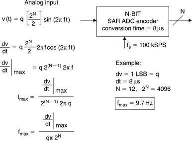
Most ADCs today have a built-in sample-and-hold amplifier (SHA) function, thereby allowing them to process AC signals. This type of ADC is referred to as a sampling ADC. However many early ADCs, such as the Analog Devices’ industry-standard AD574, were not of the sampling type, but simply encoders. If the input signal to a SAR ADC (assuming no SHA function) changes by more than 1 LSB during the conversion time (8 μs in the example), the output data can have large errors, depending on the location of the code as shown in Figure 5-24. Most ADC architectures are subject to this type of error—some more, some less—with the possible exception of very well flash converters having well-matched comparators.
Assume that the input signal to the encoder is a sinewave with a full-scale amplitude (q2N/2), where q is the weight of 1 LSB:
The maximum rate of change is therefore:
If N = 12, and 1 LSB change (dv = q) is allowed during the conversion time (dt = 8 μs), then the equation can be solved for fmax, the maximum full-scale signal frequency that can be processed without error:
This implies any input frequency greater than 9.7 Hz is subject to conversion errors, even though a sampling frequency of 100 kSPS is possible with the 8 μs ADC (this allows an extra 2 μs interval for an external SHA to re-acquire the signal after coming out of the hold mode).
To process AC signals, an SHA function is added. The ideal SHA is simply a switch driving a hold capacitor followed by a high input impedance buffer. The input impedance of the buffer must be high enough so that the capacitor is discharged by less than 1 LSB during the hold time. The SHA samples the signal in the sample mode, and holds the signal constant during the hold mode. The timing is adjusted so that the encoder performs the conversion during the hold time. A sampling ADC can therefore process fast signals—the upper frequency limitation is determined by the SHA aperture jitter, bandwidth, distortion, etc., not the encoder. In the example shown, a good sample-and-hold could acquire the signal in 2 μs, allowing a sampling frequency of 100 kSPS, and the capability of processing input frequencies up to 50 kSPS. A complete discussion of the SHA function including these specifications follows later in this chapter.
The Nyquist Criteria
A continuous analog signal is sampled at discrete intervals, ts = 1/fs, which must be carefully chosen to ensure an accurate representation of the original analog signal. It is clear that the more samples taken (faster sampling rates), the more accurate the digital representation, but if fewer samples are taken (lower sampling rates), a point is reached where critical information about the signal is actually lost. The mathematical basic of sampling was set forth by Harry Nyquist of Bell Telephone Laboratories in two classic papers published in 1924 and 1928, respectively (see References 1 and 2). Nyquist’s original work was shortly supplemented by R.V.L. Hartley (Reference 3). These papers formed the basis for the PCM work to follow in the 1940s, and in 1948 Claude Shannon wrote his classic paper on communication theory (Reference 4).
Simply stated, the Nyquist criteria requires that the sampling frequency be at least twice the highest frequency contained in the signal, or information about the signal will be lost. If the sampling frequency is less than twice the maximum analog signal frequency, a phenomenon known as aliasing will occur (Figure 5-25).
In order to understand the implications of aliasing in both the time and frequency domain, first consider the case of a time domain representation of a single tone sinewave sampled as shown in Figure 5-26. In this example, the sampling frequency fs is not at least 2fa, but only slightly more than the analog input frequency fa—the Nyquist criteria is violated. Notice that the pattern of the actual samples produces an aliased sinewave at a lower frequency equal to fs − fa.
The corresponding frequency domain representation of this scenario is shown in Figure 5-27(B). Now consider the case of a single frequency sinewave of frequency fa sampled at a frequency fs by an ideal impulse sampler (see Figure 5-27(A)). Also assume that fs > 2fa as shown. The frequency domain output of the sampler shows aliases or images of the original signal around every multiple of fs, i.e., at frequencies equal to |±Kfs ± fa|, K=1,2,3,4,….
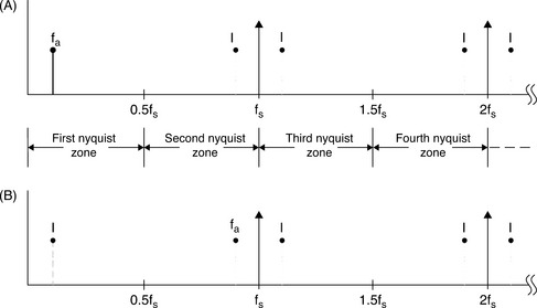
Figure 5-27: Analog signal fa sampled at fs using ideal sampler has images (aliases) at 1 ± Kfs ± fa1, K = 1, 2, 3, …
The Nyquist bandwidth is defined to be the frequency spectrum from DC to fs/2. The frequency spectrum is divided into an infinite number of Nyquist zones, each having a width equal to 0.5fs as shown. In practice, the ideal sampler is replaced by an ADC followed by an FFT processor. The FFT processor only provides an output from DC to fs/2, i.e., the signals or aliases which appear in the first Nyquist zone.
Now consider the case of a signal which is outside the first Nyquist zone (Figure 5-27(B)). The signal frequency is only slightly less than the sampling frequency, corresponding to the condition shown in the time domain representation in Figure 5-26. Notice that even though the signal is outside the first Nyquist zone, its image (or alias), fs − fa, falls inside. Returning to Figure 5-27(A), it is clear that if an unwanted signal appears at any of the image frequencies of fa, it will also occur at fa, thereby producing a spurious frequency component in the first Nyquist zone.
This is similar to the analog mixing process and implies that some filtering ahead of the sampler (or ADC) is required to remove frequency components which are outside the Nyquist bandwidth, but whose aliased components fall inside it. The filter performance will depend on how close the out-of-band signal is to fs/2 and the amount of attenuation required.
Baseband Antialiasing Filters
Baseband sampling implies that the signal to be sampled lies in the first Nyquist zone. It is important to note that with no input filtering at the input of the ideal sampler, any frequency component (either signal or noise) that falls outside the Nyquist bandwidth in any Nyquist zone will be aliased back into the first Nyquist zone. For this reason, an antialiasing filter is used in almost all sampling ADC applications to remove these unwanted signals.
Properly specifying the antialiasing filter is important. The first step is to know the characteristics of the signal being sampled. Assume that the highest frequency of interest is fa. The antialiasing filter passes signals from DC to fa while attenuating signals above fa.
Assume that the corner frequency of the filter is chosen to be equal to fa. The effect of the finite transition from minimum to maximum attenuation on system dynamic range is illustrated in Figure 5-28(A).
Assume that the input signal has full-scale components well above the maximum frequency of interest, fa. The diagram shows how full-scale frequency components above fs − fa are aliased back into the bandwidth DC to fa. These aliased components are indistinguishable from actual signals and therefore limit the dynamic range to the value on the diagram which is shown as DR.
Some texts recommend specifying the antialiasing filter with respect to the Nyquist frequency, fs/2, but this assumes that the signal bandwidth of interest extends from DC to fs/2 which is rarely the case. In the example shown in Figure 5-28, the aliased components between fa and fs/2 are not of interest and do not limit the dynamic range.
The antialiasing filter transition band is therefore determined by the corner frequency fa, the stopband frequency fs − fa, and the desired stopband attenuation, DR. The required system dynamic range is chosen based on the requirement for signal fidelity.
Filters become more complex as the transition band becomes sharper, all other things being equal. For instance, a Butterworth filter gives 6 dB attenuation per octave for each filter pole. Achieving 60 dB attenuation in a transition region between 1 and 2 MHz (1 octave) requires a minimum of 10 poles—not a trivial filter, and definitely a design challenge.
Therefore, other filter types are generally more suited to high speed applications where the requirement is for a sharp transition band and in-band flatness coupled with linear phase response. Elliptic filters meet these criteria and are a popular choice. There are a number of companies which specialize in supplying custom analog filters. TTE is an example of such a company (Reference 5).
From this discussion, we can see how the sharpness of the antialiasing transition band can be traded off against the ADC sampling frequency. Choosing a higher sampling rate (oversampling) reduces the requirement on transition band sharpness (hence, the filter complexity) at the expense of using a faster ADC and processing data at a faster rate. This is illustrated in Figure 5-28(B) which shows the effects of increasing the sampling frequency by a factor of K, while maintaining the same analog corner frequency, fa, and the same dynamic range, DR, requirement. The wider transition band (fa to Kfs − fa) makes this filter easier to design than for the case of Figure 5-28(A).
The antialiasing filter design process is started by choosing an initial sampling rate of 2.5 to 4 times fa. Determine the filter specifications based on the required dynamic range and see if such a filter is realizable within the constraints of the system cost and performance. If not, consider a higher sampling rate which may require using a faster ADC. It should be mentioned that sigma–delta ADCs are inherently oversampling converters, and the resulting relaxation in the analog antialiasing filter requirements is therefore an added benefit of this architecture.
The antialiasing filter requirements can also be relaxed somewhat if it is certain that there will never be a full-scale signal at the stopband frequency fs − fa. In many applications, it is improbable that full-scale signals will occur at this frequency. If the maximum signal at the frequency fs − fa will never exceed X dB below full-scale, then the filter stopband attenuation requirement is reduced by that same amount. The new requirement for stopband attenuation at fs − fa based on this knowledge of the signal is now only DR − X dB. When making this type of assumption, be careful to treat any noise signals which may occur above the maximum signal frequency fa as unwanted signals which will also alias back into the signal bandwidth.
Undersampling
Thus far we have considered the case of baseband sampling, i.e., all the signals of interest lie within the first Nyquist zone. Figure 5-29(A) shows such a case, where the band of sampled signals is limited to the first Nyquist zone, and images of the original band of frequencies appear in each of the other Nyquist zones.
Consider the case shown in Figure 5-29(B), where the sampled signal band lies entirely within the second Nyquist zone. The process of sampling a signal outside the first Nyquist zone is often referred to as undersampling, or harmonic sampling (also referred to as bandpass sampling, IF sampling, direct IF to digital conversion). Note that the first Nyquist zone image contains all the information in the original signal, with the exception of its original location (the order of the frequency components within the spectrum is reversed, but this is easily corrected by re-ordering the output of the FFT).
Figure 5-29(C) shows the sampled signal restricted to the third Nyquist zone. Note that the first Nyquist zone image has no frequency reversal. In fact, the sampled signal frequencies may lie in any unique Nyquist zone, and the first Nyquist zone image is still an accurate representation (with the exception of the frequency reversal which occurs when the signals are located in even Nyquist zones). At this point we can clearly restate the Nyquist criteria:
A signal must be sampled at a rate equal to or greater than twice its bandwidth in order to preserve all the signal information.
Notice that there is no mention of the precise location of the band of sampled signals within the frequency spectrum relative to the sampling frequency. The only constraint is that the band of sampled signals be restricted to a single Nyquist zone, i.e., the signals must not overlap any multiple of fs/2 (this, in fact, is the primary function of the antialiasing filter).
Sampling signals above the first Nyquist zone has become popular in communications because the process is equivalent to analog demodulation. It is becoming common practice to sample IF signals directly and then use digital techniques to process the signal, thereby eliminating the need for the IF demodulator and filters. Clearly, however, as the IF frequencies become higher, the dynamic performance requirements on the ADC become more critical. The ADC input bandwidth and distortion performance must be adequate at the IF frequency, rather than only baseband. This presents a problem for most ADCs designed to process signals in the first Nyquist zone; therefore, an ADC suitable for undersampling applications must maintain dynamic performance into the higher order Nyquist zones.
Antialiasing Filters in Undersampling Applications
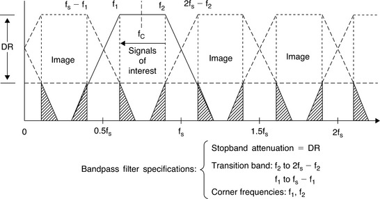
Figure 5-30 shows a signal in the second Nyquist zone centered around a carrier frequency, fc, whose lower and upper frequencies are f1 and f2, respectively. The antialiasing filter is a bandpass filter. The desired dynamic range is DR, which defines the filter stopband attenuation. The upper transition band is f2 to 2fs − f2, and the lower is f1 to fs − f1. As in the case of baseband sampling, the antialiasing filter requirements can be relaxed by proportionally increasing the sampling frequency, but fc must also be increased so that it is always centered in the second Nyquist zone.
Two key equations can be used to select the sampling frequency, fs, given the carrier frequency, fc, and the bandwidth of its signal, Δf. The first is the Nyquist criteria:
The second equation ensures that fc is placed in the center of a Nyquist zone:
where NZ = 1, 2, 3, 4, … and NZ corresponds to the Nyquist zone in which the carrier and its signal fall (see Figure 5-31).
NZ is normally chosen to be as large as possible while still maintaining fs lt; 2Δf. This results in the minimum required sampling rate. If NZ is chosen to be odd, then fc and its signal will fall in an odd Nyquist zone, and the image frequencies in the first Nyquist zone will not be reversed. Tradeoffs can be made between the sampling frequency and the complexity of the antialiasing filter by choosing smaller values of NZ (hence a higher sampling frequency).
As an example, consider a 4 MHz wide signal centered around a carrier frequency of 71 MHz. The minimum required sampling frequency is therefore 8 MSPS. Solving Eq. (5.6) for NZ using fc = 71 MHz and fs = 8 MSPS yields NZ = 18.25. However, NZ must be an integer, so we round 18.25 to the next lowest integer, 18. Solving Eq. (5.6) again for fs yields fs = 8.1143 MSPS. The final values are therefore fs = 8.1143 MSPS, fc = 71 MHz, and NZ = 18.
Now assume that we desire more margin for the antialiasing filter, and we select fs to be 10 MSPS. Solving Eq. (5.6) for NZ, using fc = 71 MHz and fs = 10 MSPS yields NZ = 14.7. We round 14.7 to the next lowest integer, giving NZ = 14. Solving Eq. (5.6) again for fs yields fs = 10.519 MSPS. The final values are therefore fs = 10.519 MSPS, fc = 71 MHz, and NZ = 14.
The above iterative process can also be carried out starting with fs and adjusting the carrier frequency to yield an integer number for NZ.
1 Nyquist H. Certain Factors Affecting Telegraph Speed. Bell System Technical Journal. 1924;Vol. 3:324–346. April
2 Nyquist H. Certain Topics in Telegraph Transmission Theory. A.I.E.E. Transactions. 1928;Vol. 47:617–644. April
3 Hartley R.V.L. Transmission of Information. Bell System Technical Journal. 1928;Vol. 7:535–563. July
4 Shannon C.E. A Mathematical Theory of Communication. Bell System Technical Journal. 1948;Vol. 27:379–423. Julyand October 1948, pp. 623–656.
5 TTE, Inc., 11652 Olympic Blvd., Los Angeles, CA 90064, http://www.tte.com.
