Chapter 7. Passive Devices
An important factor in the success of today’s RF integrated circuits has been the ability to incorporate numerous on-chip passive devices, thus reducing the number of off-chip components. Of course, some integrated passive devices, especially in CMOS technology, exhibit a lower quality than their external counterparts. But, as seen throughout this book, we now routinely use hundreds of such devices in RF transceiver design—an impractical paradigm if they were placed off-chip.
This chapter deals with the analysis and design of integrated inductors, transformers, varactors, and constant capacitors. The outline of the chapter is shown below.
7.1 General Considerations
While analog integrated circuits commonly employ resistors and capacitors, RF design demands additional passive devices, e.g., inductors, transformers, transmission lines, and varactors. Why do we insist on integrating these devices on the chip? If the entire transceiver requires only one or two inductors, why not utilize bond wires or external components? Let us ponder these questions carefully.
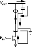
Modern RF design needs many inductors. To understand this point, consider the simple common-source stage shown in Fig. 7.1(a). This topology suffers from two serious drawbacks: (a) the bandwidth at node X is limited to 1/[(RD||rO1)CD], and (b) the voltage headroom trades with the voltage gain, gm1(RD||rO1). CMOS technology scaling tends to improve the former but at the cost of the latter. For example, in 65-nm technology with a 1-V supply, the circuit provides a bandwidth of several gigahertz but a voltage gain in the range of 3 to 4.
Figure 7.1 CS stage with (a) resistive, and (b) inductive loads.
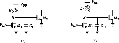
Now consider the inductively-loaded stage depicted in Fig. 7.1(b). Here, LD resonates with CD, allowing operation at much higher frequencies (albeit in a narrow band). Moreover, since LD sustains little dc voltage drop, the circuit can comfortably operate with low supply voltages while providing a reasonable voltage gain (e.g., 10). Owing to these two key properties, inductors have become popular in RF transceivers. In fact, the ability to integrate inductors has encouraged RF designers to utilize them almost as extensively as other devices such as resistors and capacitors.
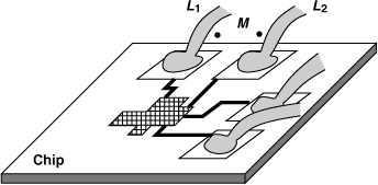
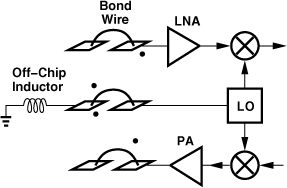
In addition to cost penalties, the use of off-chip devices entails other complications. First, the bond wires and package pins connecting the chip to the outside world may experience significant coupling (Fig. 7.2), creating crosstalk between different parts of the transceiver.
Figure 7.2 Coupling between bond wires.
Second, external connections introduce parasitics that become significant at higher frequencies. For example, a 1-nH bond wire inductance considerably alters the behavior of gigahertz circuits. Third, it is difficult to realize differential operation with external loads because of the poor control of the length of bond wires.
Despite the benefits of integrated components, a critical challenge in RF microelectronics has been how to design high-performance circuits with relatively poor passive devices. For example, on-chip inductors exhibit a lower quality factor than their off-chip counterparts, leading to higher “phase noise” in oscillators (Chapter 8). The RF designer must therefore seek new oscillator topologies that produce a low phase noise even with a moderate inductor Q.
Modeling Issues
Unlike integrated resistors and parallel-plate capacitors, which can be characterized by a few simple parameters, inductors and some other structures are much more difficult to model. In fact, the required modeling effort proves a high barrier to entry into RF design: one cannot add an inductor to a circuit without an accurate model, and the model heavily depends on the geometry, the layout, and the technology’s metal layers (which is the thickest).
It is for these considerations that we devote this chapter to the analysis and design of passive devices.
7.2 Inductors
7.2.1 Basic Structure
Integrated inductors are typically realized as metal spirals (Fig. 7.4). Owing to the mutual coupling between every two turns, spirals exhibit a higher inductance than a straight line having the same length. To minimize the series resistance and the parasitic capacitance, the spiral is implemented in the top metal layer (which is the thickest).
Figure 7.4 Simple spiral inductor.

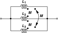
Equation (7.1) suggests that the total inductance rises in proportion to the square of the number of turns. In fact, we prove in Problem 7.1 that the inductance expression for an N-turn structure contains N(N + 1)/2 terms. However, two factors limit the growth rate as a function of N: (a) due to the geometry’s planar nature, the inner turns are smaller and hence exhibit lower inductances, and (b) the mutual coupling factor is only about 0.7 for adjacent turns, falling further for non-adjacent turns. For example, in Eq. (7.1), L3 is quite smaller than L1, and M13 quite smaller than M12. We elaborate on these points in Example 7.4.
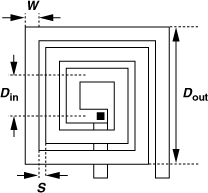
A two-dimensional square spiral is fully specified by four quantities (Fig. 7.5): the outer dimension, Dout, the line width, W, the line spacing, S, and the number of turns, N.1 The inductance primarily depends on the number of turns and the diameter of each turn, but the line width and spacing indirectly affect these two parameters.
Figure 7.5 Various dimensions of a spiral inductor.
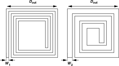
Compared with transistors and resistors, inductors typically have much greater dimensions (“foot prints”), resulting in a large chip area and long interconnects traveling from one block to another. It is therefore desirable to minimize the outer dimensions of inductors. For a given inductance, this can be accomplished by (a) decreasing W [Fig. 7.7(a)], or (b) increasing N [Fig. 7.7(b)]. In the former case, the line resistance rises, degrading the inductor quality. In the latter case, the mutual coupling between the sides of the innermost turns reduces the inductance because opposite sides carry currents in opposite directions. As shown in Fig. 7.7(b), the two opposite legs of the innermost turn produce opposing magnetic fields, partially cancelling each other’s inductance.
Figure 7.7 Effect of (a) reducing the outer dimension and the line width, or (b) reducing the outer dimension and increasing the number of turns.
Figure 7.8 Coupling factor between two straight lines as a function of their normalized spacing.
Solution:
Even for the basic inductor structure of Fig. 7.5, we must answer a number of questions: (1) How are the inductance, the quality factor, and the parasitic capacitance of the structure calculated? (2) What trade-offs do we face in the choice of these values? (3) What technology and inductor parameters affect the quality factor? These questions are answered in the context of inductor modeling in Section 7.2.6.
7.2.2 Inductor Geometries
Our qualitative study of the square spiral inductors reveals some degrees of freedom in the design, particularly the number of turns and the outer dimension. But there are many other inductor geometries that further add to the design space.
Figure 7.9 shows a collection of inductor structures encountered in RF IC design. We investigate the properties of these topologies later in this chapter, but the reader can observe at this point that: (1) the structures in Figs. 7.9(a) and (b) depart from the square shape, (2) the spiral in Fig. 7.9(c) is symmetric, (3) the “stacked” geometry in Fig. 7.9(d) employs two or more spirals in series, (4) the topology in Fig. 7.9(e) incorporates a grounded “shield” under the inductor, and (5) the structure in Fig. 7.9(f) places two or more spirals in parallel.2 Of course, many of these concepts can be combined, e.g., the parallel topology of Fig. 7.9(f) can also utilize symmetric spirals and a grounded shield.
Figure 7.9 Various inductor structures: (a) circular, (b) octagonal, (c) symmetric, (d) stacked, (e) with grounded shield, (f) parallel spirals.

Why are there so many different inductor structures? These topologies have resulted from the vast effort expended on improving the trade-offs in inductor design, specifically those between the quality factor and the capacitance or between the inductance and the dimensions.
While providing additional degrees of freedom, the abundance of the inductor geometries also complicates the modeling task, especially if laboratory measurements are necessary to fine-tune the theoretical models. How many types of inductors and how many different values must be studied? Which structures are more promising for a given circuit application? Facing practical time limits, designers often select only a few geometries and optimize them for their circuit and frequency of interest.
7.2.3 Inductance Equations
With numerous inductors used in a typical transceiver, it is desirable to have closed-form equations that provide the inductance value in terms of the spiral’s geometric properties. Indeed, various inductance expressions have been reported in the literature [1–3], some based on curve fitting and some based on physical properties of inductors. For example, an empirical formula that has less than 10% error for inductors in the range of 5 to 50 nH is given in [1] and can be reduced to the following form for a square spiral:

where Am is the metal area (the shaded area in Fig. 7.5) and Atot is the total inductor area (![]() in Fig. 7.5). All units are metric.
in Fig. 7.5). All units are metric.
Solution:
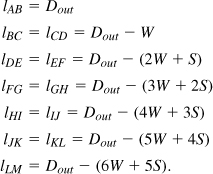
Figure 7.10 Spiral inductor for calculation of line length.
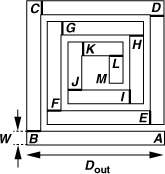
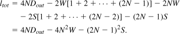
Since ltot ![]() S, we can add one S to the right-hand side so as to simplify the expression:
S, we can add one S to the right-hand side so as to simplify the expression:
![]()
![]()
An interesting property of inductors is that, for a given wire length, width, and spacing, their inductance is a weak function of the number of turns. This can be seen by finding Dout from (7.12), noting that ![]() , and manipulating (7.2) as follows:
, and manipulating (7.2) as follows:
We observe that N appears only within the square brackets in the denominator, in two terms varying in opposite directions, with the result raised to the power of 1/3. For example, if ltot = 2000 μm, W = 4 μm, and S = 0.5 μm, then as N varies from 2 to 3 to 4 to 5, then inductance rises from 3.96 nH to 4.47 nH to 4.83 nH to 4.96 nH, respectively. In other words, a given length of wire yields roughly a constant inductance regardless of how it is “wound.”3 The key point here is that, since this length has a given series resistance (at low frequencies), the choice of N only mildly affects the Q (but can save area).
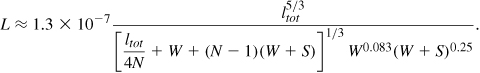
Figure 7.11 plots the inductance predicted by the simulator ASITIC (described below) as N varies from 2 to 6 and the total wire length remains at 2000 μm.4 We observe that L becomes relatively constant for N > 3. Also, the values produced by ASITIC are lower than those given by Eq. (7.15).
Figure 7.11 Inductance as a function of the number of turns for a given line length.
A number of other expressions have been proposed for the inductance of spirals. For example,
![]()
where Davg = (Dout + Din)/2 in Fig. 7.5 and ρ is the “fill factor” and equal to (Dout − Din)/(Dout + Din) [3]. The α coefficients are chosen as follows [3]:
![]()
![]()
Another empirical expression is given by [3]
![]()
![]()
Accuracy Considerations
The above inductance equations yield different levels of accuracy for different geometries. For example, the measurements on tens of inductors in [3] reveal that Eqs. (7.19) and (7.20) incur an error of about 8% for 20% of the inductors and an error of about 4% for 50% of the inductors. We must then ask: how much error is tolerable in inductance calculations? As observed throughout this book and exemplified by Fig. 7.1(b), inductors must typically resonate with their surrounding capacitances at the desired frequency. Since a small error of ΔL/L shifts the resonance frequency, ω0, by approximately ΔL/(2L) (why?), we must determine the tolerable error in ω0.
The resonance frequency error becomes critical in amplifiers and oscillators, but much more so in the latter. This is because, as seen abundantly in Chapter 8, the design of LC oscillators faces tight trade-offs between the “tuning range” and other parameters. Since the tuning range must encompass the error in ω0, a large error dictates a wider tuning range, thereby degrading other aspects of the oscillator’s performance. In practice, the tuning range of high-performance LC oscillators rarely exceeds ±10%, requiring that both capacitance and inductance errors be only a small fraction of this value, e.g., a few percent. Thus, the foregoing inductance expressions may not provide sufficient accuracy for oscillator design.
Another issue with respect to inductance equations stems from the geometry limitations that they impose. Among the topologies shown in Fig. 7.9, only a few lend themselves to the above formulations. For example, the subtle differences between the structures in Figs. 7.9(b) and (c) or the parallel combination of the spirals in Fig. 7.9(f) may yield several percent of error in inductance predictions.
Another difficulty is that the inductance value also depends on the frequency of operation—albeit weakly—while most equations reported in the literature predict the low-frequency value. We elaborate on this dependence in Section 7.2.6.
Field Simulations
With the foregoing sources of error in mind, how do we compute the inductance in practice? We may begin with the above approximate equations for standard structures, but must eventually resort to electromagnetic field simulations for standard or nonstandard geometries. A field simulator employs finite-element analysis to solve the steady-state field equations and compute the electrical properties of the structure at a given frequency.
A public-domain field simulator developed for analysis of inductors and transformers is called “Analysis and Simulation of Spiral Inductors and Transformers” (ASITIC) [4]. The tool can analyze a given structure and report its equivalent circuit components. While simple and efficient, ASITIC also appears to exhibit inaccuracies similar to those of the above equations [3, 5].5
Following rough estimates provided by formulas and/or ASITIC, we must analyze the structure in a more versatile field simulator. Examples include Agilent’s “ADS,” Sonnet Software’s “Sonnet,” and Ansoft’s “HFSS.” Interestingly, these tools yield slightly different values, partly due to the types of approximations that they make. For example, some do not accurately account for the thickness of the metal layers. Owing to these discrepancies, RF circuits sometimes do not exactly hit the targeted frequencies after the first fabrication, requiring slight adjustments and “silicon iterations.” As a remedy, we can limit our usage to a library of inductors that have been measured and modeled carefully but at the cost of flexibility in design and layout.
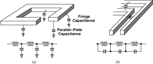
7.2.4 Parasitic Capacitances
As a planar structure built upon a substrate, spiral inductors suffer from parasitic capacitances. We identify two types. (1) The metal line forming the inductor exhibits parallel-plate and fringe capacitances to the substrate [Fig. 7.12(a)]. If a wider line is chosen to reduce its resistance, then the parallel-plate component increases. (2) The adjacent turns also bear a fringe capacitance, which equivalently appears in parallel with each segment [Fig. 7.12(b)].
Figure 7.12 (a) Bottom-plate and (b) interwinding capacitances of an inductor and their models.
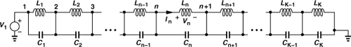
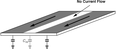
Let us first examine the effect of the capacitance to the substrate. Since in most circuits, one terminal of the inductor is at ac ground, we construct the uniformly-distributed equivalent circuit shown in Fig. 7.13, where each segment has an inductance of Lu. Our objective is to obtain a lumped model for this network. To simplify the analysis, we make two assumptions: (1) each two inductor segments have a mutual coupling of M, and (2) the coupling is strong enough that M can be assumed approximately equal to Lu. While not quite valid, these assumptions lead to a relatively accurate result.
Figure 7.13 Model of an inductor’s distributed capacitance to ground.

The voltage across each inductor segment arises from the current flowing through that segment and the currents flowing through the other segments. That is,
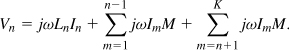
If M ≈ Lu, then

Since this summation is independent of n, we note that all inductor segments sustain equal voltages [6]. The voltage at node n is therefore given by (n/K)V1, yielding an electric energy stored in the corresponding node capacitance equal to
![]()
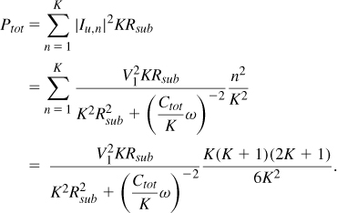
Summing the energies stored on all of the unit capacitances, we have
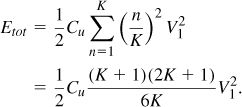
If K → ∞ and Cu → 0 such that KCu is equal to the total wire capacitance, Ctot, then [6]
![]()
revealing that the equivalent lumped capacitance of the spiral is given by Ctot/3 (if one end is grounded).
Let us now study the turn-to-turn (interwinding) capacitance. Using the model shown in Fig. 7.14, where C1 = C2 = ... = CK = CF, we recognize that Eq. (7.22) still applies for it is independent of capacitances. Thus, each capacitor sustains a voltage equal to V1/K, storing an electric energy of
![]()
The total stored energy is given by
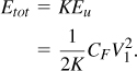
Figure 7.14 Model of an inductor’s turn-to-turn capacitances.
Interestingly, Etot falls to zero as K → ∞ and CF → 0. This is because, for a large number of turns, the potential difference between adjacent turns becomes very small, yielding a small electric energy stored on the CF’s.
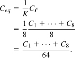
In practice, we can utilize Eq. (7.29) to estimate the equivalent lumped capacitance for a finite number of turns. The following example illustrates this point.
Figure 7.15 (a) Spiral inductor for calculation of turn-to-turn capacitances, (b) circuit model.

Solution:
![]()
The frequency at which an inductor resonates with its own capacitances is called the “self-resonance frequency” (fSR). In essence, the inductor behaves as a capacitor at frequencies above fSR. For this reason, fSR serves as a measure of the maximum frequency at which a given inductor can be used.
![]()
Figure 7.16 (a) Simple tank and (b) behavior of one definition of Q.
Solution:
![]()

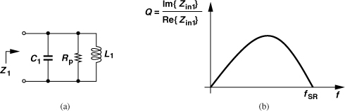
where ![]() . At frequencies well below ωSR, we have Q ≈ Rp/(L1ω), which agrees with our definition in Chapter 2. On the other hand, as the frequency approaches fSR, Q falls to zero [Fig. 7.16(b)]—as if the tank were useless! This definition implies that a general impedance (including additional capacitances due to transistors, etc.) exhibits a Q of zero at resonance. Of course, the tank of Fig. 7.16(a) simply reduces to resistor Rp at fSR, providing a Q of Rp/(L1ωSR) rather than zero. Owing to its meaningless behavior around resonance, the Q definition given by Eq. (7.34) proves irrelevant to circuit design. We return to this point in Section 7.2.6.
. At frequencies well below ωSR, we have Q ≈ Rp/(L1ω), which agrees with our definition in Chapter 2. On the other hand, as the frequency approaches fSR, Q falls to zero [Fig. 7.16(b)]—as if the tank were useless! This definition implies that a general impedance (including additional capacitances due to transistors, etc.) exhibits a Q of zero at resonance. Of course, the tank of Fig. 7.16(a) simply reduces to resistor Rp at fSR, providing a Q of Rp/(L1ωSR) rather than zero. Owing to its meaningless behavior around resonance, the Q definition given by Eq. (7.34) proves irrelevant to circuit design. We return to this point in Section 7.2.6.

7.2.5 Loss Mechanisms
The quality factor, Q, of inductors plays a critical role in various RF circuits. For example, the phase noise of oscillators is proportional to 1/Q2 (Chapter 8), and the voltage gain of “tuned amplifiers” [e.g., the CS stage in Fig. 7.1(b)] is proportional to Q. In typical CMOS technologies and for frequencies up to 5 GHz, a Q of 5 is considered moderate and a Q of 10, relatively high.
We define the Q carefully in Section 7.2.6, but for now we consider Q as a measure of how much energy is lost in an inductor when it carries a sinusoidal current. Since only resistive components dissipate energy, the loss mechanisms of inductors relate to various resistances within or around the structure that carry current when the inductor does.
In this section, we study these loss mechanisms. As we will see, it is difficult to formulate the losses analytically; we must therefore resort to simulations and even measurements to construct accurate inductor models. Nonetheless, our understanding of the loss mechanisms helps us develop guidelines for inductor modeling and design.
Metal Resistance
Suppose the metal line forming an inductor exhibits a series resistance, RS (Fig. 7.17). The Q may be defined as the ratio of the desirable impedance, L1ω0, and the undesirable impedance, RS:
![]()
Figure 7.17 Metal resistance in a spiral inductor.
For example, a 5-nH inductor operating at 5 GHz with an RS of 15.7 Ω has a Q of 10.
Assuming a sheet resistance of 22 mΩ/![]() for the metal, W = 4 μm, and S = 0.5 μm, determine if the above set of values is feasible.
for the metal, W = 4 μm, and S = 0.5 μm, determine if the above set of values is feasible.
Solution:
Recall from our estimates in Section 7.2.3, a 2000-μm long, 4-μm wide wire that is wound into N = 5 turns with S = 0.5 μm provides an inductance of about 4.96 nH. Such a wire consists of 2000/4 = 500 squares and hence has a resistance of 500 × 22 mΩ/![]() = 11 Ω. It thus appears that a Q of 10 at 5 GHz is feasible.
= 11 Ω. It thus appears that a Q of 10 at 5 GHz is feasible.
Unfortunately, the above example portrays an optimistic picture: the Q is limited not only by the (low-frequency) series resistance but also by several other mechanisms. That is, the overall Q may fall quite short of 10. As a rule of thumb, we strive to design inductors such that the low-frequency metal resistance yields a Q about twice the desired value, anticipating that other mechanisms drop the Q by a factor of 2.
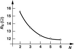
How do we reduce the metal dc resistance for a given inductance? As explained in Section 7.2.3, the total length of the metal wire and the inductance are inextricably related, i.e., for a given W, S, and wire length, the inductance is a weak function of N. Thus, with W and S known, a desired inductance value translates to a certain length and hence a certain dc resistance almost regardless of the choice of N. Figure 7.18 plots the wire resistance of a 5-nH inductor with N = 2 to 6, W = 4 μm, and S = 0.5 μm. In a manner similar to the flattening effect in Fig. 7.11, RS falls to a relatively constant value for N > 3.
Figure 7.18 Metal resistance of an inductor as a function of number of turns.
From the above discussions, we conclude that the only parameter among Dout, S, N, and W that significantly affects the resistance is W. Of course, a wider metal line exhibits less resistance but a larger capacitance to the substrate. Spiral inductors therefore suffer from a trade-off between their Q and their parasitic capacitance. The circuit design limitations imposed by this capacitance are examined in Chapters 5 and 8.
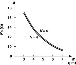
As explained in Example 7.3, a wider metal line yields a smaller inductance value if S, Dout, and N remain constant. In other words, to retain the same inductance while W increases, we must inevitably increase Dout (or N), thereby increasing the length and counteracting the resistance reduction afforded by a wider line. To illustrate this effect, we can design spirals having a given inductance but different line widths and examine the resistance. Figure 7.19 plots RS as a function of W for an inductance of 2 nH and with four or five turns. We observe that RS falls considerably as W goes from 3 μm to about 5 μm but begins to flatten thereafter. In other words, choosing W > 5 μm in this example negligibly reduces the resistance but increases the parasitic capacitance proportionally.
Figure 7.19 Metal resistance of an inductor as a function of line width for different number of turns.
In summary, for a given inductance value, the choice of N has little effect on RS, and a larger W reduces RS to some extent but at the cost of higher capacitance. These limitations manifest themselves particularly at lower frequencies, as shown by the following example.
Solution:
Let us attempt to raise the inductance, hoping that, in Q = L1ω0/RS, L1 can increase at a higher rate than can RS. Indeed, we observe from Eq. (7.15) that ![]() , whereas RS α ltot. For example, if ltot = 8 mm, N = 10, W = 6 μm, and S = 0.5 μm, then Eq. (7.15) yields L ≈ 35 nH. For a sheet resistance of 22 mΩ/
, whereas RS α ltot. For example, if ltot = 8 mm, N = 10, W = 6 μm, and S = 0.5 μm, then Eq. (7.15) yields L ≈ 35 nH. For a sheet resistance of 22 mΩ/![]() , RS = (8000 μm/6 μm) × 22 mΩ/
, RS = (8000 μm/6 μm) × 22 mΩ/![]() = 29.3 Ω. Thus, the Q (due to the dc resistance) reaches 6.75 at 900 MHz. Note, however, that this structure occupies a large area. The reader can readily show that the outer dimension of this spiral is approximately equal to 265 μm.
= 29.3 Ω. Thus, the Q (due to the dc resistance) reaches 6.75 at 900 MHz. Note, however, that this structure occupies a large area. The reader can readily show that the outer dimension of this spiral is approximately equal to 265 μm.
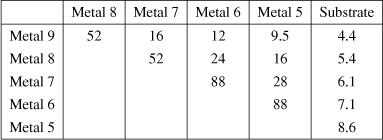
Another approach to reducing the wire resistance is to place two or more metal layers in parallel, as suggested by Fig. 7.9(f). For example, adding a metal-7 and a metal-8 spiral to a metal-9 structure lowers the resistance by about a factor of 2 because metals 7 and 8 are typically half as thick as metal 9. However, the closer proximity of metal 7 to the substrate slightly raises the parasitic capacitance.
Which approach provides a more favorable resistance-capacitance trade-off: widening the metal line of a single layer or placing multiple layers in parallel? We surmise the latter; after all, if W is doubled, the capacitance of a single spiral increases by at least a factor of 2, but if metal-7 and metal-8 structures are placed in parallel with a metal-9 spiral, the capacitance may rise by only 50%. For example, the metal-9-substrate and metal-7-substrate capacitances are around 4 af/μm2 and 6 af/μm2, respectively. The following example demonstrates this point.
Solution:
Since W is reduced from 6 μm to 3 μm, the term (W + S)0.25 in the denominator of Eq. (7.15) falls by a factor of 1.17, requiring a similar drop in ![]() in the numerator so as to obtain L ≈ 35 nH. Iteration yields ltot ≈ 6800 μm. The length and the outer dimension are smaller because the narrower metal line allows a tighter compaction of the turns. With three metal layers in parallel, we assume a sheet resistance of approximately 11 mΩ/
in the numerator so as to obtain L ≈ 35 nH. Iteration yields ltot ≈ 6800 μm. The length and the outer dimension are smaller because the narrower metal line allows a tighter compaction of the turns. With three metal layers in parallel, we assume a sheet resistance of approximately 11 mΩ/![]() , obtaining RS = 25 Ω and hence a Q of 7.9 (due to the dc resistance). The parallel combination therefore yields a higher Q.
, obtaining RS = 25 Ω and hence a Q of 7.9 (due to the dc resistance). The parallel combination therefore yields a higher Q.
Skin Effect
At high frequencies, the current through a conductor prefers to flow at the surface. If the overall current is viewed as many parallel current components, these components tend to repel each other, migrating away so as to create maximum distance between them. This trend is illustrated in Fig. 7.21. Flowing through a smaller cross section area, the high-frequency current thus faces a greater resistance. The actual distribution of the current follows an exponential decay from the surface of the conductor inward, J(s) = J0 exp (−x/δ), where J0 denotes the current density (in A/m2) at the surface, and δ is the “skin depth.” The value of δ is given by

where f denotes the frequency, μ the permeability, and σ the conductivity. For example, δ ≈ 1.4 μm at 10 GHz for aluminum. The extra resistance of a conductor due to the skin effect is equal to
![]()
Figure 7.21 Current distribution in a conductor at (a) low and (b) high frequencies.
Parallel spirals can reduce this resistance if the skin depth exceeds the sum of the metal wire thicknesses.
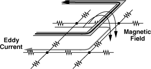
In spiral inductors, the proximity of adjacent turns results in a complex current distribution. As illustrated in Fig. 7.22(a), the current may concentrate near the edge of the wire. To understand this “current crowding” effect, consider the more detailed diagram shown in Fig. 7.22(b), where each turn carries a current of I(t) [7, 8]. The current in one turn creates a time-varying magnetic field, B, that penetrates the other turns, generating loops of current.8 Called “eddy currents,” these components add to I(t) at one edge of the wire and subtract from I(t) at the other edge. Since the induced voltage increases with frequency, the eddy currents and hence the nonuniform distribution become more prominent at higher frequencies.
Figure 7.22 (a) Current distribution in adjacent turns, (b) detailed view of (a).
Based on these observations, [7, 8] derive the following expression for the resistance of a spiral inductor:
where R0 is the dc resistance and the frequency fcrit denotes the onset of current crowding and is given by
![]()
In this equation, R![]() represents the dc sheet resistance of the metal.
represents the dc sheet resistance of the metal.
Solution:
For the single-layer spiral, R![]() = 22 mΩ/
= 22 mΩ/![]() , W = 6 μm, S = 0.5 μm, and hence fcrit = 1.56 GHz. Thus, Reff = 1.03R0 = 30.3 Ω. For the multilayer spiral, R
, W = 6 μm, S = 0.5 μm, and hence fcrit = 1.56 GHz. Thus, Reff = 1.03R0 = 30.3 Ω. For the multilayer spiral, R![]() = 11 mΩ/
= 11 mΩ/![]() , W = 3 μm, S = 0.5 μm, and hence fcrit = 1.68 GHz. We therefore have Reff = 1.03R0 = 26 Ω.
, W = 3 μm, S = 0.5 μm, and hence fcrit = 1.68 GHz. We therefore have Reff = 1.03R0 = 26 Ω.
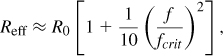
Current crowding also alters the inductance and capacitance of spiral geometries. Since the current is pushed to the edge of the wire, the equivalent diameter of each turn changes slightly, yielding an inductance different from the low-frequency value. Similarly, as illustrated in Fig. 7.23(a), if a conductor carries currents only near the edges, then its middle section can be “carved out” without altering the currents and voltages, suggesting that the capacitance of this section, Cm, is immaterial. From another perspective, Cm manifests itself only if it carries displacement current, which is not possible if the middle section has no current. Based on this observation, [7, 8] approximate the total capacitance, Ctot, to vary inversely proportional to the wire resistance:
![]()
where C0 denotes the low-frequency capacitance.
Figure 7.23 Reduction of capacitance to the substrate as a result of current crowding.
Capacitive Coupling to Substrate
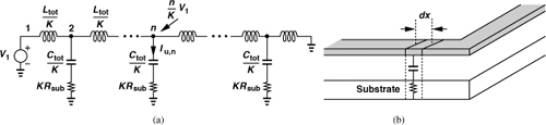
We have seen in our studies that spirals exhibit capacitance to the substrate. As the voltage at each point on the spiral rises and falls with time, it creates a displacement current that flows through this capacitance and the substrate (Fig. 7.24). Since the substrate resistivity is neither zero nor infinity, this flow of current translates to loss in each cycle of the operation, lowering the Q.
Figure 7.24 Substrate loss due to capacitive coupling.

Solution:
Figure 7.25 (a) Distributed model of capacitive coupling to the substrate, (b) diagram showing an infinitesimal section.

For example, if ![]() , then
, then ![]() . Conversely, if
. Conversely, if ![]() , then
, then ![]() .
.
The foregoing example provides insight into the power loss due to capacitive coupling to the substrate. The distributed model of the substrate, however, is not accurate. As depicted in Fig. 7.26(a), since the connection of the substrate to ground is physically far, some of the displacement current flows laterally in the substrate. Lateral substrate currents are more pronounced between adjacent turns [Fig. 7.26(b)] because their voltage difference, V1 − V2, is larger than the incremental drops in Fig. 7.26(a), Vn+1 − Vn. The key point here is that the inductor-substrate interaction can be quantified accurately only if a three-dimensional model is used, but a rare case in practice.
Figure 7.26 Lateral current flow in the substrate (a) under a branch, and (b) from one branch to another.

Magnetic Coupling to the Substrate
The magnetic coupling from an inductor to the substrate can be understood with the aid of basic electromagnetic laws: (1) Ampere’s law states that a current flowing through a conductor generates a magnetic field around the conductor; (2) Faraday’s law states that a time-varying magnetic field induces a voltage, and hence a current if the voltage appears across a conducting material; (3) Lenz’s law states that the current induced by a magnetic field generates another magnetic field opposing the first field.
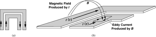
Ampere’s and Faraday’s laws readily reveal that, as the current through an inductor varies with time, it creates an eddy current in the substrate (Fig. 7.27). Lenz’s law implies that the current flows in the opposite direction. Of course, if the substrate resistance were infinity, no current would flow and no loss would occur.
Figure 7.27 Magnetic coupling to the substrate.
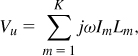
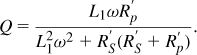
The induction of eddy currents in the substrate can also be viewed as transformer coupling. As illustrated in Fig. 7.28(a), the inductor and the substrate act as the primary and the secondary, respectively. Figure 7.28(b) depicts a lumped model of the overall system, with L1 representing the spiral, M the magnetic coupling, and L2 and Rsub the substrate. It follows that
![]()
Figure 7.28 (a) Modeling of magnetic coupling by transformers, (b) lumped model of (a).

Thus,
![]()
For s = jω,
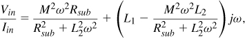
implying that Rsub is transformed by a factor of ![]() and the inductance is reduced by an amount equal to
and the inductance is reduced by an amount equal to ![]() .
.

It is instructive to consider a few special cases of Eq. (7.54). If L1 = L2 = M, then
![]()
indicating that Rsub simply appears in parallel with L1, lowering the Q.
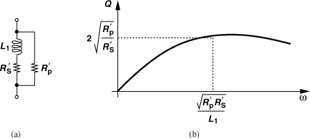
Solution:
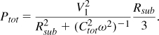
At low frequencies, the Q is given by the dc resistance of the spiral, RS. As the frequency increases, Q = L1ω/RS rises linearly up to a point where skin effect becomes significant [Fig. 7.30(a)]. The Q then increases in proportion to ![]() . At higher frequencies, L1ω
. At higher frequencies, L1ω ![]() RS, and Eq. (7.57) reveals that Rsub shunts the inductor, limiting the Q to
RS, and Eq. (7.57) reveals that Rsub shunts the inductor, limiting the Q to
![]()
Figure 7.30 (a) Inductor model reflecting loss at different frequencies, (b) corresponding Q behavior.
As another special case, suppose Rsub ![]() |L2s|. We can then factor L2s out in Eq. (7.54) and approximate the result as
|L2s|. We can then factor L2s out in Eq. (7.54) and approximate the result as
Thus, as predicted in Example 7.15, the inductance is reduced by an amount equal to M2/L2. Moreover, the substrate resistance is transformed by a factor of ![]() and appears in series with the net inductance.
and appears in series with the net inductance.
7.2.6 Inductor Modeling
Our study of various effects in spiral inductors has prepared us for developing a circuit model that can be used in simulations. Ideally, we wish to obtain a model that retains our physical insights and is both simple and accurate. In practice, some compromise must be made.
It is important to note that (1) both the spiral and the substrate act as three-dimensional distributed structures and can only be approximated by a two-dimensional lumped model; (2) due to skin effect, current-crowding effects, and eddy currents, some of the inductor parameters vary with frequency, making it difficult to fit the model in a broad bandwidth.
Let us begin with a model representing metal losses. As shown in Fig. 7.31(a), a series resistance can embody both low-frequency and skin resistance. With a constant RS, the model is valid for a limited frequency range. As explained in Chapter 2, the loss can alternatively be modeled by a parallel resistance [Fig. 7.31(b)] but still for a narrow range if Rp is constant.
Figure 7.31 Modeling loss by (a) series or (b) parallel resistors.

An interesting observation allows us to combine the models of Figs. 7.31(a) and (b), thus broadening the valid bandwidth. The following example serves as the starting point.
The above observation suggests that we can tailor the frequency dependence of the Q by merging the two models. Depicted in Fig. 7.32(a), such a model partitions the loss between a series resistance and a parallel resistance. A simple approach assigns half of the loss to each at the center frequency of the band:
![]()
![]()
Figure 7.32 (a) Modeling loss by both series and parallel resistors, (b) resulting Q behavior.
In Problem 7.2, we prove that the overall Q of the circuit, defined as Im{Z1}/Re{Z1}, is equal to
Note that this definition of Q is meaningful here because the circuit does not resonate at any frequency. As shown in Fig. 7.32(b), the Q reaches a peak of ![]() at
at ![]() . The choice of
. The choice of ![]() and
and ![]() can therefore yield an accurate variation for a certain frequency range.
can therefore yield an accurate variation for a certain frequency range.
A more general model of skin effect has been proposed by [9] and is illustrated in Fig. 7.33. Suppose a model must be valid only at dc and a high frequency. Then, as shown in Fig. 7.33(a), we select a series resistance, RS1, equal to that due to skin effect and shunt the combination of RS1 and L1 with a large inductor, L2. We then add RS2 in series to model the low-frequency resistance of the wire. At high frequencies, L2 is open and RS1 + RS2 embodies the overall loss; at low frequencies, the network reduces to RS2.
Figure 7.33 (a) Broadband model of inductor, (b) view of a conductor as concentric cylinders, (c) broadband skin effect model.

The above principle can be extended to broadband modeling of skin effect. Depicted in Fig. 7.33(b) for a cylindrical wire, the approach in [9] views the line as a set of concentric cylinders, each having some low-frequency resistance and inductance, arriving at the circuit in Fig. 7.33(c) for one section of the distributed model. Here, the branch consisting of Rj and Lj represents the impedance of cylinder number j. At low frequencies, the current is uniformly distributed through the conductor and the model reduces to R1||R2||...||Rn [9]. As the frequency increases, the current moves away from the inner cylinders, as modeled by the rising impedance of the inductors in each branch. In [9], a constant ratio Rj/Rj+1 is maintained to simplify the model. We return to the use of this model for inductors later in this section.
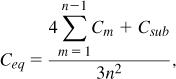
We now add the effect of capacitive coupling to the substrate. Figure 7.34(a) shows a one-dimensional uniformly-distributed model where the total inductance and series resistance are decomposed into n equal segments, i.e., L1 + L2 + ... + Ln = Ltot and RS1 + RS2 + ... + RSn = RS,tot.9 The nodes in the substrate are connected to one another by Rsub1, ..., Rsub,n−1 and to ground by RG1, ..., RGn. The total capacitance between the spiral and the substrate is decomposed into Csub1, ..., Csubn.
Figure 7.34 Distributed inductor model with (a) capacitive and (b) magnetic coupling to substrate.
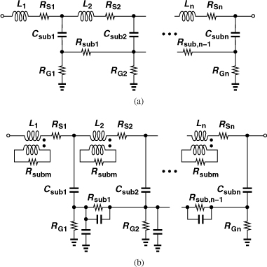
Continuing our model development, we include the magnetic coupling to the substrate. As depicted in Fig. 7.34(b), each inductor segment is coupled to the substrate through a transformer. Proper choice of the mutual coupling and Rsubm allows accurate representation of this type of loss. In this model, the capacitance between the substrate nodes is also included.
While capturing the physical properties of inductors, the model shown in Fig. 7.34(b) proves too complex for practical use. The principal issue is that the numerous parameters make it difficult to fit the model to measured data. We must therefore seek more compact models that more easily lend themselves to parameter extraction and fitting. In the first step, we turn to lumped models. As a simple example, we return to the parallel-series combination of Fig. 7.32(a) and add capacitances to the substrate [Fig. 7.35(a)]. We surmise that ![]() and
and ![]() can represent all of the losses even though they do not physically reflect the substrate loss. We also recall from Section 7.2.4 that an equivalent lumped capacitance, CF, appears between the two terminals. With constant element values, this model is accurate for a bandwidth of about ±20% around the center frequency.
can represent all of the losses even though they do not physically reflect the substrate loss. We also recall from Section 7.2.4 that an equivalent lumped capacitance, CF, appears between the two terminals. With constant element values, this model is accurate for a bandwidth of about ±20% around the center frequency.
Figure 7.35 (a) Compact inductor model, (b) alternative topology.
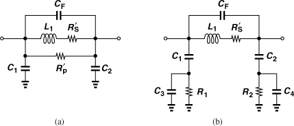
An interesting dilemma arises in the above lumped model. We may choose C1 and C2 to be equal to half of the total capacitance to the substrate, but our analysis in Section 7.2.4 suggests that, if one terminal is grounded, the equivalent capacitance is one-third of the total amount. This is a shortcoming of the lumped model.
Another model that has proved relatively accurate is shown in Fig. 7.35(b). Here, R1 and R2 play a similar role to that of Rp in Fig. 7.35(a). Note that neither model explicitly includes the magnetic coupling to the substrate. The assumption is that the three resistances suffice to represent all of the losses across a reasonable bandwidth (e.g., ±20% around the frequency at which the component values are calculated). A more broadband model is described in [10].
Definitions of Q
In this book, we have encountered several definitions of the Q of an inductor:
![]()
![]()
![]()
In basic physics, the Q of a lossy oscillatory system is defined as
![]()
Additionally, for a second-order tank, the Q can be defined in terms of the resonance frequency, ω0, and the −3-dB bandwidth, ωBW, as
![]()
To make matters more complicated, we can also define the Q of an open-loop system at a frequency ω0 as
![]()
where ϕ denotes the phase of the system’s transfer function (Chapter 8).
Which one of the above definitions is relevant to RF design? We recall from Chapter 2 that Q1 and Q2 model the loss by a single resistance and are equivalent for a narrow bandwidth. Also, from Example 7.7, we discard Q3 because it fails where it matters most: in most RF circuits, inductors operate in resonance (with their own and other circuit capacitances), exhibiting Q3 = 0. The remaining three, namely, Q4, Q5, and Q6, are equivalent for a second-order tank in the vicinity of the resonance frequency.
Before narrowing down the definitions of Q further, we must recognize that, in general, the analysis of a circuit does not require a knowledge of the Q’s of its constituent devices. For example, the inductor model shown in Fig. 7.34(b) represents the properties of the device completely. Thus, the concept of Q has been invented primarily to provide intuition, allowing analysis by inspection as well as the use of certain rules of thumb.
In this book, we mostly deal with only one of the above definitions, Q2. We reduce any resonant network to a parallel RLC tank, lumping all of the loss in a single parallel resistor Rp, and define Q2 = RP/(Lω0). This readily yields the voltage gain of the stage shown in Fig. 7.1(b) as −gm(rO||Rp) at resonance. Moreover, if we wish to compute the Q of a given inductor design at different frequencies, then we add or subtract enough parallel capacitance to create resonance at each frequency and determine Q2 accordingly.
It is interesting to note the following equivalencies for a second-order parallel tank: for Q2 and Q3, we have
![]()
![]()
7.2.7 Alternative Inductor Structures
As illustrated conceptually in Fig. 7.9, many variants of spiral inductors can be envisioned that can potentially raise the Q, lower the parasitic capacitances, or reduce the lateral dimensions. For example, the parallel combination of spirals proves beneficial in reducing the metal resistance. In this section, we deal with several inductor geometries.
Symmetric Inductors
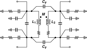
Differential circuits can employ a single symmetric inductor rather than two (asymmetric) spirals (Fig. 7.36). In addition to saving area, a differential geometry (driven by differential signals) also exhibits a higher Q [11]. To understand this property, let us use the model of Fig. 7.35(b) with single-ended and differential stimuli (Fig. 7.37). If in Fig. 7.37(a), we neglect C3 and assume C1 has a low impedance, then the resistance shunting the inductor at high frequencies is approximately equal to R1. That is, the circuit is reduced to that in Fig. 7.37(b).
Figure 7.36 Use of symmetric inductor in a differential circuit.
Figure 7.37 (a) Inductor driven by a single-ended input, (b) simplified model of (a), (c) symmetric inductor driven by differential inputs, (d) simplified model of (c).
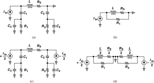
Now, consider the differential arrangement shown in Fig. 7.37(c). The circuit can be decomposed into two symmetric half circuits, revealing that R1 (or R2) appears in parallel with an inductance of L/2 [Fig. 7.37(d)] and hence affects the Q to a lesser extent [11]. In Problem 7.4, we use Eq. (7.62) to compare the Q’s in the two cases. For frequencies above 5 GHz, differential spirals provide a Q of 8 or higher and single-ended structures a Q of about 5 to 6.
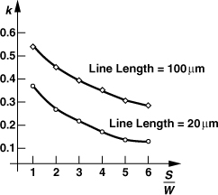
The principal drawback of symmetric inductors is their large interwinding capacitance, a point of contrast to the trend predicted by Eq. (7.29). Consider the arrangement shown in Fig. 7.38(a), where the inductor is driven by differential voltages and viewed as four segments in series. Modeling each segment by an inductor and including the fringe capacitance between the segments, we obtain the network depicted in Fig. 7.38(b). Note that symmetry creates a virtual ground at node 3. This model implies that C1 and C2 sustain large voltages, e.g., as much as Vin/2 if we assume a linear voltage profile from node 1 to node 5 [Fig. 7.38(c)].
Figure 7.38 (a) Symmetric inductor, (b) equivalent circuit, (c) voltage profile along the inductor.
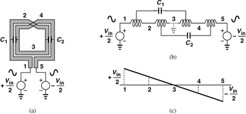
Figure 7.39 (a) Three-turn symmetric inductor, (b) equivalent circuit, (c) voltage profile along the ladder.

Solution:
![]()
![]()
How do we reduce the interwinding capacitance? We can increase the line-to-line spacing, S, but, for a given outer dimension, this results in smaller inner turns and hence a lower inductance. In fact, Eq. (7.15) reveals that L falls as S increases and ltot remains constant, yielding a lower Q. As a rule of thumb, we choose a spacing of approximately three times the minimum allowable value.10 Further increase of S lowers the fringe capacitance only slightly but degrades the Q.
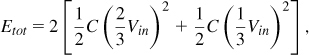
Owing to their higher Q, differential inductors are common in oscillator design, where the Q matters most. They are typically constructed as octagons (a symmetric version of that in Fig. 7.9(b)] because, for a given inductance, an octagonal shape has a shorter length and hence less series resistance than does a square geometry. (Perpendicular sides provide little mutual coupling.) For other differential circuits, such structures can be used, but at the cost of routing complexity. Figure 7.40 illustrates this point for a cascade of two stages. With single-ended spirals on each side, the lines traveling to the next stage can pass between the inductors [Fig. 7.40(a)]. Of course, some spacing is necessary between the lines and the inductors so as to minimize unwanted coupling. On the other hand, with the differential structure, the lines must travel either through the inductor or around it [Fig. 7.40(b)], creating greater coupling than in the former case.
Figure 7.40 Routing of signals to next stage in a circuit using (a) single-ended inductors, (b) a symmetric inductor.
Figure 7.41 Load inductors in a differential pair with (a) mirror symmetry and (b) step symmetry.
Solution:
![]()
where M denotes the mutual coupling between L1 and L2. With a small spacing between the spirals, the mutual coupling factor, k, may reach roughly 0.25, yielding ![]() if L1 = L2 = L. In other words, Leq is 25% less than L1 + L2, exhibiting a lower Q. For k to fall to a few percent, the spacing between L1 and L2 must exceed approximately one-half of the outer dimension of each.
if L1 = L2 = L. In other words, Leq is 25% less than L1 + L2, exhibiting a lower Q. For k to fall to a few percent, the spacing between L1 and L2 must exceed approximately one-half of the outer dimension of each.
![]()
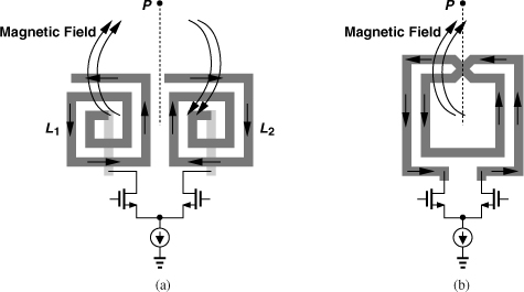
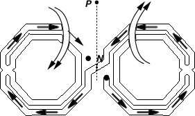
Another important difference between two single-ended inductors and one differential inductor is the amount of signal coupling that they inflict or incur. Consider the topology of Fig. 7.42(a) and a point P on its axis of symmetry. Using the right-hand rule, we observe that the magnetic field due to L1 points into the page at P and that due to L2 out of the page. The two fields therefore cancel along the axis of symmetry. By contrast, the differential spiral in Fig. 7.42(b) produces a single magnetic field at P and hence coupling to other devices even on the line of symmetry.11 This issue is particularly problematic in oscillators: to achieve a high Q, we wish to use symmetric inductors but at the cost of making the circuit more sensitive to injection-pulling by the power amplifier.
Figure 7.42 Magnetic coupling along the axis of symmetry with (a) single-ended inductors and (b) a symmetric inductor.
Inductors with Ground Shield
In our early study of substrate loss in Section 7.2.5, we contemplated the use of a grounded shield below the inductor. The goal was to allow the displacement current to flow through a low resistance to ground, thus avoiding the loss due to electric coupling to the substrate. But we observed that eddy currents in a continuous shield drastically reduce the inductance and the Q.
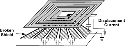
We now observe that the shield can provide a low-resistance termination for electric field lines even if it is not continuous. As illustrated in Fig. 7.44 [13], a “patterned” shield, i.e., a plane broken periodically in the direction perpendicular to the flow of eddy currents, receives most of the electric field lines without reducing the inductance. A small fraction of the field lines sneak through the gaps in the shield and terminate on the lossy substrate. Thus, the width of the gaps must be minimized.
Figure 7.44 Inductor with patterned ground shield.
It is important to note that the patterned ground shield only reduces the effect of capacitive coupling to the substrate. The eddy currents resulting from magnetic coupling continue to flow through the substrate as Faraday and Lenz have prescribed.
The use of a patterned shield may increase the Q by 10 to 15% [13], but this improvement depends on many factors and has thus been inconsistent in different reports [14]. The factors include single-ended versus differential operation, the thickness of the metal, and the resistivity of the substrate. The improvement comes at the cost of higher capacitance. For example, if the inductor is realized in metal 9 and the shield in metal 1, then the capacitance rises by about 15%. One can utilize a patterned n+ region in the substrate as the shield to avoid this capacitance increase, but the measurement results have not been consistent.
The other difficulty with patterned shields is the additional complexity that they introduce in modeling and layout. The capacitance to the shield and the various losses now require much lengthier electromagnetic simulations.
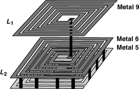
Stacked Inductors
At frequencies up to about 5 GHz, inductor values encountered in practice fall in the range of five to several tens of nanohenries. If realized as a single spiral, such inductors occupy a large area and lead to long interconnects between the circuit blocks. This issue can be resolved by exploiting the third dimension, i.e., by stacking spirals. Illustrated in Fig. 7.45, the idea is to place two or more spirals in series, obtaining a higher inductance not only due to the series connection but also as a result of strong mutual coupling. For example, the total inductance in Fig. 7.45 is given by
![]()
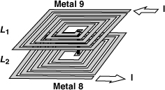
Since the lateral dimensions of L1 and L2 are much greater than their vertical separation, L1 and L2 exhibit almost perfect coupling, i.e., M ≈ L1 = L2 and Ltot ≈ 4L1. Similarly, n stacked spirals operating in series raise the total inductance by approximately a factor of n2.
In reality, the multiplication factor of stacked square inductors is less than n2 because the legs of one inductor that are perpendicular to the legs of the other provide no mutual coupling. For example, a stack of two raises the inductance by about a factor of 3.5 [6]. The factor is closer to n2 for octagonal spirals and almost equal to n2 for circular structures.
In addition to the capacitance to the substrate and the interwinding capacitance, stacked inductors also contain one between the spirals [Fig. 7.46(a)].
Figure 7.46 Equivalent capacitance for a stack of (a) metal-9 and metal-8, or (b) metal-9 and metal-5 spirals.
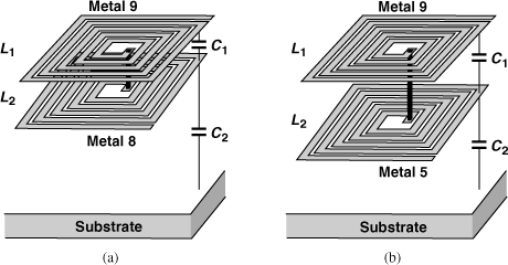
Using an energy-based analysis similar to that in Section 7.2.4, [6] proves that the equivalent lumped capacitance of the inductor shown in Fig. 7.46(a) is equal to
![]()
if the free terminal of L2 is at ac ground.12 Interestingly, the inter-spiral capacitance has a larger weighting factor than the capacitance to the substrate does. For this reason, if L2 is moved to lower metal layers [Fig. 7.46(b)], Ceq falls even though C2 rises. Note that the total inductance remains approximately constant so long as the lateral dimensions are much greater than the vertical spacing between L1 and L2.
For n stacked spirals, it can be proved that
where Cm denotes each inter-spiral capacitance [6].
How does stacking affect the Q? We may surmise that the “resistance-free” coupling, M, among the spirals raises the inductance without increasing the resistance. However, M also exists among the turns of a single, large spiral. More fundamentally, for a given inductance, the total wire’s length is relatively constant and independent of how the wire is wound. For example, the single-spiral 4.96-nH inductor studied above has a total length of 2000 μm and the double-spiral stacked structure in Example 7.23, 1560 μm. But, with a more realistic multiplication factor of 3.5 for the inductance of two stacked spirals, the total length grows to about 1800 μm. We now observe that since the top metal layer is typically thicker than the lower layers, stacking tends to increase the series resistance and hence decrease the Q. The issue can be remedied by placing two or more lower spirals in parallel. Figure 7.47 shows an example where a metal-9 spiral is in series with the parallel combination of metal-6 and metal-5 spirals. Of course, complex current crowding effects at high frequencies require careful electromagnetic field simulations to determine the Q.
Figure 7.47 Stacked inductor using two parallel spirals in metal 6 and metal 5.
7.3 Transformers
Integrated transformers can perform a number of useful functions in RF design: (1) impedance matching, (2) feedback or feedforward with positive or negative polarity, (3) single-ended to differential conversion or vice versa, and (4) ac coupling between stages. They are, however, more difficult to model and design than are inductors.
A well-designed transformer must exhibit the following: (1) low series resistance in the primary and secondary windings, (2) high magnetic coupling between the primary and the secondary, (3) low capacitive coupling between the primary and the secondary, and (4) low parasitic capacitances to the substrate. Some of the trade-offs are thus similar to those of inductors.
7.3.1 Transformer Structures
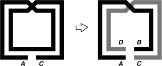
An integrated transformer generally comprises two spiral inductors with strong magnetic coupling. To arrive at “planar” structure, we begin with a symmetric inductor and break it at its point of symmetry (Fig. 7.48). Segments AB and CD now act as mutually-coupled inductors. We consider this structure a 1-to-1 transformer because the primary and the secondary are identical.
Figure 7.48 Transformer derived from a symmetric inductor.
The transformer structure of Fig. 7.48 suffers from low magnetic coupling, an asymmetric primary, and an asymmetric secondary. To remedy the former, the number of turns can be increased [Fig. 7.49(a)] but at the cost of higher capacitive coupling. To remedy the latter, two symmetric spirals can be embedded as shown in Fig. 7.49(b) but with a slight difference between the primary and secondary inductances. The coupling factor in all of the above structures is typically less than 0.8. We study the consequences of this imperfection in the following example.
Figure 7.49 Transformers (a) derived from a three-turn symmetric inductor, (b) formed as two embedded symmetric spirals.
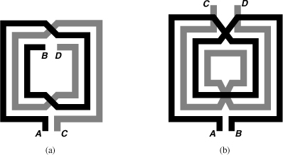
Figure 7.50 Simple transformer model.
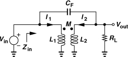
Solution:
![]()
![]()
![]()
suggesting that, since ![]() , the transformer exhibits a low-pass response with a real pole located at
, the transformer exhibits a low-pass response with a real pole located at
Equation (7.88) implies that it is beneficial to reduce L1 and L2 while k remains constant; as L1 and L2 (and ![]() ) approach zero,
) approach zero,
![]()
a frequency-independent quantity equal to k if L1 = L2. However, reduction of L1 and L2 also lowers the input impedance, Zin, in Fig. 7.50. For example, if CF = 0, we have from Eq. (7.54),
![]()
Thus, the number of primary and secondary turns must be chosen so that Zin is adequately high in the frequency range of interest.
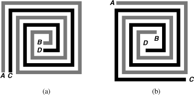
Is it possible to construct planar transformers having a turns ratio greater than unity? Figure 7.51(a) shows an example, where AB has approximately one turn and CD approximately two. We note, however, that the mutual coupling between AB and the inner turn of CD is relatively weak due to the smaller diameter of the latter. Figure 7.51(b) depicts another 1-to-2 example with a stronger coupling factor. In practice, the primary and secondary may require a larger number of turns so as to provide a reasonable input impedance.
Figure 7.51 One-to-two transformers (a) derived from a symmetric inductor, (b) formed as two symmetric inductors.
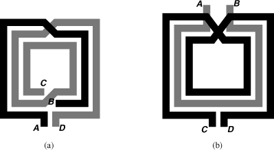
Figure 7.52 shows two other examples of planar transformers. Here, two asymmetric spirals are interwound to achieve a high coupling factor. The geometry of Fig. 7.52(a) can be viewed as two parallel conductors that are wound into turns. Owing to the difference between their lengths, the primary and secondary exhibit unequal inductances and hence a nonunity turns ratio [16]. The structure of Fig. 7.52(b), on the other hand, provides an exact turns ratio of unity [16].
Figure 7.52 (a) Transformer formed as two wires wound together, (b) alternative version with equal primary and secondary lengths.
Transformers can also be implemented as three-dimensional structures. Similar to the stacked inductors studied in Section 7.2.7, a transformer can employ stacked spirals for the primary and the secondary [6]. Figure 7.53(a) shows a 1-to-1 example. It is important to recognize the following attributes: (1) the alignment of the primary and secondary turns results in a slightly higher magnetic coupling factor here than in the planar transformers of Figs. 7.49 and 7.51; (2) unlike the planar structures, the primary and the secondary can be symmetric and identical (except for differences in their capacitances); (3) the overall area occupied by 3D transformers is less than that of their planar counterparts.
Figure 7.53 (a) One-to-one stacked transformer, (b) one-to-two transformer, (c) staggering of turns to reduce coupling capacitance.
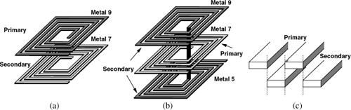
Another advantage of stacked transformers is that they can readily provide a turns ratio higher than unity [6]. Illustrated in Fig. 7.53(b), the idea is to incorporate multiple spirals in series to form the primary or the secondary. Thus, a technology having nine metal layers can afford 1-to-8 transformers! As shown in [6], stacked transformers indeed provide significant voltage or current gain at gigahertz frequencies. This “free” gain can be utilized between stages in a chain.
Stacked transformers must, however, deal with two issues. First, the lower spirals suffer from a higher resistance due to the thinner metal layers. Second, the capacitance between the primary and secondary is larger here than in planar transformers (why?). To reduce this capacitance, the primary and secondary turns can be “staggered,” thus minimizing their overlap [Fig. 7.53(c)] [6]. But this requires a relatively large spacing between the adjacent turns of each inductor, reducing the inductance.
7.3.2 Effect of Coupling Capacitance
The coupling capacitance between the primary and secondary yields different types of behavior with negative and positive mutual (magnetic) coupling factors. To understand this point, we return to the transfer function in Eq. (7.88) and note that, for s = jω, the numerator reduces to
![]()
The first term is always negative, but the polarity of the second term depends on the direction chosen for mutual coupling. Thus, if M > 0, then N(jω) falls to zero at
i.e., the frequency response exhibits a notch at ωz. On the other hand, if M < 0, no such notch exists and the transformer can operate at higher frequencies. We therefore say “noninverting” transformers suffer from a lower speed than do “inverting” transformers [16].
The above phenomenon can also be explained intuitively: the feedforward signal through CF can cancel the signal coupled from L1 to L2. Specifically, the voltage across L2 in Fig. 7.50 contains two terms, namely, L2jωI2 and MjωI1. If, at some frequency, I2 is entirely provided by CF, the former term can cancel the latter, yielding a zero output voltage.
7.3.3 Transformer Modeling
An integrated transformer can be viewed as two inductors having magnetic and capacitive coupling. The inductor models described in Section 7.2.6 therefore directly apply here. Figure 7.54 shows an example, where the primary and secondary are represented by the compact inductor model of Fig. 7.35(b), with the mutual coupling M and coupling capacitor CF added. More details on transformer modeling can be found in [16] and [17]. Due to the complexity of this model, it is difficult to find the value of each component from measurements or field simulations that provide only S-or Y-parameters for the entire structure. In practice, some effort is expended on this type of modeling to develop insight into the transformer’s limitations, but an accurate representation may require that the designer directly use the S-or Y-parameters in circuit simulations. Unfortunately, circuit simulators sometimes face convergence difficulties with these parameters.
Figure 7.54 Transformer model.
7.4 Transmission Lines
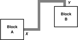
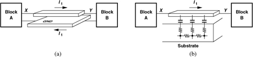
Integrated transmission lines (T-lines) are occasionally used in RF design. It is instructive to consider a few examples of T-line applications. Suppose a long wire carries a high-frequency signal from one circuit block to another (Fig. 7.55). The wire suffers from inductance, capacitance, and resistance. If the width of the wire is increased so as to reduce the inductance and series resistance, then the capacitance to the substrate rises. These parasitics may considerably degrade the signal as the frequency exceeds several gigahertz.
Figure 7.55 Two circuit blocks connected by a long wire.
Solution:
Figure 7.56 (a) Current return path through a ground plane, (b) poor definition of current return path.
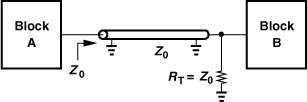
If the long wire in Fig. 7.55 is replaced with a T-line and the input port of block B is modified to match the T-line, then the above issues are alleviated. As illustrated in Fig. 7.57, the line inductance and capacitance no longer degrade the signal, and the T-line ground plane not only provides a low-impedance path for the returning current but minimizes the interaction of the signal with the substrate. The line resistance can also be lowered but with a trade-off (Section 7.4.1).
Figure 7.57 Two circuit blocks connected by a T-line.
As another example of T-line applications, recall from Chapter 2 that a T-line having a short-circuit termination acts as an inductor if it is much shorter than a wavelength. Thus, T-lines can serve as inductive loads (Fig. 7.58).
Figure 7.58 T-line serving as a load inductor.

How does the Q of T-line inductors compare with that of spiral structures? For frequencies as high as several tens of gigahertz, the latter provide a higher Q because of the mutual coupling among their turns. For higher frequencies, it is expected that the former become superior, but actual measured data supporting this prediction are not available—at least in CMOS technology.
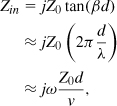
T-lines can also transform impedances. As mentioned in Chapter 2, a line of length d that is terminated with a load impedance of ZL exhibits an input impedance of
![]()
where β = 2π/λ and Z0 is the characteristic impedance of the line. For example, if d = λ/4, then ![]() , i.e., a capacitive load can be transformed to an inductive component. Of course, the required quarter-wave length becomes practical in integrated circuits only at millimeter-wave frequencies.
, i.e., a capacitive load can be transformed to an inductive component. Of course, the required quarter-wave length becomes practical in integrated circuits only at millimeter-wave frequencies.
7.4.1 T-Line Structures
Among various T-line structures developed in the field of microwaves, only a few lend themselves to integration. When choosing a geometry, the RF IC designer is concerned with the following parameters: loss, characteristic impedance, velocity, and size.
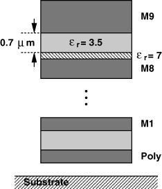
Before studying T-line structures, let us briefly look at the back end of CMOS processes. As exemplified by Fig. 7.60, a typical process provides a silicided polysilicon layer and about nine metal layers. The high sheet resistance, Rsh, of poly (10 to 20 Ω/![]() ) makes it a poor conductor. Each of the lower metal layers has a thickness of approximately 0.3 μm and an Rsh of 60 to 70 mΩ/
) makes it a poor conductor. Each of the lower metal layers has a thickness of approximately 0.3 μm and an Rsh of 60 to 70 mΩ/![]() . The top layer has a thickness of about 0.7 to 0.8 μm and an Rsh of 25 to 30 mΩ/
. The top layer has a thickness of about 0.7 to 0.8 μm and an Rsh of 25 to 30 mΩ/![]() . Between each two consecutive metal layers lie two dielectric layers: a 0.7-μm layer with
. Between each two consecutive metal layers lie two dielectric layers: a 0.7-μm layer with ![]() r ≈ 3.5 and a 0.1-μm layer with
r ≈ 3.5 and a 0.1-μm layer with ![]() r ≈ 7.
r ≈ 7.
Figure 7.60 Typical back end of a CMOS process.
Microstrip
A natural candidate for integrated T-lines is the “microstrip” structure. Depicted in Fig. 7.61, it consists of a signal line realized in the topmost metal layer and a ground plane in a lower metal layer. An important attribute of this topology is that it can have minimal interaction between the signal line and the substrate. This is accomplished if the ground plane is wide enough to contain most of the electric field lines emanating from the signal wire. As a compromise between field confinement and the dimensions of the T-line, we choose WG ≈ 3WS.
Figure 7.61 Microstrip structure.

Numerous equations have been developed in the field of microwaves to express the characteristic impedance of microstrips. For example, if the signal line has a thickness of t and a height of h with respect to the ground plane, then
![]()
![]()
For example, if h = 7 μm, t = 0.8 μm, ![]() r = 4, and WS = 4 μm, then Z0 ≈ 86 Ω. Unfortunately, these equations suffer from errors as large as 10%. In practice, electromagnetic field simulations including the back end details are necessary to compute Z0.
r = 4, and WS = 4 μm, then Z0 ≈ 86 Ω. Unfortunately, these equations suffer from errors as large as 10%. In practice, electromagnetic field simulations including the back end details are necessary to compute Z0.
Solution:
From Eq. (7.96), a T-line with ZL = 0 and 2πd ![]() λ provides an input impedance of
λ provides an input impedance of
i.e., an inductance of Leq = Z0d/v = Lud, where v denotes the wave velocity and Lu the inductance per unit length. Since ωres is inversely proportional to ![]() , a 10% error in Leq translates to about a 5% error in ωres.
, a 10% error in Leq translates to about a 5% error in ωres.
The loss of microstrips arises from the resistance of both the signal line and the ground plane. In modern CMOS technologies, metal 1 is in fact thinner than the higher layers, introducing a ground plane loss comparable to the signal line loss.
The loss of a T-line manifests itself as signal attenuation (or bandwidth reduction) if the line simply connects two blocks. With a typical loss of less than 0.5 dB/mm at frequencies of several tens of gigahertz, a microstrip serves this purpose well. On the other hand, if a T-line acts as an inductive load whose Q is critical, then a much lower loss is required. We can readily relate the loss and the Q. Suppose a T-line of unit length exhibits a series resistance of Ru. As shown in Fig. 7.62,
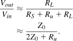
Figure 7.62 Lossy transmission line.

We find the difference between this result and the ideal value and then normalize to 1/2:
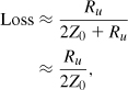
if Ru ![]() 2Z0. Note that this value is expressed in decibels as 20 log(1 − Loss) and the result is negative. A T-line of unit length has a Q of
2Z0. Note that this value is expressed in decibels as 20 log(1 − Loss) and the result is negative. A T-line of unit length has a Q of

Consider a microstrip line 1000 μm long with Z0 = 100 Ω and L = 1 nH. If the signal line is 4 μm wide and has a sheet resistance of 25 mΩ/![]() , determine the loss and the Q at 5 GHz. Neglect skin effect and the loss of the ground plane.
, determine the loss and the Q at 5 GHz. Neglect skin effect and the loss of the ground plane.
Solution:
![]()
In order to reduce the loss of a microstrip, the width of the signal line can be increased (requiring a proportional increase in the width of the ground plane). But such an increase (1) reduces the inductance per unit length (as if multiple signal lines were placed in parallel), and (2) raises the capacitance to the ground plane. Both effects translate to a lower characteristic impedance, ![]() . For example, doubling the signal line width roughly halves Z0.14 Equation (7.97) also reveals this rough dependence.
. For example, doubling the signal line width roughly halves Z0.14 Equation (7.97) also reveals this rough dependence.
The reduction of the characteristic impedance as a result of widening the signal line does make circuit design more difficult. As noted in Fig. 7.57, a properly-terminated T-line loads the driving stage (block A) with a resistance of Z0. Thus, as Z0 decreases, so does the gain of block A. In other words, it is the product of the gain of block A and the inverse loss of the T-line that must be maximized, dictating that the circuit and the line be designed as a single entity.
The resistance of microstrips can also be reduced by stacking metal layers. Illustrated in Fig. 7.63, such a geometry alleviates the trade-off between the loss and the characteristic impedance. Also, stacking allows a narrower footprint for the T-line, thus simplifying the routing and the layout.
Figure 7.63 Microstrip using parallel metal layers for lower loss.

Transmission lines used to transform impedances are prohibitively long for frequencies up to a few tens of gigahertz. However, the relationship ![]() suggests that, if Cu is raised, then the wave velocity can be reduced and so can λ = v/f. Explain the practicality of this idea.
suggests that, if Cu is raised, then the wave velocity can be reduced and so can λ = v/f. Explain the practicality of this idea.
Solution:
The issue is that a higher Cu results in a lower Z0. Thus, the line can be shorter, but it demands a greater drive capability. Moreover, impedance transformation becomes more difficult. For example, suppose a λ/4 line is used to raise ZL to ![]() . This is possible only if Z0 > ZL.
. This is possible only if Z0 > ZL.
Coplanar Lines
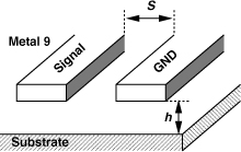
Another candidate for integrated T-lines is the “coplanar” structure. Shown in Fig. 7.64, this geometry realizes both the signal and the ground lines in one plane, e.g., in metal 9. The characteristic impedance of coplanar lines can be higher than that of microstrips because (1) the thickness of the signal and ground lines in Fig. 7.64 is quite small, leading to a small capacitance between them, and (2) the spacing between the two lines can be large, further decreasing the capacitance. Of course, as S becomes comparable with h, more of the electric field lines emanating from the signal wire terminate on the substrate, producing a higher loss. Also, the signal line can be surrounded by ground lines on both sides. The characteristics of coplanar lines are usually obtained by electromagnetic field simulations.
Figure 7.64 Coplanar structure.
The loss reduction techniques described above for microstrips can also be applied to coplanar lines, entailing similar trade-offs. However, coplanar lines have a larger footprint because of their lateral spread, making layout more difficult.
Stripline
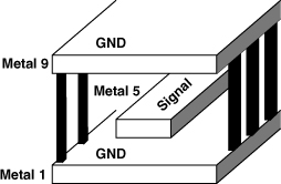
The “stripline” consists of a signal line surrounded by ground planes, thus producing little field leakage to the environment. As an example, a metal-5 signal line can be surrounded by metal-1 and metal-9 planes and vias connecting the two planes (Fig. 7.65). If the vias are spaced closely, the signal line remains shielded in all four directions.
Figure 7.65 Stripline structure.
The stripline exhibits a smaller characteristic impedance than microstrip and coplanar structures do. It is therefore used only where field confinement is essential.
7.5 Varactors
As described in Chapter 8, “varactors” are an essential component of LC VCOs. Varactors also occasionally serve to tune the resonance frequency of narrowband amplifiers.
A varactor is a voltage-dependent capacitor. Two attributes of varactors become critical in oscillator design: (1) the capacitance range, i.e., the ratio of the maximum and minimum capacitances that the varactor can provide, and (2) the quality factor of the varactor, which is limited by the parasitic series resistances within the structure. Interestingly, these two parameters trade with each other in some cases.
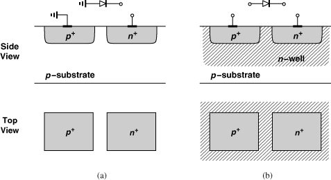
In older generations of RF ICs, varactors were realized as reverse-biased pn junctions. Illustrated in Fig. 7.66(a) is one example where the p-substrate forms the anode and the n+ contact, the cathode. (The p+ contact provides a low-resistance connection to the substrate.) In this case, the anode is “hard-wired” to ground, limiting the design flexibility. A “floating” pn junction can be constructed as shown in Fig. 7.66(b), with an n-well isolating the diode from the substrate and acting as the cathode.
Figure 7.66 PN junction varactor with (a) one terminal grounded, (b) both terminals floating.
Let us examine the capacitance range and Q of pn junctions. At a reverse bias of VD, the junction capacitance, Cj, is given by
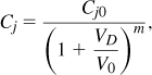
where Cj0 is the capacitance at zero bias, V0 the built-in potential, and m an exponent around 0.3 in integrated structures. We recognize the weak dependence of Cj upon VD. Since V0 ≈ 0.7 to 0.8 V and since VD is constrained to less than 1 V by today’s supply voltages, the term 1 + VD/V0 varies between approximately 1 and 2. Furthermore, an m of about 0.3 weakens this variation, resulting in a capacitance range, Cj,max/Cj,min, of roughly 1.23. In practice, we may allow the varactor to experience some forward bias (0.2 to 0.3 V), thus obtaining a somewhat larger range.
The Q of a pn-junction varactor is given by the total series resistance of the structure. In the floating diode of Fig. 7.66(b), this resistance is primarily due to the n-well and can be minimized by selecting minimum spacing between the n+ and p+ contacts. Moreover, as shown in Fig. 7.67, each p+ region can be surrounded by an n+ ring to lower the resistance in two dimensions.
Figure 7.67 Use of an n+ ring to reduce varactor resistance.

Unlike inductors, transformers, and T-lines, varactors are quite difficult to simulate and model, especially for Q calculations. Consider the displacement current flow depicted in Fig. 7.68(a). Due to the two-dimensional nature of the flow, it is difficult to determine or compute the equivalent series resistance of the structure. This issue arises partly because the sheet resistance of the n-well is typically measured by the foundry for contacts having a spacing greater than the depth of the n-well [Fig. 7.68(b)]. Since the current path in this case is different from that in Fig. 7.68(a), the n-well sheet resistance cannot be directly applied to the calculation of the varactor series resistance. For these reasons, the Q of varactors is usually obtained by measurement on fabricated structures.15
Figure 7.68 Current distribution in a (a) varactor, (b) typical test structure.

In modern RF IC design, MOS varactors have supplanted their pn-junction counterparts. A regular MOSFET exhibits a voltage-dependent gate capacitance (Fig. 7.69), but the nonmonotonic behavior limits the design flexibility. For example, a voltage-controlled oscillator (VCO) employing such a varactor would generate an output frequency that rises and falls as (the average) VGS goes from negative to positive values. This nonmonotonic frequency tuning behavior becomes problematic in phase-locked loop design (Chapter 9).
Figure 7.69 Variation of gate capacitance with VGS.
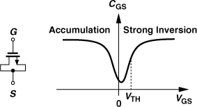
A simple modification of the MOS device avoids the above issues. Called an “accumulation-mode MOS varactor” and shown in Fig. 7.70(a), this structure is obtained by placing an NMOS transistor inside an n-well. If VG < VS, then the electrons in the n-well are repelled from the silicon/oxide interface and a depletion region is formed [Fig. 7.70(b)]. Under this condition, the equivalent capacitance is given by the series combination of the oxide and depletion capacitances. As VG exceeds VS, the interface attracts electrons from the n+ source/drain terminals, creating a channel [Fig. 7.70(c)]. The overall capacitance therefore rises to that of the oxide, behaving as shown in Fig. 7.70(d). (Since the material under the gate is n-type silicon, the concept of strong inversion does not apply here.)
Figure 7.70 (a) MOS varactor, (b) operation with negative gate-source voltage, (c) operation with positive gate-source voltage, (d) resulting C/V characteristic.
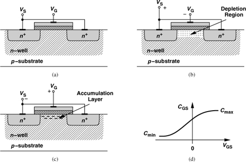
The C/V characteristic of MOS varactors has scaled well with CMOS technology generations, approaching its saturated levels of Cmax and Cmin for VGS ≈ ±0.5 V in 65-nm devices. These varactors therefore operate with low supply voltages better than their pn-junction counterparts.
Another advantage of accumulation-mode MOS varactors is that, unlike pn junctions, they can tolerate both positive and negative voltages. In fact, the characteristic of Fig. 7.70(d) suggests that MOS varactors should operate with positive and negative biases so as to provide maximum tuning range. We pursue this point in VCO design in Chapter 8.
Circuit simulations must somehow incorporate the varactor C/V characteristic of Fig. 7.70(d). In practice, this characteristic is measured on fabricated devices and represented by a table of discrete values. Such a table, however, may introduce discontinuities in the derivatives of the characteristic, creating undesirable artifacts (e.g., a high noise floor) in simulations. It is therefore desirable to approximate the C/V plot by a well-behaved function. The hyperbolic tangent proves useful here for both its saturating behavior and its continuous derivatives. Noting that tanh(±∞) = ± 1, we approximate the characteristic of Fig. 7.70(d) by
![]()
Here, a and V0 allow fitting for the intercept and the slope, respectively, and Cmin and Cmax include the gate-drain and gate-source overlap capacitance.
The above varactor model translates to different characteristics in different circuit simulators! For example, HSPICE predicts a narrower oscillator tuning range than Cadence does. Simulation tools that analyze circuits in terms of voltages and currents (e.g., HSPICE) interpret the nonlinear capacitance equation correctly. On the other hand, programs that represent the behavior of capacitors by charge equations (e.g., Cadence’s Spectre) require that the model be transformed to a Q/V relationship. To this end, we recall the general definition of capacitance from dQ = C(V)dV and write

In other words, the varactor is represented as a two-terminal device whose charge and voltage are related by Eq. (7.112). The simulation tool then computes the current flowing through the varactor as
![]()
The Q of MOS varactors is determined by the resistance between the source and drain terminals.16 As shown in Fig. 7.71(a), this resistance and the capacitance are distributed from the source to the drain and can be approximated by the lumped model depicted in Fig. 7.71(b).
Figure 7.71 (a) Effect of distributed resistance in a varactor, (b) lumped model.

Solution:

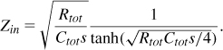
Figure 7.72 (a) Distributed model of a varactor, (b) equivalent circuit for half of the structure, (c) canonical T-line structure.
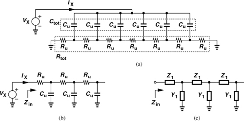
![]()
![]()
The principal difficulty in computing the Q of MOS varactors (placed inside an n-well) is that the resistance between the source and drain cannot be directly computed from the MOS transistor characteristics. As with pn junctions, the Q of MOS varactors is usually obtained from experimental measurements.
How does the Q of MOS varactors vary with the capacitance? In the characteristic of Fig. 7.70(d), as we begin from Cmin, the capacitance is small and the resistance somewhat large (that of n-well). On the other hand, as we approach Cmax, the capacitance rises and the resistance falls. Consequently, equation Q = 1/(RCω) suggests that the Q may remain relatively constant. In practice, however, the Q drops as CGS goes from Cmin to Cmax (Fig. 7.73), indicating that the relative rise in the capacitance is greater than the relative fall in the resistance.
Figure 7.73 Variation of varactor Q with capacitance.

As explained in Chapter 8, it is desirable to maximize the Q of varactors for oscillator design. From our foregoing study of MOS varactors, we conclude that the device length (the distance between the source and drain) must be minimized. Unfortunately, for a minimum channel length, the overlap capacitance between the gate and source/drain terminals becomes a substantial fraction of the overall capacitance, limiting the capacitance range. As illustrated in Fig. 7.74, the overlap capacitance (which is relatively voltage-independent) shifts the C/V characteristic up, yielding a ratio of (Cmax + 2WCov)/(Cmin + 2WCov), where Cmax and Cmin denote the “intrinsic” values, i.e., those without the overlap effect. For a minimum channel length, 2WCov may even be larger than Cmin, thus reducing the capacitance ratio considerably.
Figure 7.74 Effect of overlap capacitance on varactor capacitance range.
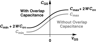
In order to achieve a larger capacitance range, the length of MOS varactors can be increased. In the above example, if the effective channel length grows to 100 nm, then the capacitance ratio reaches (1.7 fF + 0.18 fF)/(0.18 fF) = 10.4. However, the larger sourcedrain resistance results in a lower Q. Since the maximum capacitance goes from 1.03 fF to 1.88 fF and since the channel resistance is doubled, the Q [= 1/(RCω)] falls by a factor of 3.65. In other words, an m-fold increase in the channel length translates to roughly an m2-fold drop in the Q.
The trade-off between the capacitance range and Q of varactors ultimately leads to another between the tuning range and phase noise of LC VCOs. We study this issue in Chapter 8. At frequencies up to about 10 GHz, a channel length of twice the minimum may be chosen so as to widen the capacitance range while retaining a varactor Q much larger than the inductor Q.
7.6 Constant Capacitors
RF circuits employ constant capacitors for various purposes, e.g., (1) to adjust the resonance frequency of LC tanks, (2) to provide ac coupling between stages, or (3) to bypass the supply rail to ground. The critical parameters of capacitors used in RF ICs include the capacitance density (the amount of capacitance per unit area on the chip), the parasitic capacitances, and the Q.
7.6.1 MOS Capacitors
MOSFETs configured as capacitors offer the highest density in integrated circuits because Cox is larger than other capacitances in CMOS processes. However, the use of MOS capacitors entails two issues. First, to provide the maximum capacitance, the device requires a VGS higher than the threshold voltage (Fig. 7.69). A similar “bias” requirement applies to MOS varactors if they are to provide maximum capacitance. Second, the channel resistance limits the Q of MOS capacitors at high frequencies. From Eq. (7.119), we note that the channel resistance is divided by 12 in the lumped model, yielding
![]()
Both of the above issues make MOS capacitors a poor choice for interstage coupling. Depicted in Fig. 7.75(a) is an example, wherein M3 sustains a bias gate-source voltage approximately equal to VDD − VGS2 (why?). With typical values of VDD = 1 V and VGS2 = 0.5V, M3 suffers from a small overdrive voltage and hence a high channel resistance. Moreover, the nonlinearity of the capacitance of M3 may manifest itself if the circuit senses large interferers. For these reasons, MOS capacitors rarely serve as coupling devices.
Figure 7.75 MOS capacitor used as (a) coupling device (b) bypass component.

One application of MOS capacitors is in supply bypass. As illustrated in Fig. 7.75(b), the supply line may include significant bond wire inductance, allowing feedback from the second stage to the first at high frequencies. The bypass capacitor, M3, creates a low impedance between the supply and the ground, suppressing the feedback. In this case, the Q of M3 is still important: if the equivalent series resistance of the device becomes comparable with the reactance of its capacitance, then the bypass impedance may not be low enough to suppress the feedback.
It is important to note that typical MOS models fail to include the channel resistance, Ron, if the source and the drain are shorted. As illustrated in Fig. 7.75(b) for M3, Ron3 is represented as a single lumped component between the two terminals and simply “shorted out” by circuit simulators. For this reason, the designer must compute Ron from I/V characteristics, divide it by 12, and insert the result in series with the MOS capacitor.
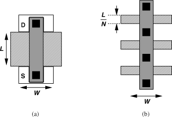
For frequencies up to a few tens of gigahertz, the above decomposition can yield reasonable Q’s (e.g., 5 to 10), allowing the use of MOS capacitors for supply bypass.
The reader is cautioned that very large MOS capacitors suffer from significant gate leakage current, especially with a VGS as high as VDD. This current manifests itself if the system must enter a low-power (standby) mode: the leakage persists as long as VDD is applied, draining the battery.
7.6.2 Metal-Plate Capacitors
If the Q or linearity of MOS capacitors is inadequate, metal-plate capacitors can be used instead. The “parallel-plate” structure employs planes in different metal layers as shown in Fig. 7.77. For maximum capacitance density, all metal layers (and even the poly layer) can be utilized.
Figure 7.77 Parallel-plate capacitor.

The Q and linearity of well-designed parallel-plate capacitors are typically so high that they need not be taken into account. However, even with all metal layers and a poly layer, parallel-plate structures achieve less capacitance density than MOSFETs do. For example, with nine metal layers in 65-nm technology, the former provides a density of about 1.4 fF/μm2 and the latter, 17 fF/μm2.
Parallel-plate geometries also suffer from a parasitic capacitance to the substrate. As illustrated in Fig. 7.79, the capacitance between the lowest plate and the substrate, Cp, divided by the desired capacitance, CAB = C1 + ... + C9, represents the severity of this parasitic. In a typical process, this value reaches 10%, leading to serious difficulties in circuit design.
Figure 7.79 Bottom-plate parasitic capacitance.


To alleviate the above issue, only a few top metal layers can be utilized. For example, a structure consisting of metal 9 through metal 4 has a density of 660 aF/μm2 and a parasitic of 18 aF/μm2, i.e., 2.7%. Of course, the lower density translates to a larger area and more complex routing of signals.
An alternative geometry utilizes the lateral electric field between adjacent metal lines to achieve a high capacitance density. Illustrated in Fig. 7.81, this “fringe” capacitor consists of narrow metal lines with the minimum allowable spacing. This structure is described in Chapter 8.
Figure 7.81 Fringe capacitor structure.
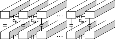
References
[1] J. Craninckx and M. S. J. Steyaert, “A 1.8 GHz CMOS Low Phase Noise Voltage-Controlled Oscillator with Prescaler,” IEEE Journal of Solid-State Circuits, vol. 30, pp. 1474–1482, Dec. 1995.
[2] S. Jenei, B. K. J. C. Nauwelaers, and S. Decoutere, “Physics-Based Closed-Form Inductance Expressions for Compact Modeling of Integrated Spiral Inductors,” IEEE Journal of Solid-State Circuits, vol. 37, pp. 77–80, Jan. 2002.
[3] S. S. Mohan et al., “Simple Accurate Expressions for Planar Spiral Inductances,” IEEE J. Solid-State Circuits, vol. 34, pp. 1419–1424, Oct. 1999.
[4] A. Niknejad and R. G. Meyer, “Analysis, Design, and Optimization of Spiral Inductors and Transformers for Si RF ICs,” IEEE J. Solid-State Circuits, vol. 33, pp. 1470–1481, Oct. 1998.
[5] M. Kraemer, D. Dragomirescu, and R. Plana, “Accurate Electromagnetic Simulation and Measurement of Millimeter-Wave Inductors in Bulk CMOS Technology,” IEEE Topical Meeting on Silison Monolithic Integrated Circuits in RF Systems, pp. 61–64, Jan. 2010.
[6] A. Zolfaghari, A. Y. Chan, and B. Razavi, “Stacked Inductors and 1-to-2 Transformers in CMOS Technology,” IEEE Journal of Solid-State Circuits, vol. 36, pp. 620–628, April 2001.
[7] W. B. Kuhn, “Approximate Analytical Modeling of Current Crowding Effects in Multi-Turn Spiral Inductors,” IEEE RFIC Symp. Dig. Tech. Papers, pp. 271–274, June 2000.
[8] W. B. Kuhn and N. M. Ibrahim, “Analysis of Current Crowding Effects in Multiturn Spiral Inductors,” IEEE Tran. MTT, vol. 49, pp. 31–39, Jan. 2001.
[9] C. S. Yen, Z. Fazarinc, and R. Wheeler, “Time-Domain Skin-Effect Model for Transient Analysis of Lossy Transmission Lines,” Proc. of IEEE, vol. 70, pp. 750–757, July 1982.
[10] Y. Cao et al., “Frequency-Independent Equivalent Circuit Model of On-Chip Spiral Inductors,” Proc. CICC, pp. 217–220, May 2002.
[11] M. Danesh et al., “A Q-Factor Enhancement Technique for MMIC Inductors,” Proc. IEEE Radio Frequency Integrated Circuits Symp., pp. 217–220, April 1998.
[12] N. M. Neihart et al., “Twisted Inductors for Low Coupling Mixed-signal and RF Applications,” Proc. CICC, pp. 575–578, Sept. 2008.
[13] C. P. Yue and S. S. Wong, “On-Chip Spiral Inductors with Patterned Ground Shields for Si-Based RF ICs,” IEEE J. Solid-State Circuits, vol. 33, pp. 743–751, May 1998.
[14] S.-M. Yim, T. Chen, and K. K. O, “The Effects of a Ground Shield on the Characteristics and Performance of Spiral Inductors,” IEEE J. Solid-State Circuits, vol. 37, pp. 237–245, Feb. 2002.
[15] Y. E. Chen et al., “Q-Enhancement of Spiral Inductor with N+-Diffusion Patterned Ground Shields,” IEEE MTT Symp. Dig. Tech. Papers, pp. 1289–1292, 2001.
[16] J. R. Long, “Monolithic Transformers for Silicon RF IC Design,” IEEE J. Solid-State Circuits, vol. 35, pp. 1368–1383, Sept. 2000.
[17] J. R. Long and M. A. Copeland, “The Modeling, Characterization, and Design of Monolithic Inductors for Silicon RF ICs,” IEEE J. Solid-State Circuits, vol. 32, pp. 357–369, March 1997.
[18] S. Ramo, J. R. Whinnery, and T. Van Duzer, Fields and Waves in Communication Electronics, Third Edition, New York: Wiley, 1994.
Problems
7.1. Extend Eq. (7.1) to an N-turn spiral and show that Ltot contains N(N + 1)/2 terms.
7.2. Prove that the Q of the circuit shown in Fig. 7.32(a) is given by Eq. (7.62).
7.3. Prove that for an N-turn spiral inductor, the equivalent interwinding capacitance is given by
![]()
7.4. Using Eq. (7.62), compare the Q’s of the circuits shown in Figs. 7.37(b) and (d).
7.5. Consider the magnetic fields produced by the inductors in Fig. 7.41. Which topology creates less net magnetic field at a point far from the circuit but on its line of symmetry?
7.6. Repeat Example 7.13 for a 5-nH inductor using a line width of 5 μm, a line spacing of 0.5 μm, and four turns. Do the results depend much on the outer diameter?
7.7. For the circuit of Fig. 7.28(a), compute Y11 and find the parallel equivalent resistance. Is the result the same as that shown in Eq. (7.55)?
7.8. Repeat Example 7.19 for four turns. Is it possible to find an expression for N turns?
7.9. Find the input impedance, Zin, in Fig. 7.50.
7.10. Using the capacitance data in Table 7.1, repeat Example 7.25 for an inductor realized as a stack of four metal layers. Assume the inductance is about 3.5 times that of one spiral.
7.11. Suppose an LC VCO (Chapter 8) employs pn-junction varactors. Determine the bounds on the control voltage and the output swings if the varactors must remain reverse-biased.