
Chapter 4. Transceiver Architectures
With the understanding developed in previous chapters of RF design and communication principles, we are now prepared to move down to the transceiver architecture level. The choice of an architecture is determined by not only the RF performance that it can provide but other parameters such as complexity, cost, power dissipation, and the number of external components. In the past ten years, it has become clear that high levels of integration improve the system performance along all of these axes. It has also become clear that architecture design and circuit design are inextricably linked, requiring iterations between the two. The outline of the chapter is shown below.

4.1 General Considerations
The wireless communications environment is often called “hostile” to emphasize the severe constraints that it imposes on transceiver design. Perhaps the most important constraint originates from the limited channel bandwidth allocated to each user (e.g., 200 kHz in GSM). From Shannon’s theorem,1 this translates to a limited rate of information, dictating the use of sophisticated baseband processing techniques such as coding, compression, and bandwidth-efficient modulation.
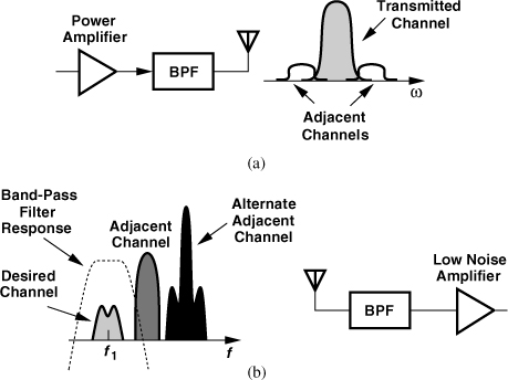
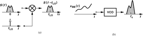
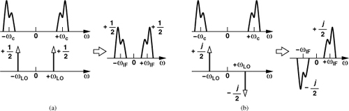
The narrow channel bandwidth also impacts the RF design of the transceiver. As depicted in Fig. 4.1, the transmitter must employ narrowband modulation and amplification to avoid leakage to adjacent channels, and the receiver must be able to process the desired channel while sufficiently rejecting strong in-band and out-of-band interferers.
Figure 4.1 (a) Transmitter and (b) receiver front ends of a wireless system.
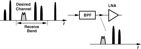
The reader may recall from Chapter 2 that both nonlinearity and noise increase as we add more stages to a cascade. In particular, we recognized that the linearity of a receiver must be high enough to accommodate interferers without experiencing compression or significant intermodulation. The reader may then wonder if we can simply filter the interferers so as to relax the receiver linearity requirements. Unfortunately, two issues arise here. First, since an interferer may fall only one or two channels away from the desired signal (Fig. 4.2), the filter must provide a very high selectivity (i.e., a high Q). If the interferer level is, say, 50–60 dB above the desired signal level, the required value of Q reaches prohibitively high values, e.g., millions. Second, since a different carrier frequency may be allocated to the user at different times, such a filter would need a variable, yet precise, center frequency—a property very difficult to implement.
Figure 4.2 Hypothetical filter to suppress an interferer.

Solution:
![]()
and assume a resonance frequency of ![]() . The magnitude squared of the impedance is thus given by
. The magnitude squared of the impedance is thus given by
![]()
![]()
Channel Selection and Band Selection
The type of filtering speculated above is called “channel-selection filtering” to indicate that it “selects” the desired signal channel and “rejects” the interferers in the other channels. We make two key observations here: (1) all of the stages in the receiver chain that precede channel-selection filtering must be sufficiently linear to avoid compression or excessive intermodulation, and (2) since channel-selection filtering is extremely difficult at the input carrier frequency, it must be deferred to some other point along the chain where the center frequency of the desired channel is substantially lower and hence the required filter Q’s are more reasonable.2
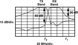
Nonetheless, most receiver front ends do incorporate a “band-select” filter, which selects the entire receive band and rejects “out-of-band” interferers (Fig. 4.3), thereby suppressing components that may be generated by users that do not belong to the standard of interest. We thus distinguish between out-of-band interferers and “in-band interferers,” which are typically removed near the end of the receiver chain.
Figure 4.3 Band-selection filtering.
The front-end band-select (passive) filter suffers from a trade-off between its selectivity and its in-band loss because the edges of the band-pass frequency response can be sharpened only by increasing the order of the filter, i.e., the number of cascaded sections within the filter. Now we note from Chapter 2 that the front-end loss directly raises the NF of the entire receiver, proving very undesirable. The filter is therefore designed to exhibit a small loss (0.5 to 1 dB) and some frequency selectivity.
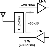
Figure 4.4 plots the frequency response of a typical duplexer,3 exhibiting an in-band loss of about 2 dB and an out-of-band rejection of 30 dB at 20-MHz “offset” with respect to the receive band. That is, an interferer appearing at f1 (20 MHz away from the RX band) is attenuated by only 30 dB, a critical issue in the design of both the receive path and the frequency synthesizer (Chapter 10).
Figure 4.4 Duplexer characteristics.
The in-band loss of the above duplexer in the transmit band also proves problematic as it “wastes” some of the power amplifier output. For example, with 2-dB of loss and a 1-W PA, as much as 370 mW is dissipated within the duplexer—more than the typical power consumed by the entire receive path!
Our observations also indicate the importance of controlled spectral regrowth through proper choice of the modulation scheme and the power amplifier (Chapter 3). The out-of-channel energy produced by the PA cannot be suppressed by the front-end BPF and must be acceptably small by design.
TX-RX Feedthrough
As mentioned in Chapter 3, TDD systems activate only the TX or the RX at any point in time to avoid coupling between the two. Also, even though an FDD system, GSM offsets the TX and RX time slots for the same reason. On the other hand, in full-duplex standards, the TX and the RX operate concurrently. (As explained in Chapter 3, CDMA systems require continual power control and hence concurrent TX and RX operation.) We recognize from the typical duplexer characteristics shown in Fig. 4.4 that the transmitter output at frequencies near the upper end of the TX band, e.g., at f2, is attenuated by only about 50 dB as it leaks to the receiver. Thus, with a 1-W TX power, the leakage sensed by the LNA can reach −20 dBm (Fig. 4.5), dictating a substantially higher RX compression point. For this reason, CDMA receivers must meet difficult linearity requirements.
Figure 4.5 TX leakage in a CDMA transceiver.

4.2 Receiver Architectures
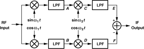
4.2.1 Basic Heterodyne Receivers
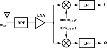
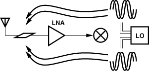
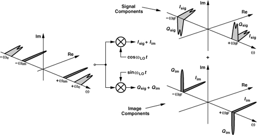
As mentioned above, channel-selection filtering proves very difficult at high carrier frequencies. We must devise a method of “translating” the desired channel to a much lower center frequency so as to permit channel-selection filtering with a reasonable Q. Illustrated in Fig. 4.7(a), the translation is performed by means of a “mixer,” which in this chapter is viewed as a simple analog multiplier. To lower the center frequency, the signal is multiplied by a sinusoid A0 cos ωLOt, which is generated by a local oscillator (LO). Since multiplication in the time domain corresponds to convolution in the frequency domain, we observe from Fig. 4.7(b) that the impulses at ±ωLO shift the desired channel to ±(ωin ± ωLO). The components at ±(ωin + ωLO) are not of interest and are removed by the low-pass filter (LPF) in Fig. 4.7(a), leaving the signal at a center frequency of ωin − ωLO. This operation is called “downconversion mixing” or simply “downconversion.” Due to its high noise, the downconversion mixer is preceded by a low-noise amplifier [Fig. 4.7(c)].
Figure 4.7 (a) Downconversion by mixing, (b) resulting spectra, (c) use of LNA to reduce noise.
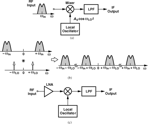
Called the intermediate frequency (IF), the center of the downconverted channel, ωin − ωLO, plays a critical role in the performance. “Heterodyne” receivers employ an LO frequency unequal to ωin and hence a nonzero IF.4
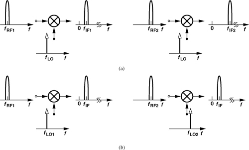
How does a heterodyne receiver cover a given frequency band? For an N-channel band, we can envision two possibilities. (1) The LO frequency is constant and each RF channel is downconverted to a different IF channel [Fig. 4.8(a)], i.e., fIFj = fRFj − fLO. (2) The LO frequency is variable so that all RF channels within the band of interest are translated to a single value of IF [Fig. 4.8(b)], i.e., fLOj = fRFj − fIF. The latter case is more common as it simplifies the design of the IF path; e.g., it does not require a filter with a variable center frequency to select the IF channel of interest and reject the others. However, this approach demands a feedback loop that precisely defines the LO frequency steps, i.e., a “frequency synthesizer” (Chapters 9–11).
Figure 4.8 (a) Constant-LO and (b) constant-IF downconversion mixing.
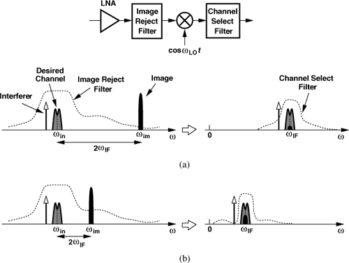
Problem of Image
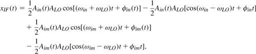
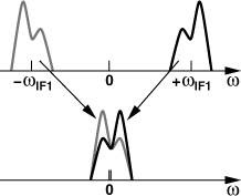
Heterodyne receivers suffer from an effect called the “image.” To understand this phenomenon, let us assume a sinusoidal input and express the IF component as
![]()
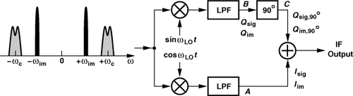
That is, whether ωin−ωLO is positive or negative, it yields the same intermediate frequency. Thus, whether ωin lies above ωLO or below ωLO, it is translated to the same IF. Figure 4.9 depicts a more general case, revealing that two spectra located symmetrically around ωLO are downconverted to the IF. Due to this symmetry, the component at ωim is called the image of the desired signal. Note that ωim = ωin + 2ωIF = 2ωLO − ωin.
Figure 4.9 Problem of image in heterodyne downconversion.
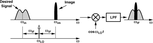
What creates the image? The numerous users in all standards (from police to WLAN bands) that transmit signals produce many interferers. If one interferer happens to fall at ωim = 2ωLO − ωin, then it corrupts the desired signal after downconversion.
While each wireless standard imposes constraints upon the emissions by its own users, it may have no control over the signals in other bands. The image power can therefore be much higher than that of the desired signal, requiring proper “image rejection.”
Solution:
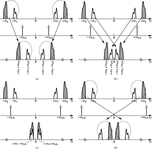
Figure 4.10 Downconversion of two channels for (a) ωLO < ω1, (b) ωLO slightly above ω1, (c) ωLO midway between ω1 and ω2, and (d) ωLO > ω2.
High-Side and Low-Side Injection
In the case illustrated in Fig. 4.9, the LO frequency is above the desired channel. Alternatively, ωLO can be chosen below the desired channel frequency. These two scenarios are called “high-side injection” and “low-side injection,” respectively.5 The choice of one over the other is governed by issues such as high-frequency design issues of the LO, the strength of the image-band interferers, and other system requirements.
Image Rejection
If the choice of the LO frequency leads to an image frequency in a high-interference band, the receiver must incorporate a means of suppressing the image. The most common approach is to precede the mixer with an “image-reject filter.” As shown in Fig. 4.13, the filter exhibits a relatively small loss in the desired band and a large attenuation in the image band, two requirements that can be simultaneously met if 2ωIF is sufficiently large.
Figure 4.13 Image rejection by filtering.
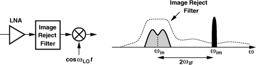
Can the filter be placed before the LNA? More generally, can the front-end band-select filter provide image rejection? Yes, but since this filter’s in-band loss proves critical, its selectivity and hence out-of-band attenuation are inadequate.6 Thus, a filter with high image rejection typically appears between the LNA and the mixer so that the gain of the LNA lowers the filter’s contribution to the receiver noise figure.
The linearity and selectivity required of the image-reject filter have dictated passive, off-chip implementations. Operating at high frequencies, the filters are designed to provide 50-Ω input and output impedances. The LNA must therefore drive a load impedance of 50 Ω, a difficult and power-hungry task.
Image Rejection versus Channel Selection
As noted in Fig. 4.13, the desired channel and the image have a frequency difference of 2ωIF. Thus, to maximize image rejection, it is desirable to choose a large value for ωIF, i.e., a large difference between ωin and ωLO. How large can 2ωIF be? Recall that the premise in a heterodyne architecture is to translate the center frequency to a sufficiently low value so that channel selection by means of practical filters becomes feasible. However, as 2ωIF increases, so does the center of the downconverted channel (ωIF), necessitating a higher Q in the IF filter.
Shown in Fig. 4.14 are two cases corresponding to high and low values of IF so as to illustrate the trade-off. A high IF [Fig. 4.14(a)] allows substantial rejection of the image whereas a low IF [Fig. 4.14(b)] helps with the suppression of in-band interferers. We thus say heterodyne receivers suffer from a trade-off between image rejection and channel selection.
Figure 4.14 Trade-off between image rejection and channel selection for (a) high IF and (b) low IF.
Dual Downconversion
The trade-off between image rejection and channel selection in the simple heterodyne architecture of Fig. 4.14 often proves quite severe: if the IF is high, the image can be suppressed but complete channel selection is difficult, and vice versa. To resolve this issue, the concept of heterodyning can be extended to multiple downconversions, each followed by filtering and amplification. Illustrated in Fig. 4.16, this technique performs partial channel selection at progressively lower center frequencies, thereby relaxing the Q required of each filter. Note that the second downconversion may also entail an image called the “secondary image” here.
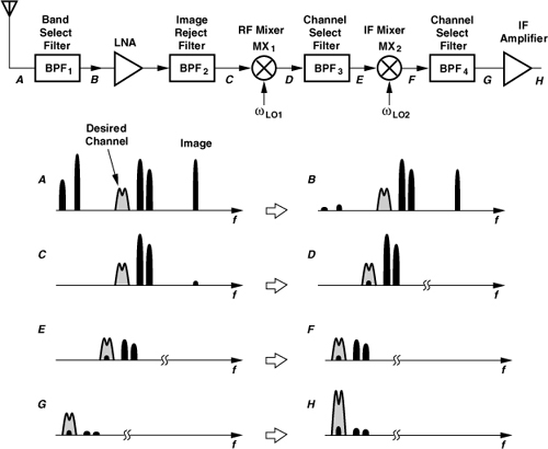
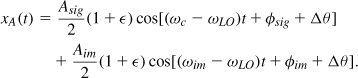
Figure 4.16 also shows the spectra at different points along the cascade. The front-end filter selects the band while providing some image rejection as well. After amplification and image-reject filtering, the spectrum at point C is obtained. A sufficiently linear mixer then translates the desired channel and the adjacent interferers to the first IF (point D). Partial channel selection in BPF3 permits the use of a second mixer with reasonable linearity. Next, the spectrum is translated to the second IF, and BPF4 suppresses the interferers to acceptably low levels (point G). We call MX1 and MX2 the “RF mixer” and the “IF mixer,” respectively.
Recall from Chapter 2 that in a cascade of gain stages, the noise figure is most critical in the front end and the linearity in the back end. Thus, an optimum design scales both the noise figure and the IP3 of each stage according to the total gain preceding that stage. Now suppose the receiver of Fig. 4.16 exhibits a total gain of, say, 40 dB from A to G. If the two IF filters provided no channel selection, then the IP3 of the IF amplifier would need to be about 40 dB higher than that of the LNA, e.g., in the vicinity of +30 dBm. It is difficult to achieve such high linearity with reasonable noise, power dissipation, and gain, especially if the circuit must operate from a low supply voltage. If each IF filter attenuates the in-band interferers to some extent, then the linearity required of the subsequent stages is relaxed proportionally. This is sometimes loosely stated as “every dB of gain requires 1 dB of prefiltering,” or “every dB of prefiltering relaxes the IP3 by 1 dB.”
Mixing Spurs
In the heterodyne receiver of Fig. 4.16, we have assumed ideal RF and IF mixers. In practice, mixers depart from simple analog multipliers, introducing undesirable effects in the receive path. Specifically, as exemplified by the switching mixer studied in Chapter 2, mixers in fact multiply the RF input by a square-wave LO even if the LO signal applied to the mixer is a sinusoid. As explained in Chapter 6, this internal sinusoid/square-wave conversion7 is inevitable in mixer design. We must therefore view mixing as multiplication of the RF input by all harmonics of the LO.8 In other words, the RF mixer in Fig. 4.16 produces components at ωin ± mωLO1 and the IF mixer, ωin ± mωLO1 ± nωLO2, where m and n are integers. For the desired signal, of course, only ωin − ωLO1 − ωLO2 is of interest. But if an interferer, ωint, is downconverted to the same IF, it corrupts the signal; this occurs if
![]()
Called “mixing spurs,” such interferers require careful attention to the choice of the LO frequencies.

The architecture of Fig. 4.16 consists of two downconversion steps. Is it possible to use more? Yes, but the additional IF filters and LO further complicate the design and, more importantly, the mixing spurs arising from additional downconversion mixers become difficult to manage. For these reasons, most heterodyne receivers employ only two downconversion steps.
4.2.2 Modern Heterodyne Receivers
The receiver of Fig. 4.16 employs several bulky, passive (off-chip) filters and two local oscillators; it has thus become obsolete. Today’s architecture and circuit design omits all of the off-chip filters except for the front-end band-select device.
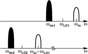
With the omission of a highly-selective filter at the first IF, no channel selection occurs at this point, thereby dictating a high linearity for the second mixer. Fortunately, CMOS mixers achieve high linearities. But the lack of a selective filter also means that the secondary image—that associated with ωLO2—may become serious.
Zero Second IF
To avoid the secondary image, most modern heterodyne receivers employ a zero second IF. Illustrated in Fig. 4.19, the idea is to place ωLO2 at the center of the first IF signal so that the output of the second mixer contains the desired channel with a zero center frequency. In this case, the image is the signal itself, i.e., the left part of the signal spectrum is the image of the right part and vice versa. As explained below, this effect can be handled properly. The key point here is that no interferer at other frequencies can be downconverted as an image to a zero center frequency if ωLO2 = ωIF1.
Figure 4.19 Choice of second LO frequency to avoid secondary image.


What happens if the signal becomes its own image? To understand this effect, we must distinguish between “symmetrically-modulated” and “asymmetrically-modulated” signals. First, consider the generation of an AM signal, Fig. 4.21(a), where a real baseband signal having a symmetric spectrum Sa(f) is mixed with a carrier, thereby producing an output spectrum that remains symmetric with respect to fLO. We say AM signals are symmetric because their modulated spectra carry exactly the same information on both sides of the carrier.10
Figure 4.21 (a) AM signal generation, (b) FM signal generation.
Now, consider an FM signal generated by a voltage-controlled oscillator [Fig. 4.21(b)] (Chapter 8). We note that as the baseband voltage becomes more positive, the output frequency, say, increases, and vice versa. That is, the information in the sideband below the carrier is different from that in the sideband above the carrier. We say FM signals have an asymmetric spectrum. Most of today’s modulation schemes, e.g., FSK, QPSK, GMSK, and QAM, exhibit asymmetric spectra around their carrier frequencies. While the conceptual diagram in Fig. 4.21(b) shows the asymmetry in the magnitude, some modulation schemes may exhibit asymmetry in only their phase.
As exemplified by the spectra in Fig. 4.20, downconversion to a zero IF superimposes two copies of the signal, thereby causing corruption if the signal spectrum is asymmetric. Figure 4.22 depicts this effect more explicitly.
Figure 4.22 Overlap of signal sidebands after second downconversion.

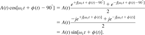
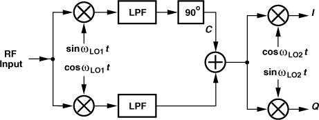
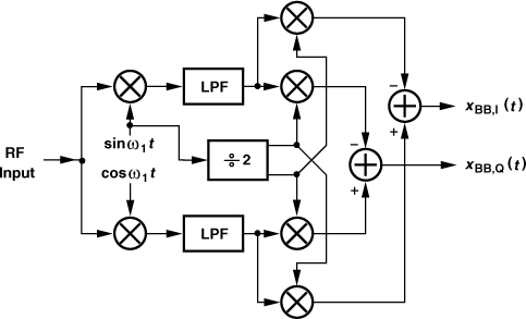
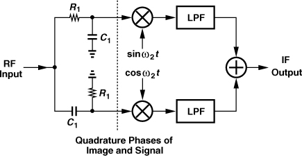
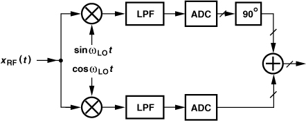
How can downconversion to a zero IF avoid self-corruption? This is accomplished by creating two versions of the downconverted signal that have a phase difference of 90°. Illustrated in Fig. 4.24, “quadrature downconversion” is performed by mixing xIF(t) with the quadrature phases of the second LO (ωLO2 = ωIF1). The resulting outputs, xBB,I(t) and xBB,Q(t), are called the “quadrature baseband signals.” Though exhibiting identical spectra, xBB,I(t) and xBB,Q(t) are separated in phase and together can reconstruct the original information. In Problem 4.8, we show that even an AM signal of the form A(t) cos ωct may require quadrature downconversion.
Figure 4.24 Quadrature downconversion.
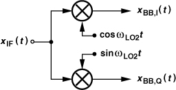
Figure 4.25 shows a heterodyne receiver constructed after the above principles. In the absence of an (external) image-reject filter, the LNA need not drive a 50-Ω load, and the LNA/mixer interface can be optimized for gain, noise, and linearity with little concern for the interface impedance values. However, the lack of an image-reject filter requires careful attention to the interferers in the image band, and dictates a narrow-band LNA design so that the thermal noise of the antenna and the LNA in the image band is heavily suppressed (Example 4.7). Moreover, no channel-select filter is shown at the first IF, but some “mild” on-chip band-pass filtering is usually inserted here to suppress out-of-band interferers. For example, the RF mixer may incorporate an LC load, providing some filtration.
Figure 4.25 Heterodyne RX with quadrature downconversion.

Sliding-IF Receivers
Modern heterodyne receivers entail another important departure from their older counterparts: they employ only one oscillator. This is because the design of oscillators and frequency synthesizers proves difficult and, more importantly, oscillators fabricated on the same chip suffer from unwanted coupling. The second LO frequency is therefore derived from the first by “frequency division.”11 Shown in Fig. 4.26(a) is an example, where the first LO is followed by a ÷2 circuit to generate the second LO waveforms at a frequency of fLO1/2. As depicted in Fig. 4.26(b) and explained in Chapter 10, certain ÷2 topologies can produce quadrature outputs. Figure 4.26(c) shows the spectra at different points in the receiver.
Figure 4.26 (a) Sliding-IF heterodyne RX, (b) divide-by-2 circuit waveforms, (c) resulting spectra.
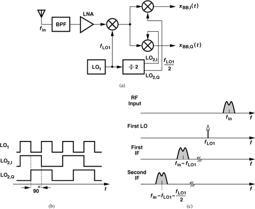
The receiver architecture of Fig. 4.26(a) has a number of interesting properties. To translate an input frequency of fin to a second IF of zero, we must have
![]()
and hence
![]()
That is, for an input band spanning the range [f1 f2], the LO must cover a range of [(2/3)f1 (2/3)f2] (Fig. 4.27). Moreover, the first IF in this architecture is not constant because

Figure 4.27 LO and IF ranges in the sliding-IF RX.
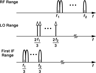
Thus, as fin varies from f1 to f2, fIF1 goes from f1/3 to f2/3 (Fig. 4.27). For this reason, this topology is called the “sliding-IF architecture.” Unlike the conventional heterodyne receiver of Fig. 4.16, where the first IF filter must exhibit a narrow bandwidth to perform some channel selection, this sliding IF topology requires a fractional (or normalized) IF bandwidth12 equal to the RF input fractional bandwidth. This is because the former is given by
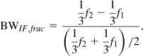
and the latter,
![]()
The sliding-IF architecture may incorporate greater divide ratios in the generation of the second LO from the first. For example, a ÷4 circuit produces quadrature outputs at fLO1/4, leading to the following relationship
![]()
![]()
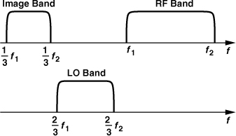
The detailed spectra of such an architecture are studied in Problem 4.1. But we must make two observations here. (1) With a ÷4 circuit, the second LO frequency is equal to fin/5, slightly lower than that of the first sliding-IF architecture. This is desirable because generation of LO quadrature phases at lower frequencies incurs smaller mismatches. (2) Unfortunately, the use of a ÷4 circuit reduces the frequency difference between the image and the signal, making it more difficult to reject the image and even the thermal noise of the antenna and the LNA in the image band. In other words, the choice of the divide ratio is governed by the trade-off between quadrature accuracy and image rejection.
Solution:
Figure 4.29 Image band in an 11g RX with a (a) divide-by-2 circuit, (b) divide-by-4 circuit.
The baseband signals produced by the heterodyne architecture of Fig. 4.26(a) suffer from a number of critical imperfections, we study these effects in the context of direct-conversion architectures.
4.2.3 Direct-Conversion Receivers
In our study of heterodyne receivers, the reader may have wondered why the RF spectrum is not simply translated to the baseband in the first downconversion. Called the “direct-conversion,” “zero-IF,” or “homodyne” architecture,13 this type of receiver entails its own issues but has become popular in the past decade. As explained in Section 4.2.2 and illustrated in Fig. 4.22, downconversion of an asymmetrically-modulated signal to a zero IF leads to self-corruption unless the baseband signals are separated by their phases. The direct-conversion receiver (DCR) therefore emerges as shown in Fig. 4.30, where ωLO = ωin.
Figure 4.30 Direct-conversion receiver.
Three aspects of direct conversion make it a superior choice with respect to heterodyning. First, the absence of an image greatly simplifies the design process. Second, channel selection is performed by low-pass filters, which can be realized on-chip as active circuit topologies with relatively sharp cut-off characteristics. Third, mixing spurs are considerably reduced in number and hence simpler to handle.
The architecture of Fig. 4.30 appears to easily lend itself to integration. Except for the front-end band-select filter, the cascade of stages need not connect to external components, and the LNA/mixer interface can be optimized for gain, noise, and linearity without requiring a 50-Ω impedance. The simplicity of the architecture motivated many attempts in the history of RF design, but it was only in the 1990s and 2000s that integration and sophisticated signal processing made direct conversion a viable choice. We now describe the issues that DCRs face and introduce methods of resolving them. Many of these issues also appear in heterodyne receivers having a zero second IF.
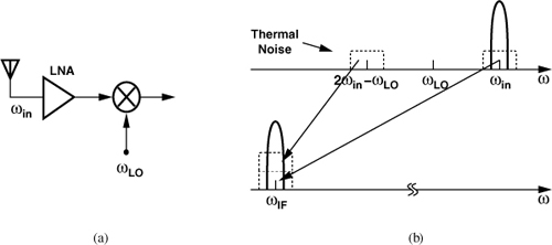
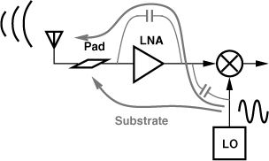
LO Leakage
A direct-conversion receiver emits a fraction of its LO power from its antenna. To understand this effect, consider the simplified topology shown in Fig. 4.31, where the LO couples to the antenna through two paths: (1) device capacitances between the LO and RF ports of the mixer and device capacitances or resistances between the output and input of the LNA; (2) the substrate to the input pad, especially because the LO employs large on-chip spiral inductors. The LO emission is undesirable because it may desensitize other receivers operating in the same band. Typical acceptable values range from −50 to −70 dBm (measured at the antenna).

Does LO leakage occur in heterodyne receivers? Yes, but since the LO frequency falls outside the band, it is suppressed by the front-end band-select filters in both the emitting receiver and the victim receiver.
LO leakage can be minimized through symmetric layout of the oscillator and the RF signal path. For example, as shown in Fig. 4.33, if the LO produces differential outputs and the leakage paths from the LO to the input pad remain symmetric, then no LO is emitted from the antenna. In other words, LO leakage arises primarily from random or deterministic asymmetries in the circuits and the LO waveform.
Figure 4.33 Cancellation of LO leakage by symmetry.
DC Offsets
The LO leakage phenomenon studied above also gives rise to relatively large dc offsets in the baseband, thus creating certain difficulties in the design. Let us first see how the dc offset is generated. Consider the simplified receiver in Fig. 4.34, where a finite amount of in-band LO leakage, kVLO, appears at the LNA input. Along with the desired signal, VRF, this component is amplified and mixed with the LO. Called “LO self-mixing,” this effect produces a dc component in the baseband because multiplying a sinusoid by itself results in a dc term.
Figure 4.34 DC offset in a direct-conversion RX.
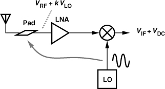
Why is a dc component troublesome? It appears that, if constant, a dc term does not corrupt the desired signal. However, such a component makes the processing of the baseband signal difficult. To appreciate the issue, we make three observations: (1) the cascade of RF and baseband stages in a receiver must amplify the antenna signal by typically 70 to 100 dB; (as a rule of thumb, the signal at the end of the baseband chain should reach roughly 0 dBm.) (2) the received signal and the LO leakage are amplified and processed alongside each other; (3) for an RF signal level of, say, −80 dBm at the antenna, the receiver must provide a gain of about 80 dB, which, applied to an LO leakage of, say, −60 dBm, yields a very large dc offset in the baseband stages. Such an offset saturates the baseband circuits, simply prohibiting signal detection.

Does the problem of dc offsets occur in heterodyne receivers having a zero second IF [Fig. 4.26(a)]? Yes, the leakage of the second LO to the input of the IF mixers produces dc offsets in the baseband. Since the second LO frequency is equal to fin/3 in Fig. 4.26(a), the leakage is smaller than that in direct-conversion receivers,14 but the dc offset is still large enough to saturate the baseband stages or at least create substantial nonlinearity.
The foregoing study implies that receivers having a final zero IF must incorporate some means of offset cancellation in each of the baseband I and Q paths. A natural candidate is a high-pass filter (ac coupling) as shown in Fig. 4.37(a), where C1 blocks the dc offset and R1 establishes proper bias, Vb, for the input of A1. However, as depicted in Fig. 4.37(b), such a network also removes a fraction of the signal’s spectrum near zero frequency, thereby introducing intersymbol interference. As a rule of thumb, the corner frequency of the high-pass filter, f1 = (2πR1C1)−1, must be less than one-thousandth of the symbol rate for negligible ISI. In practice, careful simulations are necessary to determine the maximum tolerable value of f1 for a given modulation scheme.
Figure 4.37 (a) Use of a high-pass filter to remove dc offset, (b) effect on signal spectrum.

The feasibility of on-chip ac coupling depends on both the symbol rate and the type of modulation. For example, the bit rate of 271 kb/s in GSM necessitates a corner frequency of roughly 20–30 Hz and hence extremely large capacitors and/or resistors. Note that the quadrature mixers require four high-pass networks in their differential outputs. On the other hand, 802.11b at a maximum bit rate of 20 Mb/s can operate with a high-pass corner frequency of 20 kHz, a barely feasible value for on-chip integration.
Modulation schemes that contain little energy around the carrier better lend themselves to ac coupling in the baseband. Figure 4.38 depicts two cases for FSK signals: for a small modulation index, the spectrum still contains substantial energy around the carrier frequency, fc, but for a large modulation index, the two frequencies generated by ONEs and ZEROs become distinctly different, leaving a deep notch at fc. If downconverted to baseband, the latter can be high-pass filtered more easily.
Figure 4.38 FSK spectrum with (a) small and (b) large frequency deviation.
A drawback of ac coupling stems from its slow response to transient inputs. With a very low f1 = (2πR1C1)−1, the circuit inevitably suffers from a long time constant, failing to block the offset if the offset suddenly changes. This change occurs if (a) the LO frequency is switched to another channel, hence changing the LO leakage, or (b) the gain of the LNA is switched to a different value, thus changing the reverse isolation of the LNA. (LNA gain switching is necessary to accommodate varying levels of the received signal.) For these reasons, and due to the relatively large size of the required capacitors, ac coupling is rarely used in today’s direct-conversion receivers.
Figure 4.39 (a) Offset cancellation by feedback, (b) resulting frequency response.
Solution:
![]()
![]()
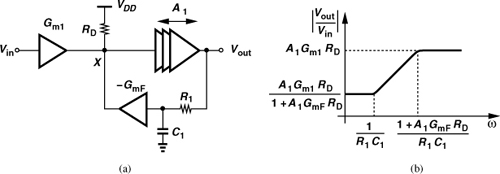
The circuit thus exhibits a pole at −(1 + GmFRDA1)/(R1C1) and a zero at −1/(R1C1) [Fig. 4.39(b)]. The input offset is amplified by a factor of Gm1RDA1/(1 + GmFRDA1) ≈ Gm1/GmF if GmFRDA1 ![]() 1. This gain must remain below unity, i.e., GmF is typically chosen larger than Gm1. Unfortunately, the high-pass corner frequency is given by
1. This gain must remain below unity, i.e., GmF is typically chosen larger than Gm1. Unfortunately, the high-pass corner frequency is given by
![]()
The most common approach to offset cancellation employs digital-to-analog converters (DACs) to draw a corrective current in the same manner as the GmF stage in Fig. 4.39(a). Let us first consider the cascade shown in Fig. 4.40(a), where I1 is drawn from node X and its value is adjusted so as to drive the dc content in Vout to zero.15 For example, if the mixer produces an offset of ΔV at X and the subsequent stages exhibit no offset, then I1 = ΔV/RD with proper polarity. In Fig. 4.39(a), the corrective current provided by GmF is continuously adjusted (even in the presence of signal), leading to the high-pass behavior; we thus seek a method of “freezing” the value of I1 so that it does not affect the baseband frequency response. This requires that I1 be controlled by a register and hence vary in discrete steps. As illustrated in Fig. 4.40(b), I1 is decomposed into units that are turned on or off according to the values stored in the register. For example, a binary word D3D2D1 controls “binary-weighted” current sources 4I, 2I, and I. These current sources form a DAC.
Figure 4.40 (a) Offset cancellation by means of a current source, (b) actual implementation.
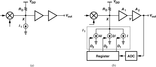
How is the correct value of the register determined? When the receiver is turned on, an analog-to-digital converter (ADC) digitizes the baseband output (in the absence of signals) and drives the register. The entire negative-feedback loop thus converges such that Vout is minimized. The resulting values are then stored in the register and remain frozen during the actual operation of the receiver.
The arrangement of Fig. 4.40(b) appears rather complex, but, with the scaling of CMOS technology, the area occupied by the DAC and the register is in fact considerably smaller than that of the capacitors in Figs. 4.37(a) and 4.39(a). Moreover, the ADC is also used during signal reception.
The digital storage of offset affords other capabilities as well. For example, since the offset may vary with the LO frequency or gain settings before or after the mixer, at power-up the receiver is cycled through all possible combinations of LO and gain settings, and the required values of I1 are stored in a small memory. During reception, for the given LO and gain settings, the value of I1 is recalled from the memory and loaded into the register.
The principal drawback of digital storage originates from the finite resolution with which the offset is cancelled. For example, with the 3-bit DAC in Fig. 4.40(b), an offset of, say, 10 mV at node X, can be reduced to about 1.2 mV after the overall loop settles. Thus, for an A1A2 of, say, 40 dB, Vout still suffers from 120 mV of offset. To alleviate this issue, a higher resolution must be realized or multiple DACs must be tied to different nodes (e.g., Y and Vout) in the cascade to limit the maximum offset.
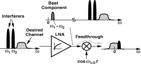
Even-Order Distortion
Our study of nonlinearity in Chapter 2 indicates that third-order distortion results in compression and intermodulation. Direct-conversion receivers are additionally sensitive to even-order nonlinearity in the RF path, and so are heterodyne architectures having a second zero IF.
Suppose, as shown in Fig. 4.41, two strong interferers at ω1 and ω2 experience a nonlinearity such as y(t) = α1x(t) + α2x2(t) in the LNA. The second-order term yields the product of these two interferers and hence a low-frequency “beat” at ω2 − ω1. What is the effect of this component? Upon multiplication by cos ωLOt in an ideal mixer, such a term is translated to high frequencies and hence becomes unimportant. In reality, however, asymmetries in the mixer or in the LO waveform allow a fraction of the RF input of the mixer to appear at the output without frequency translation. As a result, a fraction of the low-frequency beat appears in the baseband, thereby corrupting the downconverted signal. Of course, the beat generated by the LNA can be removed by ac coupling, making the input transistor of the mixer the dominant source of even-order distortion.
Figure 4.41 Effect of even-order distortion on direct conversion.
To understand how asymmetries give rise to direct “feedthrough” in a mixer, first consider the circuit shown in Fig. 4.42(a). As explained in Chapter 2, the output can be written as the product of Vin and an ideal LO, i.e., a square-wave toggling between 0 and 1 with 50% duty cycle, S(t):
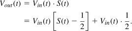
Figure 4.42 (a) Simple mixer, (b) mixer with differential output.
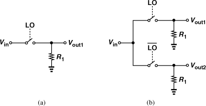
We recognize that S(t) − 1/2 represents a “dc-free” square wave consisting of only odd harmonics. Thus, Vin(t) · [S(t) − 1/2] contains the product of Vin and the odd harmonics of the LO. The second term in (4.26), Vin(t) × 1/2, denotes the RF feedthrough to the output (with no frequency translation).
Next, consider the topology depicted in Fig. 4.42(b), where a second branch driven by ![]() (the complement of LO) produces a second output. Expressing
(the complement of LO) produces a second output. Expressing ![]() as 1 − S(t), we have
as 1 − S(t), we have
![]()
![]()
As with Vout1(t), the second output Vout2(t) contains an RF feedthrough equal to Vin(t) × 1/2 because 1 − S(t) exhibits a dc content of 1/2. If the output is sensed differentially, the RF feedthroughs in Vout1(t) and Vout2(t) are cancelled while the signal components add. It is this cancellation that is sensitive to asymmetries; for example, if the switches exhibit a mismatch between their on-resistances, then a net RF feedthrough arises in the differential output.
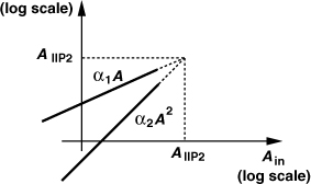
The problem of even-order distortion is critical enough to merit a quantitative measure. Called the “second intercept point” (IP2), such a measure is defined according to a two-tone test similar to that for IP3 except that the output of interest is the beat component rather than the intermodulation product. If Vin(t) = A cos ω1t + A cos ω2t, then the LNA output is given by
Revealing that the beat amplitude grows with the square of the amplitude of the input tones. Thus, as shown in Fig. 4.43, the beat amplitude rises with a slope of 2 on a log scale. Since the net feedthrough of the beat depends on the mixer and LO asymmetries, the beat amplitude measured in the baseband depends on the device dimensions and the layout and is therefore difficult to formulate.
Figure 4.43 Plot illustrating IP2.
Even-order distortion may manifest itself even in the absence of interferers. Suppose in addition to frequency and phase modulation, the received signal also exhibits amplitude modulation. For example, as explained in Chapter 3, QAM, OFDM, or simple QPSK with baseband pulse shaping produce variable-envelope waveforms. We express the signal as xin(t) = [A0 + a(t)] cos[ωct + ϕ(t)], where a(t) denotes the envelope and typically varies slowly, i.e., it is a low-pass signal. Upon experiencing second-order distortion, the signal appears as
![]()
Both of the terms α2A0a(t) and α2a2(t)/2 are low-pass signals and, like the beat component shown in Fig. 4.41, pass through the mixer with finite attenuation, corrupting the down-converted signal. We say even-order distortion demodulates AM because the amplitude information appears as α2A0a(t). This effect may corrupt the signal by its own envelope or by the envelope of a large interferer. We consider both cases below.
How serious is the above phenomenon? Equation (4.35) predicts that the SNR falls to dangerously low levels as the envelope variation becomes comparable with the input IP2. In reality, this is unlikely to occur. For example, if arms = −20 dBm, then A0 is perhaps on the order of −10 to −15 dBm, large enough to saturate the receiver chain. For such high input levels, the gain of the LNA and perhaps the mixer is switched to much lower values to avoid saturation, automatically minimizing the above self-corruption effect.
The foregoing study nonetheless points to another, much more difficult, situation. If the desired channel is accompanied by a large amplitude-modulated interferer, then even-order distortion demodulates the AM component of the interferer, and mixer feedthrough allows it to appear in the baseband. In this case, Eq. (4.34) still applies but the numerator must represent the desired signal, ![]() , and the denominator, the interferer kα2Aintarms:
, and the denominator, the interferer kα2Aintarms:
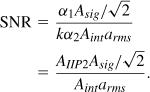
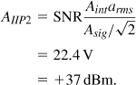
This study reveals the relatively high IP2 values required in direct-conversion receivers. We deal with methods of achieving a high IP2 in Chapter 6.
Flicker Noise
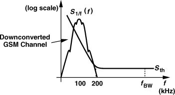
Since linearity requirements typically limit the gain of the LNA/mixer cascade to about 30 dB, the downconverted signal in a direct-conversion receiver is still relatively small and hence susceptible to noise in the baseband circuits. Furthermore, since the signal is centered around zero frequency, it can be substantially corrupted by flicker noise. As explained in Chapter 6, the mixers themselves may also generate flicker noise at their output.
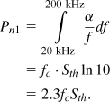
In order to quantify the effect of flicker noise, let us assume the downconverted spectrum shown in Fig. 4.44, where fBW is half of the RF channel bandwidth. The flicker noise is denoted by S1/f and the thermal noise at the end of the baseband by Sth. The frequency at which the two profiles meet is called fc. We wish to determine the penalty due to flicker noise, i.e., the additional noise power contributed by S1/f. To this end, we note that if S1/f = α/f, then at fc,
![]()
Figure 4.44 Spectrum for calculation of flicker noise.

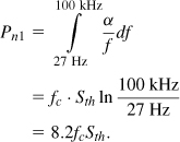
That is, α = fc · Sth. Also, we assume noise components below roughly fBW/1000 are unimportant because they vary so slowly that they negligibly affect the baseband symbols.16 The total noise power from fBW/1000 to fBW is equal to
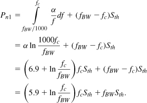
In the absence of flicker noise, the total noise power from fBW/1000 to fBW is given by
![]()
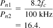
The ratio of Pn1 and Pn2 can serve as a measure of the flicker noise penalty:
![]()
How do the above results depend on the gain of the LNA/mixer cascade? In a good design, the thermal noise at the end of the baseband chain arises mostly from the noise of the antenna, the LNA, and the mixer. Thus, a higher front-end gain directly raises Sth in Fig. 4.44, thereby lowering the value of fc and hence the flicker noise penalty.
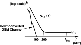
As evident from the above example, the problem of flicker noise makes it difficult to employ direct conversion for standards that have a narrow channel bandwidth. In such cases, the “low-IF” architecture proves a more viable choice (Section 4.2.5).
I/Q Mismatch
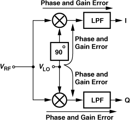
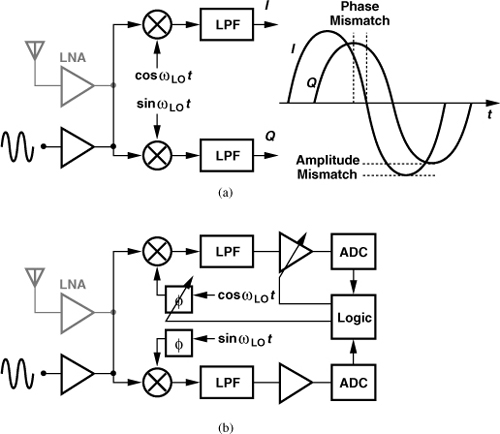
As explained in Section 4.2.2, downconversion of an asymmetrically-modulated signal to a zero IF requires separation into quadrature phases. This can be accomplished by shifting either the RF signal or the LO waveform by 90° (Fig. 4.46). Since shifting the RF signal generally entails severe noise-power-gain trade-offs, the approach in Fig. 4.46(b) is preferred. In either case, as illustrated in Fig. 4.47, errors in the 90° phase shift circuit and mismatches between the quadrature mixers result in imbalances in the amplitudes and phases of the baseband I and Q outputs. The baseband stages themselves may also contribute significant gain and phase mismatches.17
Figure 4.46 Shift of (a) RF signal, or (b) LO waveform by 90°.
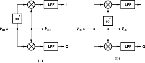
Figure 4.47 Sources of I and Q mismatch.
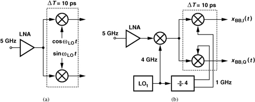
Quadrature mismatches tend to be larger in direct-conversion receivers than in heterodyne topologies. This occurs because (1) the propagation of a higher frequency (fin) through quadrature mixers experiences greater mismatches; for example, a delay mismatch of 10 ps between the two mixers translates to a phase mismatch of 18° at 5 GHz [Fig. 4.48(a)] and 3.6° at 1 GHz [Fig. 4.48(b)]; or (2) the quadrature phases of the LO itself suffer from greater mismatches at higher frequencies; for example, since device dimensions are reduced to achieve higher speeds, the mismatches between transistors increase.
Figure 4.48 Effect of a 10-ps propagation mismatch on a (a) direct-conversion and (b) heterodyne receiver.
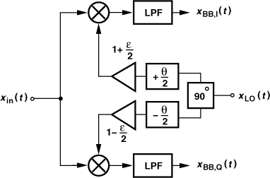
To gain insight into the effect of I/Q imbalance, consider a QPSK signal, xin(t) = a cos ωct + b sin ωct, where a and b are either −1 or +1. Now let us lump all of the gain and phase mismatches shown in Fig. 4.47 in the LO path (Fig. 4.49)
![]()
![]()
where the factor of 2 is included to simplify the results and ![]() and θ represent the amplitude and phase mismatches, respectively. Multiplying xin(t) by the quadrature LO waveforms and low-pass filtering the results, we obtain the following baseband signals:
and θ represent the amplitude and phase mismatches, respectively. Multiplying xin(t) by the quadrature LO waveforms and low-pass filtering the results, we obtain the following baseband signals:
![]()
![]()
Figure 4.49 Mismatches lumped in LO path.
We now examine the results for two special cases: ![]() ≠ 0, θ = 0 and
≠ 0, θ = 0 and ![]() = 0, θ ≠ 0. In the former case, xBB,I(t) = a(1 +
= 0, θ ≠ 0. In the former case, xBB,I(t) = a(1 + ![]() /2) and xBB,Q(t) = b(1 −
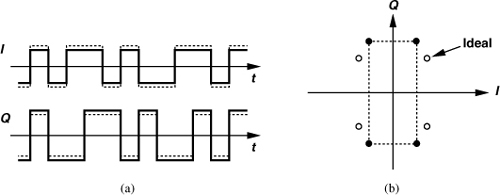
/2) and xBB,Q(t) = b(1 − ![]() /2), implying that the quadrature baseband symbols are scaled differently in amplitude [Fig. 4.50(a)]. More importantly, the points in the constellation are displaced [Fig. 4.50(b)].
/2), implying that the quadrature baseband symbols are scaled differently in amplitude [Fig. 4.50(a)]. More importantly, the points in the constellation are displaced [Fig. 4.50(b)].
Figure 4.50 Effect of gain mismatch on (a) time-domain waveforms and (b) constellation of a QPSK signal.
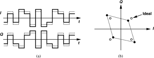
With ![]() = 0 θ ≠ 0, we have xBB,I(t) = a cos(θ/2) − b sin(θ/2) and xBB,Q(t) = −a sin(θ/2) + b cos(θ/2). That is, each baseband output is corrupted by a fraction of the data symbols in the other output [Fig. 4.51(a)]. Also, the constellation is compressed along one diagonal and stretched along the other [Fig. 4.51(b)].
= 0 θ ≠ 0, we have xBB,I(t) = a cos(θ/2) − b sin(θ/2) and xBB,Q(t) = −a sin(θ/2) + b cos(θ/2). That is, each baseband output is corrupted by a fraction of the data symbols in the other output [Fig. 4.51(a)]. Also, the constellation is compressed along one diagonal and stretched along the other [Fig. 4.51(b)].
Figure 4.51 Effect of phase mismatch on (a) time-domain waveforms and (b) constellation of a QPSK signal.
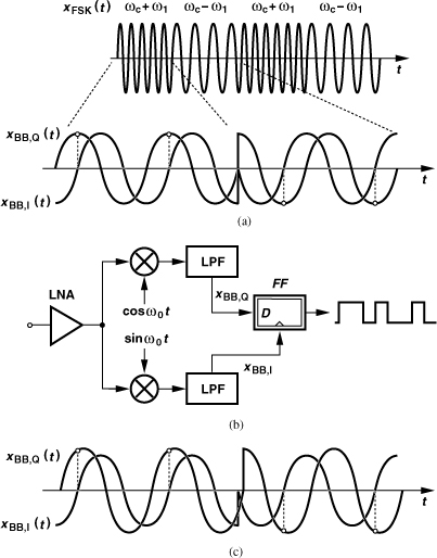
Solution:
![]()
![]()
Figure 4.52 (a) Baseband waveforms for an FSK signal, (b) FSK detection by a D flipflop, (c) effect of phase and gain mismatches.
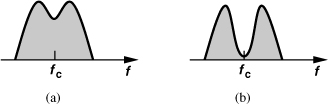
In the design of an RF receiver, the maximum tolerable I/Q mismatch must be known so that the architecture and the building blocks are chosen accordingly. For complex signal waveforms such as OFDM with QAM, this maximum can be obtained by simulations: the bit error rate is plotted for different combinations of gain and phase mismatches, providing the maximum mismatch values that affect the performance negligibly. (The EVM can also reflect the effect of these mismatches.) As an example, Fig. 4.53 plots the BER curves for a system employing OFDM with 128 subchannels and QPSK modulation in each subchannel [1]. We observe that gain/phase mismatches below −0.6 dB/6° have negligible effect.
Figure 4.53 Effect of I/Q mismatch on an OFDM signal with QPSK modulation. (![]() : no imbalance;°: θ = 6°,
: no imbalance;°: θ = 6°, ![]() = 0.6 dB;
= 0.6 dB; ![]() : θ = 10°,
: θ = 10°, ![]() = 0.8 dB; Δ: θ = 16°,
= 0.8 dB; Δ: θ = 16°, ![]() = 1.4 dB.)
= 1.4 dB.)

In standards such as 802.11a/g, the required phase and gain mismatches are so small that the “raw” matching of the devices and the layout may not suffice. Consequently, in many high-performance systems, the quadrature phase and gain must be calibrated—either at power-up or continuously. As illustrated in Fig. 4.54(a), calibration at power-up can be performed by applying an RF tone at the input of the quadrature mixers and observing the baseband sinusoids in the analog or digital domain [2]. Since these sinusoids can be produced at arbitrarily low frequencies, their amplitude and phase mismatches can be measured accurately. With the mismatches known, the received signal constellation is corrected before detection. Alternatively, as depicted in Fig. 4.54(b), a variable-phase stage, ϕ, and a variable-gain stage can be inserted in the LO and baseband paths, respectively, and adjusted until the mismatches are sufficiently small. Note that the adjustment controls must be stored digitally during the actual operation of the receiver.
Figure 4.54 (a) Computation and (b) correction of I/Q mismatch in a direct-conversion receiver.
Mixing Spurs
Unlike heterodyne systems, direct-conversion receivers rarely encounter corruption by mixing spurs. This is because, for an input frequency f1 to fall in the baseband after experiencing mixing with nfLO, we must have f1 ≈ nfLO. Since fLO is equal to the desired channel frequency, f1 lies far from the band of interest and is greatly suppressed by the selectivity of the antenna, the band-select filter, and the LNA.
The issue of LO harmonics does manifest itself if the receiver is designed for a wide frequency band (greater than two octaves). Examples include TV tuners, “software-defined radios,” and “cognitive radios.”
4.2.4 Image-Reject Receivers
Our study of heterodyne and direct-conversion receivers has revealed various pros and cons. For example, heterodyning must deal with the image and mixing spurs and direct conversion, with even-order distortion and flicker noise. “Image-reject” architectures are another class of receivers that suppress the image without filtering, thereby avoiding the trade-off between image rejection and channel selection.
90° Phase Shift
Before studying these architectures, we must define a “shift-by-90°” operation. First, let us consider a tone, A cos ωct = (A/2)[exp(+jωct) + exp(−jωct)]. The two exponentials respectively correspond to impulses at +ωc and −ωc in the frequency domain. We now shift the waveform by 90°:

Equivalently, the impulse at +ωc is multiplied by −j and that at −ωc, by +j. We illustrate this transformation in the three-dimensional diagram of Fig. 4.55(a), recognizing that the impulse at +ωc is rotated clockwise and that at −ωc counterclockwise.
Figure 4.55 Illustration of 90° phase shift for (a) a cosine and (b) a modulated signal.

Similarly, for a narrowband modulated signal, x(t) = A(t) cos [ωct + φ(t)], we perform a 90° phase shift as
As depicted in Fig. 4.55(b), the positive-frequency contents are multiplied by −j and the negative-frequency contents by +j (if ωc is positive). Alternatively, we write in the frequency domain:
![]()
where sgn (ω) denotes the signum (sign) function. The shift-by-90° operation is also called the “Hilbert transform.” The reader can prove that the Hilbert transform of the Hilbert transform (i.e., the cascade of two 90° phase shifts) simply negates the original signal.
The Hilbert transform, as expressed by Eq. (4.67), distinguishes between negative and positive frequencies. This distinction is the key to image rejection.
Solution:
Figure 4.56 (a) A sine subjected to 90° phase shift, (b) spectrum of A cos ωct + j sin ωct.
Solution:
Figure 4.57 (a) 90° phase shift applied to I to produce Q, (b) multiplication of the result by j, (c) analytic signal.

How is the 90° phase shift implemented? Consider the RC-CR network shown in Fig. 4.58(a), where the high-pass and low-pass transfer functions are respectively given by
![]()
![]()
Figure 4.58 (a) Use of an RC-CR network to perform a 90° phase shift, (b) frequency response of the network.
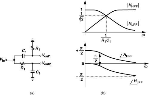
The transfer functions exhibit a phase of ∠HHPF = π/2 − tan−1(R1C1ω) and ∠HLPF = −tan−1(R1C1ω). Thus, ∠HHPF − ∠HLPF = π/2 at all frequencies and any choice of R1 and C1. Also, ![]() [Fig. 4.58(b)]. We can therefore consider Vout2 as the Hilbert transform of Vout1 at frequencies close to (R1C1)−1.
[Fig. 4.58(b)]. We can therefore consider Vout2 as the Hilbert transform of Vout1 at frequencies close to (R1C1)−1.
Another approach to realizing the 90°-phase-shift operation is illustrated in Fig. 4.59(a), where the RF input is mixed with the quadrature phases of the LO so as to translate the spectrum to a nonzero IF. As shown in Fig. 4.59(b), as a result of mixing with cos ωLOt, the impulse at −ωLO is convolved with the input spectrum around +ωc, generating that at −ωIF. Similarly, the impulse at +ωLO produces the spectrum at +ωIF from that at −ωc. Depicted in Fig. 4.59(c), mixing with sin ωLOt results in an IF spectrum at −ωIF with a coefficient +j/2 and another at +ωIF with a coefficient −j/2. We observe that, indeed, the IF spectrum emerging from the lower arm is the Hilbert transform of that from the upper arm.
Figure 4.59 (a) Quadrature downconversion as a 90° phase shifter, (b) output spectrum resulting from multiplication by cos ωLOt, (c) output spectrum resulting from multiplication by sin ωLOt.
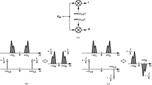
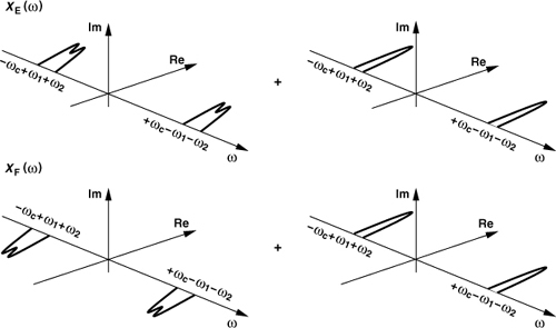
Let us summarize our findings thus far. The quadrature converter19 of Fig. 4.59(a) produces at its output a signal and its Hilbert transform if ωc > ωLO or a signal and the negative of its Hilbert transform if ωc < ωLO. This arrangement therefore distinguishes between the desired signal and its image. Figure 4.61 depicts the three-dimensional IF spectra if a signal and its image are applied at the input and ωLO < ωc.
Figure 4.61 Input and output spectra in a quadrature downconverter with low-side injection.
Hartley Architecture
How can the image components in Fig. 4.61 cancel each other? For example, is I(t) + Q(t) free from the image? Since the image components in Q(t) are 90° out of phase with respect to those in I(t), this summation still contains the image. However, since the Hilbert transform of the Hilbert transform negates the signal, if we shift I(t) or Q(t) by another 90° before adding them, the image may be removed. This hypothesis forms the foundation for the Hartley architecture shown in Fig. 4.62. (The original idea proposed by Hartley relates to single-sideband transmitters [4].) The low-pass filters are inserted to remove the unwanted high-frequency components generated by the mixers.
Figure 4.62 Hartley image-reject receiver.
To understand the operation of Hartley’s architecture, we assume low-side injection and apply a 90° phase shift to the Hilbert transforms of the signal and the image (the Q arm) in Fig. 4.61, obtaining Qsig,90° and Qim,90° as shown in Fig. 4.63. Multiplication of Qsig by −jsgn(ω) rotates and superimposes the spectrum of Qsig on that of Isig (from Fig. 4.61), doubling the signal amplitude. On the other hand, multiplication of Qim by −jsgn(ω) creates the opposite of Iim, cancelling the image.
Figure 4.63 Spectra at points B and C in Hartley receiver.

In summary, the Hartley architecture first takes the negative Hilbert transform of the signal and the Hilbert transform of the image (or vice versa) by means of quadrature mixing, subsequently takes the Hilbert transform of one of the downconverted outputs, and sums the results. That is, the signal spectrum is multiplied by [+jsgn(ω)][−jsgn(ω)] = +1, whereas the image spectrum is multiplied by [−jsgn(ω)][−jsgn(ω)] = −1.
The behavior of the Hartley architecture can also be expressed analytically. Let us represent the received signal and image as x(t) = Asig cos(ωct + ϕsig) + Aim cos(ωimt + ϕim), where the amplitudes and phases are functions of time in the general case. Multiplying x(t) by the LO phases and neglecting the high-frequency components, we obtain the signals at points A and B in Fig. 4.62:
![]()
![]()
where a unity LO amplitude is assumed for simplicity. Now, xB(t) must be shifted by 90°. With low-side injection, the first sine has a positive frequency and becomes negative of a cosine after the 90° shift (why?). The second sine, on the other hand, has a negative frequency. We therefore write −(Aim/2) sin[(ωim − ωLO)t + ϕim] = (Aim/2) sin[(ωLO − ωim)t − ϕim] so as to obtain a positive frequency and shift the result by 90°, arriving at −(Aim/2) cos[(ωLO − ωim)t − ϕim] = −(Aim/2) cos[(ωim − ωLO)t + ϕim]. It follows that
![]()
Upon addition of xA(t) and xC(t), we retain the signal and reject the image.
The 90° phase shift depicted in Fig. 4.62 is typically realized as a +45° shift in one path and −45° shift in the other (Fig. 4.64). This is because it is difficult to shift a single signal by 90° while circuit components vary with process and temperature.
Figure 4.64 Realization of 90° phase shift in Hartley receiver.

The principal drawback of the Hartley architecture stems from its sensitivity to mismatches: the perfect image cancellation described above occurs only if the amplitude and phase of the negative of the image exactly match those of the image itself. If the LO phases are not in exact quadrature or the gains and phase shifts of the upper and lower arms in Fig. 4.64 are not identical, then a fraction of the image remains. To quantify this effect, we lump the mismatches of the receiver as a single amplitude error, ![]() , and phase error, Δθ, in the LO path, i.e., one LO waveform is expressed as sin ωLOt and the other as (1 +
, and phase error, Δθ, in the LO path, i.e., one LO waveform is expressed as sin ωLOt and the other as (1 + ![]() ) cos(ωLOt + Δθ). Expressing the received signal and image as x(t) = Asig cos(ωct + ϕsig) + Aim cos(ωimt + ϕim) and multiplying x(t) by the LO waveforms, we write the downconverted signal at point A in Fig. 4.62 as
) cos(ωLOt + Δθ). Expressing the received signal and image as x(t) = Asig cos(ωct + ϕsig) + Aim cos(ωimt + ϕim) and multiplying x(t) by the LO waveforms, we write the downconverted signal at point A in Fig. 4.62 as
The spectra at points B and C are still given by Eqs. (4.71) and (4.72), respectively. We now add xA(t) and xC(t) and group the signal and image components at the output:
To arrive at a meaningful measure of the image rejection, we divide the image-to-signal ratio at the input by the same ratio at the output.20 The result is called the “image rejection ratio” (IRR). Noting that the average power of the vector sum a cos(ωt + α) + b cos ωt is given by (a2 + 2ab cos α + b2)/2, we write the output image-to-signal ratio as
![]()
Since the image-to-signal ratio at the input is given by ![]() , the IRR can be expressed as
, the IRR can be expressed as
![]()
Note that ![]() denotes the relative gain error and Δθ is in radians. Also, to express IRR in dB, we must compute 10 log IRR (rather than 20 log IRR).
denotes the relative gain error and Δθ is in radians. Also, to express IRR in dB, we must compute 10 log IRR (rather than 20 log IRR).
If ![]()
![]() 1 rad, simplify the expression for IRR.
1 rad, simplify the expression for IRR.
Solution:
Since cos Δθ ≈ 1 − Δθ2/2 for Δθ ![]() 1 rad, we can reduce (4.77) to
1 rad, we can reduce (4.77) to
![]()
In the numerator, the first term dominates and in the denominator ![]()
![]() 1, yielding
1, yielding
![]()
For example, ![]() = 10% (≈ 0.83 dB)21 limits the IRR to 26 dB. Similarly, Δθ = 10° yields an IRR of 21 dB. While such mismatch values may be tolerable in direct-conversion receivers, they prove inadequate here.
= 10% (≈ 0.83 dB)21 limits the IRR to 26 dB. Similarly, Δθ = 10° yields an IRR of 21 dB. While such mismatch values may be tolerable in direct-conversion receivers, they prove inadequate here.
With various mismatches arising in the LO and signal paths, the IRR typically falls below roughly 35 dB. This issue and a number of other drawbacks limit the utility of the Hartley architecture.
Another critical drawback, especially in CMOS technology, originates from the variation of the absolute values of R1 and C1 in Fig. 4.64. Recall from Fig. 4.58 that the phase shift produced by the RC-CR network remains equal to 90° even with such variations, but the output amplitudes are equal at only ω = (R1C1)−1. Specifically, if R1 and C1 are nominally chosen for a certain IF, (R1C1)−1 = ωIF, but respectively experience a small change of ΔR and ΔC with process or temperature, then the ratio of the output amplitudes of the high-pass and low-pass sections is given by

Thus, the gain mismatch is equal to
![]()
For example, ΔR/R1 = 20% limits the image rejection to only 20 dB. Note that these calculations have assumed perfect matching between the high-pass and low-pass sections. If the resistors or capacitors exhibit mismatches, the IRR degrades further.
Another drawback resulting from the RC-CR sections manifests itself if the signal translated to the IF has a wide bandwidth. Since the gains of the high-pass and low-pass sections depart from each other as the frequency departs from ωIF = (R1C1)−1 [Fig. 4.58(b)], the image rejection may degrade substantially near the edges of the channel. In Problem 4.17, the reader can prove that, at a frequency of ωIF + Δω, the IRR is given by
![]()
For example, a fractional bandwidth of 2Δω/ωIF = 5% limits the IRR to 32 dB.
The limitation expressed by Eq. (4.83) implies that ωIF cannot be zero, dictating a heterodyne approach. Figure 4.65 shows an example where the first IF is followed by another quadrature downconverter so as to produce the baseband signals. Unlike the sliding-IF architecture of Fig. 4.26(a), this topology also requires the quadrature phases of the first LO, a critical disadvantage. The mixing spurs studied in Section 4.2.1 persist here as well.
Figure 4.65 Downconversion of Hartley receiver output to baseband.
The RC-CR sections used in Fig. 4.64 also introduce attenuation and noise. The 3-dB loss resulting from ![]() at ω = (R1C1)−1 directly amplifies the noise of the following adder. Moreover, the input impedance of each section, |R1 + (C1s)−1 |, reaches
at ω = (R1C1)−1 directly amplifies the noise of the following adder. Moreover, the input impedance of each section, |R1 + (C1s)−1 |, reaches ![]() at ω = (R1C1)−1, imposing a trade-off between the loading seen by the mixers and the thermal noise of the 90° shift circuit.
at ω = (R1C1)−1, imposing a trade-off between the loading seen by the mixers and the thermal noise of the 90° shift circuit.
The voltage adder at the output of the Hartley architecture also poses difficulties as its noise and nonlinearity appear in the signal path. Illustrated in Fig. 4.66, the summation is typically realized by differential pairs, which convert the signal voltages to currents, sum the currents, and convert the result to a voltage.
Figure 4.66 Summation of two voltages.

Weaver Architecture
Our analysis of the Hartley architecture has revealed several issues that arise from the use of the RC-CR phase shift network. The Weaver receiver, derived from its transmitter counterpart [5], avoids these issues.
As recognized in Fig. 4.59, mixing a signal with quadrature phases of an LO takes the Hilbert transform. Depicted in Fig. 4.67, the Weaver architecture replaces the 90° phase shift network with quadrature mixing. To formulate the circuit’s behavior, we begin with xA(t) and xB(t) as given by Eqs. (4.70) and (4.71), respectively, and perform the second quadrature mixing operation, arriving at
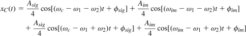
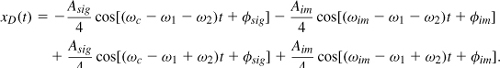
Figure 4.67 Weaver architecture.
Should these results be added or subtracted? Let us assume low-side injection for both mixing stages. Thus, ωim < ω1 and ω1 − ωim > ω2 (Fig. 4.68). Also, ω1 − ωim + ω2 > ω1 − ωim −ω2. The low-pass filters following points C and D in Fig. 4.67 must therefore remove the components at ω1 − ωim + ω2 (= ωc − ω1 + ω2), leaving only those at ω1 − ωim − ω2 (= ωc − ω1 − ω2). That is, the second and third terms in Eqs. (4.84) and (4.85) are filtered. Upon subtracting xF(t) from xE(t), we obtain
![]()
Figure 4.68 RF and IF spectra in Weaver architecture.

The image is therefore removed. In Problem 4.19, we consider the other three combinations of low-side and high-side injection so as to determine whether the outputs must be added or subtracted.
While employing two more mixers and one more LO than the Hartley architecture, the Weaver topology avoids the issues related to RC-CR networks: resistance and capacitance variations, degradation of IRR as the frequency departs from 1/(R1C1), attenuation, and noise. Also, if the IF mixers are realized in active form (Chapter 6), their outputs are available in the current domain and can be summed directly. Nonetheless, the IRR is still limited by mismatches, typically falling below 40 dB.
The Weaver architecture must deal with a secondary image if the second IF is not zero. Illustrated in Fig. 4.70, this effect arises if a component at 2ω2 −ωin + 2ω1 accompanies the RF signal. Downconversion to the first IF translates this component to 2ω2 − ωin + ω1, i.e., image of the signal with respect to ω2, and mixing with ω2 brings it to ω2 − ωin + ω1, the same IF at which the signal appears. For this reason, the second downconversion preferably produces a zero IF, in which case it must perform quadrature separation as well. Figure 4.71 shows an example [6], where the second LO is derived from the first by frequency division.
Figure 4.70 Secondary image in Weaver architecture.

Figure 4.71 Double quadrature downconversion Weaver architecture to produce baseband outputs.
The Weaver topology also suffers from mixing spurs in both downconversion steps. In particular, the harmonics of the second LO frequency may downconvert interferers from the first IF to baseband.
Calibration
For image-rejection ratios well above 40 dB, the Hartley or Weaver architectures must incorporate calibration, i.e., a method of cancelling the gain and phase mismatches. A number of calibration techniques have been reported [7, 9].
4.2.5 Low-IF Receivers
In our study of heterodyne receivers, we noted that it is undesirable to place the image within the signal band because the image thermal noise of the antenna, the LNA, and the input stage of the RF mixer would raise the overall noise figure by approximately 3 dB.22 In “low-IF receivers,” the image indeed falls in the band but is suppressed by image rejection operations similar to those described in Section 4.2.4. To understand the motivation for the use of low-IF architectures, let us consider a GSM receiver as an example. As explained in Section 4.2.3, direct conversion of the 200-kHz desired channel to a zero IF may significantly corrupt the signal by 1/f noise. Furthermore, the removal of the dc offset by means of a high-pass filter proves difficult. Now suppose the LO frequency is placed at the edge of the desired (200-kHz) channel [Fig. 4.72(a)], thereby translating the RF signal to an IF of 100 kHz. With such an IF, and because the signal carries little information near the edge, the 1/f noise penalty is much less severe. Also, on-chip high-pass filtering of the signal becomes feasible. Called a “low-IF receiver,” this type of system is particularly attractive for narrow-channel standards.
Figure 4.72 (a) Spectra in a low-IF receiver, (b) adjacent-channel specification in GSM.
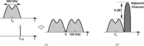
The heterodyne downconversion nonetheless raises the issue of the image, which in this case falls in the adjacent channel. Fortunately, the GSM standard requires that receivers tolerate an adjacent channel only 9 dB above the desired channel (Chapter 3) [Fig. 4.72(b)]. Thus, an image-reject receiver with a moderate IRR can lower the image to well below the signal level. For example, if IRR = 30 dB, the image remains 21 dB below the signal.
How is image rejection realized in a low-IF receiver? The Hartley architecture employing the RC-CR network (Fig. 4.64) appears to be a candidate, but the IF spectrum in a low-IF RX may extend to zero frequency, making it impossible to maintain a high IRR across the signal bandwidth. (The high-pass Section exhibits zero gain near frequency!) While avoiding this issue, the Weaver architecture must deal with the secondary image if the second IF is not zero or with flicker noise if it is.
One possible remedy is to move the 90° phase shift in the Hartley architecture from the IF path to the RF path. Illustrated in Fig. 4.74, the idea is to first create the quadrature phases of the RF signal and the image and subsequently perform another Hilbert transform by means of quadrature mixing. We also recognize some similarity between this topology and the Weaver architecture: both multiply quadrature components of the signal and the image by the quadrature phases of the LO and sum the results, possibly in the current domain. Here, the RC-CR network is centered at a high frequency and can maintain a reasonable IRR across the band. For example, for the 25-MHz receive band of 900-MHz GSM, if (2πR1C1)−1 is chosen equal to the center frequency, then Eq. (4.83) implies an IRR of 20 log(900 MHz/12.5 MHz) = 37 dB. However, the variation of R1 and C1 still limits the IRR to about 20 dB [Eq. (4.82)].
Figure 4.74 Quadrature phase separation in RF path of a Hartley receiver.
Another variant of the low-IF architecture is shown in Fig. 4.75. Here, the downconverted signals are applied to channel-select filters and amplifiers as in a direct-conversion receiver.23 The results are then digitized and subjected to a Hilbert transform in the digital domain before summation. Avoiding the issues related to the analog 90° phase shift operation, this approach proves a viable choice. Note that the ADCs must accommodate a signal bandwidth twice that in a direct-conversion receiver, thus consuming higher power. This issue is unimportant in narrow-channel standards such as GSM because the ADC power dissipation is but a small fraction of that of the overall system.
Figure 4.75 Low-IF receiver with 90° phase shift in digital domain.
Let us summarize our thoughts thus far. If a low-IF receiver places the image in the adjacent channel, then it cannot employ an RC-CR 90° phase shift after downconversion. Also, a 90° circuit in the RF path still suffers from RC variation. For these reasons, the concept of “low IF” can be extended to any downconversion that places the image within the band so that the IF is significantly higher than the signal bandwidth, possibly allowing the use of an RC-CR network—but not so high as to unduly burden the ADC. Of course, since the image no longer lies in the adjacent channel, a substantially higher IRR may be required. Some research has therefore been expended on low-IF receivers with high image rejection. Such receivers often employ “polyphase filters” (PPFs) [10, 11].
Polyphase Filters
Recall from Section 4.2.4 that heterodyne quadrature downconversion subjects the signal to low-side injection and the image to high-side injection, or vice versa, thus creating the Hilbert transform of one and the negative Hilbert transform of the other. Now let us consider the circuit shown in Fig. 4.76(a), where Vout can be viewed as a weighted sum of V1 and V2:
![]()
Figure 4.76 (a) Simple RC circuit, (b) output in response to V1 and −jV1, (c) output in response to V1 and +jV1.
We consider two special cases.
1. The voltage V2 is the Hilbert transform of V1; in phasor form, V2 = −jV1 (Example 4.26). Consequently, for s = jω,
![]()
If ω = (R1C1)−1, then Vout = 2V1/(1 + j) = V1(1 − j). That is, ![]() and ∠Vout = ∠Vin − 45° [Fig. 4.76(b)]. In this case, the circuit simply computes the vector summation of V1 and V2 = −jV1. We say the circuit rotates by −45° the voltage sensed by the resistor.
and ∠Vout = ∠Vin − 45° [Fig. 4.76(b)]. In this case, the circuit simply computes the vector summation of V1 and V2 = −jV1. We say the circuit rotates by −45° the voltage sensed by the resistor.
2. The voltage V2 is the negative Hilbert transform of V1, i.e., V2 = +jV1. For s = jω,
![]()
Interestingly, if ω = (R1C1)−1, then Vout = 0 [Fig. 4.76(c)]. Intuitively, we can say that C1 rotates V2 by another 90° so that the result cancels the effect of V1 at the output node. The reader is encouraged to arrive at these conclusions using superposition.
In summary, the series branch of Fig. 4.76(a) rotates V1 by −45° (to produce Vout) if V2 = −jV1 and rejects V1 if V2 = +jV1. The circuit can therefore distinguish between the signal and the image if it follows a quadrature downconverter.
Solution:
Figure 4.77 (a) RC circuit sensing differential inputs, (b) quadrature downconverter driving RC network of part (a).
In contrast to the Hartley architecture of Fig. 4.62, the circuit of Fig. 4.77(b) avoids an explicit voltage adder at the output. Nonetheless, this arrangement still suffers from RC variations and a narrow bandwidth. In fact, at an IF of ω = (R1C1)−1 + Δω, Eq. (4.94) yields the residual image as
where it is assumed that Δω ![]() ω.
ω.
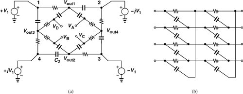
In the next step of our development of polyphase filters, let us now redraw the circuit of Fig. 4.77(a) and add two branches to it as shown in Fig. 4.78(a). Here, the capacitors are equal and so are the resistors. The top and bottom branches still produce differential outputs, but how about the left and right branches? Since R3 and C3 compute the weighted sum of +jV1 and +V1, we observe from Fig. 4.76(b) that Vout3 is 45° more negative than +jV1. By the same token, Vout4 is 45° more negative than −jV1. Figure 4.78(b) depicts the resulting phasors at ω = (R1C1)−1, suggesting that the circuit produces quadrature outputs that are 45° out of phase with respect to the quadrature inputs.
Figure 4.78 (a) RC network sensing differential quadrature phases, (b) resulting outputs.
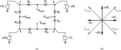
Figure 4.79 (a) Quadrature downconverter driving RC sections, (b) resulting signal output, (c) resulting image output.

Solution:
The multiphase circuit of Fig. 4.78(a) is called a “sequence-asymmetric polyphase filter” [8]. Since the signal and the image arrive at the inputs with different sequences, one is passed to the outputs while the other is suppressed. But what happens if ω ≠ (RC)−1? Substituting ω = (R1C1)−1 + Δω in Eq. (4.93), we have
![]()
and hence,
That is,
![]()
The phase of Vout1 is obtained from (4.97) as
![]()
Since tan−1(1 + RC Δω) ≈ π/4 + RC Δω/2 for RC Δω ![]() 1 rad,
1 rad,
![]()
Figure 4.80(a) illustrates the effect on all four phases of the signal, implying that the outputs retain their differential and quadrature relationship.
Figure 4.80 Effect of polyphase filter at a frequency offset of Δω for (a) signal, and (b) image.
For the image, we return to Eq. (4.96) and note that the four outputs have a magnitude equal to ![]() and phases similar to those of the signal components in Fig. 4.80(a). The output image phasors thus appear as shown in Fig. 4.80(b). The reader is encouraged to prove that Vout1 is at −45° − RCΔω/2 and Vout3 at −135° − RC Δω/2.
and phases similar to those of the signal components in Fig. 4.80(a). The output image phasors thus appear as shown in Fig. 4.80(b). The reader is encouraged to prove that Vout1 is at −45° − RCΔω/2 and Vout3 at −135° − RC Δω/2.
An interesting observation in Fig. 4.80 is that the output signal and image components exhibit opposite sequences [10, 11]. We therefore expect that if this polyphase filter is followed by another, then the image can be further suppressed. Figure 4.81(a) depicts such a cascade and Fig. 4.81(b) shows an alternative drawing that more easily lends itself to cascading.
Figure 4.81 (a) Cascaded polyphase sections, (b) alternative drawing.
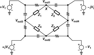
We must now answer two questions: (1) how should we account for the loading of the second stage on the first? (2) how are the RC values chosen in the two stages? To answer the first question, consider the equivalent circuit shown in Fig. 4.82, where Z1-Z4 represent the RC branches in the second stage. Intuitively, we note that Z1 attempts to “pull” the phasors Vout1 and Vout3 toward each other, Z2 attempts to pull Vout1 and Vout4 toward each other, etc. Thus, if Z1 = ... = Z4 = Z, then, Vout1–Vout4 experience no rotation, but the loading may reduce their magnitudes. Since the angles of Vout1–Vout4 remain unchanged, we can express them as ±α(1 ± j)V1, where α denotes the attenuation due to the loading of the second stage. The currents drawn from node X by Z1 and Z2 are therefore equal to [α(1 − j)V1 − α(1 + j)V1]/Z1 and [α(1 − j)V1 + α(1 + j)V1]/Z2, respectively. Summing all of the currents flowing out of node X and equating the result to zero, we have

Figure 4.82 Effect of loading of second polyphase section.
This equality must hold for any nonzero value of V1. If RCω = 1, the expression reduces to
![]()
That is,
![]()
For example, if Z = R + (jCω)−1, then α = 1/2, revealing that loading by an identical stage attenuates the outputs of the first stage by a factor of 2.
Solution:
![]()
In comparison with Fig. 4.76(b), we note that a two-section polyphase filter produces an output whose magnitude is ![]() times smaller than that of a single-section counterpart. We say each section attenuates the signal by a factor of
times smaller than that of a single-section counterpart. We say each section attenuates the signal by a factor of ![]() .
.
The second question relates to the choice of RC values. Suppose both stages employ RC = R0C0. Then, the cascade of two stages yields an image attenuation equal to the square of Eq. (4.95) at a frequency of (R0C0)−1 + Δω:
![]()
which reduces to (R0C0 Δω)2/2 for Δω ![]() (R0C0)−1. Figure 4.83 plots this behavior, comparing it with that of a single section.
(R0C0)−1. Figure 4.83 plots this behavior, comparing it with that of a single section.
Figure 4.83 Image rejection for single-stage and two-stage polyphase filters.
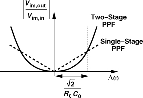
What happens if the two stages use different time constants? In particular, for a given IF of ω0, let us assume that the time constants in the first and second stages are respectively equal to R1C1 and R2C2 such that ω0 − (R1C1)−1 = (R2C2)−1 − ω0, i.e., the center frequencies are shifted up and down. From Eq. (4.96), we plot the image rejections of the two stages as shown in Fig. 4.84(a).24 The product of these two functions is a parabola crossing zero at ω1 = (R1C1)−1 and ω2 = (R2C2)−1 [Fig. 4.84(b)]. The reader can prove that the attenuation at ω0 is equal to (ω1 − ω2)2/(8ω1ω2), which must be chosen sufficiently small. The reader can also show that for an attenuation of 60 dB, ω1 − ω2 cannot exceed approximately 18% of ω0.
Figure 4.84 (a) Image rejections of two unidentical polyphase stages, (b) cascade image rejection, (c) magnitude of cascade image rejection.
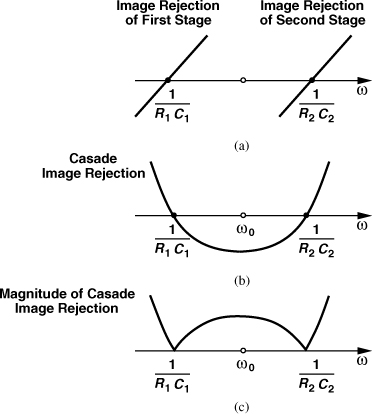
The advantage of splitting the cut-off frequencies of the two stages is the wider achievable bandwidth. Figure 4.85 plots the image rejection for ω1 = ω2 = ω0 and ω1 ≠ ω2.
Figure 4.85 Comparison of image rejections of two identical and unidentical polyphase stages.

The cascading of polyphase filter sections entails both attenuation and additional thermal noise. To alleviate the former, the resistors in the latter stages can be chosen larger than those in the former, but at the cost of higher noise. For this reason, polyphase filters are only occasionally used in RF receivers. In low-IF architectures, the polyphase filters can be realized as “complex filters” so as to perform channel-selection filtering [12].
Double-Quadrature Downconversion
In our study of the Hartley architecture, we noted that mismatches arise in both the RF signal path and the LO path. A method of reducing the effect of mismatches incorporates “double-quadrature” downconversion [10]. Illustrated in Fig. 4.86, the circuit decomposes the RF signal into quadrature components, performs quadrature downconversion on each of the RF components, and subtracts and adds the results to produce net quadrature IF outputs. It can be shown [10] that the overall gain and phase mismatches of this topology are given by

where ΔARF/ARF and ΔALO/ALO denote amplitude mismatches in the RF and LO paths, respectively, and ΔϕRF and ΔϕLO are the corresponding phase mismatches. The quantities ΔGmix/Gmix and Δϕmix denote the conversion gain mismatch and phase mismatch of the mixers, respectively. Thus, the IRR is only limited by mixer mismatches because the first terms on the right-hand sides of (4.109) and (4.110) are very small.
Figure 4.86 Low-IF receiver with double quadrature downconverter.

Equations (4.109) and (4.110) reveal that the IRR of the double-quadrature architecture is likely to fall well below 60 dB. This is because, even with no phase mismatch, ΔGmix/Gmix must remain less than 0.1% for IRR = 60 dB, a very stringent requirement even for matching of simple resistors. Calibration of the mismatches can therefore raise the IRR more robustly [7, 9].
4.3 Transmitter Architectures
4.3.1 General Considerations
An RF transmitter performs modulation, upconversion, and power amplification. In most of today’s systems, the data to be transmitted is provided in the form of quadrature baseband signals. For example, from Chapter 3 the GMSK waveform in GSM can be expanded as
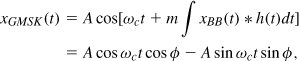
where
![]()
Thus, cos ϕ and sin ϕ are produced from xBB(t) by the digital baseband processor, converted to analog form by D/A converters, and applied to the transmitter.
We have seen the need for baseband pulse shaping in Chapter 3 and in the above equations for GMSK: each rectangular data pulse must be transformed to a smoother pulse. Since pulse shaping in the analog domain, especially at low frequencies, requires bulky filters, each incoming pulse is mapped to the desired shape by a combination of digital and analog techniques. Illustrated in Fig. 4.87 is an example [13, 14], where the input pulse generates a sequence of addresses, e.g., it enables a counter, producing a set of levels from two read-only memories (ROMs). (We say the pulse is “oversampled.”) These levels are subsequently converted to analog form, yielding the desired pulse shape at points A and B.
Figure 4.87 Baseband pulse shaping.

4.3.2 Direct-Conversion Transmitters
Most transmitter architectures are similar to the receiver topologies described in Section 4.2, but with the operations performed in “reverse” order. For example, an RX cascade of an LNA and quadrature downconversion mixers suggests a TX cascade of quadrature upconversion mixers and a PA.
The above expression of a GMSK waveform can be generalized to any narrowband modulated signal:
![]()
We therefore define the quadrature baseband signals as
![]()
![]()
and construct the transmitter as shown in Fig. 4.88. Called a “direct-conversion” transmitter, this topology directly translates the baseband spectrum to the RF carrier by means of a “quadrature upconverter.”25 The upconverter is followed by a PA and a matching network, whose role is to provide maximum power delivery to the antenna and filter out-of-band components that result from the PA nonlinearity (Chapter 12). Note that since the baseband signal is produced in the transmitter and hence has a sufficiently large amplitude (several hundred millivolts), the noise of the mixers is much less critical here than in receivers.
Figure 4.88 Direct-conversion transmitter.

The design of the TX begins with the PA. This circuit is crafted so as to deliver the required power to the antenna (and with adequate linearity if applicable). Employing large transistors to carry high currents, the PA exhibits a large input capacitance. Thus, a predriver is typically interposed between the upconverter and the PA to serve as a buffer.

Among various TX architectures studied in this chapter, the direct-conversion approach provides the most compact solution and a relatively “clean” output. That is, the output spectrum contains only the desired signal around the carrier frequency (and its harmonics) but no spurious components—an attribute similar to that of direct-conversion receivers. Nonetheless, direct upconversion entails other issues that demand attention.
I/Q Mismatch
We noted in Section 4.2 that I/Q mismatch in direct-conversion receivers results in “cross-talk” between the quadrature baseband outputs or, equivalently, distortion in the constellation. We expect a similar effect in the TX counterpart. For example, as derived in Chapter 3, a phase mismatch of Δθ in the upconverter shifts the constellation points of a QPSK signal to I = ± cos Δθ and Q = ±1 ± sin Δθ, just as observed for a direct-conversion receiver. The results obtained in Chapter 3 can be extended to include amplitude mismatch by writing
![]()
Since α1 and α2 assume ±1 values, the normalized coefficients of cos ωct and sin ωct appear as follows for the four points in the constellation:
![]()
![]()
![]()
![]()
The reader is encouraged to compute the error vector magnitude (Chapter 3) of this constellation.
Another approach to quantifying the I/Q mismatch in a transmitter involves applying two tones V0 cos ωint and V0 sin ωint to the I and Q inputs in Fig. 4.88 and examining the output spectrum. In the ideal case, the output is simply given by Vout = V0 cos ωint cos ωc t− V0 sin ωint sin ωct = V0 cos(ωc + ωin)t. On the other hand, in the presence of a (relative) gain mismatch of ε and a phase imbalance of Δθ, we have
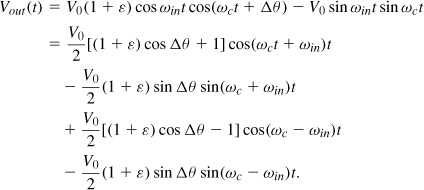
It follows that the power of the unwanted sideband at ωc −ωin divided by that of the wanted sideband at ωc + ωin is given by
which is similar to the image-rejection ratio expression [Eq. (4.77)]. We may even call the unwanted sideband the “image” of the wanted sideband with respect to the carrier frequency. In practice, a P−/P+ of roughly −30 dB is sufficient to ensure negligible distortion of the cancellation, but the exact requirement depends on the type of modulation.
If the raw I/Q matching of circuits in a transmitter is inadequate, some means of calibration can be employed. To this end, the gain and phase mismatch must first be measured and subsequently corrected. Can we use the power of the unwanted sideband as a symptom of the I/Q mismatch? Yes, but it is difficult to measure this power in the presence of the large wanted sideband: the two sidebands are too close to each other to allow suppressing the larger one by tens of decibels by means of a filter.
Let us now apply a single sinusoid to both inputs of the upconverter (Fig. 4.90). The output emerges as

Figure 4.90 Quadrature upconverter sensing a single sinusoid to reveal phase mismatch.
It can be shown that the output contains two sidebands of equal amplitudes and carries an average power equal to
![]()
We observe that ε is forced to zero as described above, then
![]()
Thus, the calibration of phase mismatch proceeds to drive this quantity to zero.
For gain mismatch calibration, we perform two consecutive tests. Depicted in Fig. 4.91, the tests entail applying a sinusoid to one baseband input while the other is set to zero. For the case in Fig. 4.91(a),
![]()
yielding an average power of
![]()
Figure 4.91 Quadrature upconverter sensing a cosine at (a) the I input, (b) at the Q input.
In Fig. 4.91(b), on the other hand,
![]()
producing
![]()
![]()
suggesting that the gain mismatch can be adjusted so as to drive this difference to zero.
The measurement of ![]() and
and ![]() in the above tests requires a relatively high resolution. For example, a residual phase mismatch of Δθ = 1° translates to sin Δθ = 1.75%, dictating a resolution of about 7–8 bits in the ADC that digitizes
in the above tests requires a relatively high resolution. For example, a residual phase mismatch of Δθ = 1° translates to sin Δθ = 1.75%, dictating a resolution of about 7–8 bits in the ADC that digitizes ![]() in Eq. (4.131).
in Eq. (4.131).
We should remark that dc offsets in the baseband may affect the accuracy of I/Q calibration. As explained below, another effect, “carrier leakage,” may also require the removal of dc offsets prior to I/Q calibration.
Carrier Leakage
The analog baseband circuitry producing the quadrature signals in the transmitter of Fig. 4.88 exhibits dc offsets, and so does the baseband port of each upconversion mixer. Consequently, the output signal appears as
![]()
where VOS1 and VOS2 denote the total dc offsets referred to the input port of the mixers. The upconverter output therefore contains a fraction of the unmodulated carrier:
![]()
Called “carrier leakage,” and quantified as
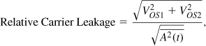
this phenomenon leads to two adverse effects. First, it distorts the signal constellation, raising the error vector magnitude at the TX output. For example, if Vout(t) represents a QPSK signal,
![]()
and is applied to an ideal direct-conversion receiver, then the baseband quadrature outputs suffer from dc offsets, i.e., horizontal and vertical shifts in the constellation (Fig. 4.92).
Figure 4.92 Effect of carrier feedthrough on received signal spectrum.
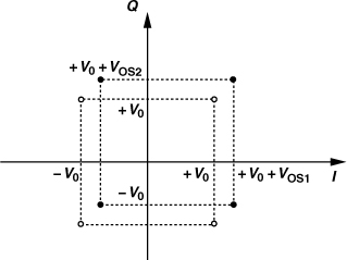
The second effect manifests itself if the output power of the transmitter must be varied across a wide range by varying the amplitude of the baseband signals. For example, as described in Chapter 3, CDMA mobiles must lower their transmitted power as they come closer to the base station so as to avoid the near-far effect. Figure 4.93(a) conceptually depicts the power control loop. The base station measures the power level received from the mobile and, accordingly, requests the mobile to adjust its transmitted power. With a short distance between the two, the mobile output power must be reduced to very low values, yielding the spectrum shown in Fig. 4.93(b) in the presence of carrier leakage. In this case, the carrier power dominates, making it difficult to measure the actual signal power. This issue arises if the mobile output power is adjusted by varying the baseband swings but not if the PA itself is adjusted.
Figure 4.93 (a) Power control feedback loop in CDMA, (b) effect of carrier leakage.
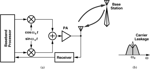
In order to reduce the carrier leakage, Eq. (4.140) suggests that the baseband signal swing, A(t), must be chosen sufficiently large. However, as A(t) increases, the input port of the upconversion mixers becomes more nonlinear. A compromise is therefore necessary. In stringent applications, the offsets must be trimmed to minimize the carrier leakage. As illustrated in Fig. 4.94, two DACs are tied to the baseband ports of the TX27 and a power detector (e.g., a rectifier or an envelope detector) monitors the output level, and its output is digitized. During carrier leakage cancellation, the baseband processor produces a zero output so that the detector measures only the leakage. Thus, the loop consisting of the TX, the detector, and the DACs drives the leakage toward zero, with the final settings of the DACs stored in the register.
Figure 4.94 Reduction of carrier leakage by baseband offset control.

How should the two DACs be adjusted so that the loop in Fig. 4.94 converges? An adaptive loop such as the least mean square (LMS) algorithm can perform this task. Alternatively, an “exhaustive” search can arrive at the optimum settings; e.g., for 8-bit DACs, only 256 × 256 possible combinations exist, and the system can try all to determine which combination yields the lowest leakage at the output. In this procedure, the system begins with, say, zero settings for both DACs, measures the carrier leakage, memorizes this value, increments one DAC by 1 LSB, measures the leakage again, and compares the result with the previous value. The new settings replace the previous ones if the new leakage is lower.
Mixer Linearity
Unlike downconversion mixers in a receiver, upconversion mixers in a transmitter sense no interferers. However, excessive nonlinearity in the baseband port of upconversion mixers can corrupt the signal or raise the adjacent channel power (Chapter 3). As an example, consider the GMSK signal expressed by Eq. (4.112) and suppose the baseband I/Q inputs experience a nonlinearity given by α1x + α3x3. The upconverted signal assumes the form [15]
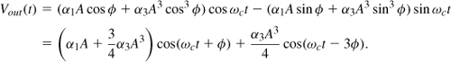
The second term also represents a GMSK signal but with a threefold modulation index, thereby occupying a larger bandwidth. Simulations indicate that this effect becomes negligible if the baseband port of the mixers experiences a nonlinearity less than 1% for the specified baseband swings [15].
For variable-envelope signals, A3(t) appears in both terms of Eq. (4.143), exacerbating the effect. The required mixer linearity is typically determined by simulations. However, in most cases (i.e., in a good design), as the baseband signal swings increase, the PA output begins to compress before the mixer nonlinearity manifests itself. This is explained below.
TX Linearity
The linearity of transmitters must be chosen according to the spectral regrowth (adjacent channel power) requirements and/or the tolerable distortion of the signal to be transmitted. As mentioned in Chapter 3, both of these effects become critical for variable-envelope modulation schemes. We defer the former to Chapter 12 and deal with the latter here.
The distortion of a variable-envelope signal is typically characterized by the compression that it experiences. As shown in Fig. 4.95, the signal is subjected to a nonlinear characteristic in simulations and it is determined how close its level can come to the 1-dB compression point while the degradation in the constellation or the bit error rate is negligible. For example, the average power of the 64-QAM OFDM signal in 802.11a must remain about 8 dB below P1dB of a given circuit. We say the circuit must operate at “8-dB back-off.” In other words, if a peak swing of V0 places the circuit at the 1-dB compression point, then the average signal swing must not exceed V0/2.51.
Figure 4.95 Variable-envelope signal applied to a compressive system.

In a TX chain, the signal may experience compression in any of the stages. Consider the example depicted in Fig. 4.96, where the signal levels (in dB) along the chain are also shown. Since the largest voltage swing occurs at the output of the PA, this stage dominates the compression of the TX; i.e., in a good design, the preceding stages must remain well below compression as the PA output approaches P1dB. To so ensure, we must maximize the gain of the PA and minimize the output swing of the predriver and the stages preceding it. This requirement places additional burden on the PA design (Chapters 12 and 13).
Figure 4.96 Level chart for the signals along a TX chain.
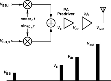
Solution:
![]()
The reader is encouraged to consider the special cases β3 = 0 or α3 = 0 and justify the results intuitively. It is interesting to note that if ![]() , the coefficient of x3 falls to zero and A1dB,in → ∞. This is because the compression in one stage is cancelled by the expansion in the other.
, the coefficient of x3 falls to zero and A1dB,in → ∞. This is because the compression in one stage is cancelled by the expansion in the other.
![]()
Oscillator Pulling
While the issues described above apply to most transmitter architectures, another one becomes particularly critical in direct-conversion topologies. As illustrated in Fig. 4.97(a), the PA output exhibits very large swings (20 Vpp for 1 W delivered to a 50-Ω load), which couple to various parts of the system through the silicon substrate, package parasitics, and traces on the printed-circuit board. Thus, it is likely that an appreciable fraction of the PA output couples to the local oscillator. Even if the PA is off-chip, the PA driver may still pull the LO. Note that the center frequency of the PA output spectrum is equal to ωLO in direct-conversion transmitters.
Figure 4.97 (a) Injection pulling of LO by PA in a direct-conversion TX, (b) conceptual illustration of injection into an oscillator.

Let us consider a “sliver” of the output spectrum centered at ωLO + Δω and model it by an impulse of equal energy [Fig. 4.97(b)]. We therefore inquire what happens if a sinusoid at a frequency of ω1 = ωLO + Δω is “injected” into an oscillator operating at a frequency of ωLO, where Δω ![]() ωLO. Called “injection pulling,” this phenomenon has been studied extensively [16, 17] and is analyzed in Chapter 8. In such a condition, the output phase of the oscillator, ϕout, is modulated periodically. In fact, as depicted in Fig. 4.98(a), ϕout remains around 90° (with respect to the input phase) for part of the period, subsequently experiencing a rapid 360° rotation. The input and output waveforms therefore appear as in Fig. 4.98(b). It can be proved that the output spectrum is heavily asymmetric [Fig. 4.98(c)], with most of the impulses located away from the input frequency, ωinj (=ωLO + Δω). Note that the spacing between the impulses is equal to the frequency of the phase variation in Fig. 4.98(a) and not equal to Δω.28
ωLO. Called “injection pulling,” this phenomenon has been studied extensively [16, 17] and is analyzed in Chapter 8. In such a condition, the output phase of the oscillator, ϕout, is modulated periodically. In fact, as depicted in Fig. 4.98(a), ϕout remains around 90° (with respect to the input phase) for part of the period, subsequently experiencing a rapid 360° rotation. The input and output waveforms therefore appear as in Fig. 4.98(b). It can be proved that the output spectrum is heavily asymmetric [Fig. 4.98(c)], with most of the impulses located away from the input frequency, ωinj (=ωLO + Δω). Note that the spacing between the impulses is equal to the frequency of the phase variation in Fig. 4.98(a) and not equal to Δω.28
Figure 4.98 (a) Behavior of LO output phase in the presence of injection pulling, (b) cycle slips in time domain, (c) resulting spectrum.

At what output power level does injection pulling become significant? The answer depends on several factors: (1) the internal voltage and current swings of the LO (the larger they are, the less is the effect of pulling); (2) the Q of the tank used in the oscillator; (3) whether the PA output is differential, in which case its coupling to the LO is 30–40 dB lower than if it is single-ended;29 (4) how much the feedback loop controlling the LO (the synthesizer) counteracts the pulling [17]; (5) the symmetry of the layout and the type of packaging. Nonetheless, for typical designs, as the PA output exceeds 0 dBm, injection pulling may prove serious.
In order to avoid injection pulling, the PA output frequency and the oscillator frequency must be made sufficiently different (e.g., by more than 20%), an impossible task in the architecture of Fig. 4.97. This principle has led to a number of transmitter architectures and frequency plans that are described below.
Noise in RX Band
As explained in Chapter 3, some standards (e.g., GSM) specify the maximum noise that a TX can transmit in the RX band. In a direct-conversion transmitter, the baseband circuits, the upconverter, and the PA may create significant noise in the RX band. To resolve this issue, “offset-PLL” transmitters can be used (Chapter 9).
4.3.3 Modern Direct-Conversion Transmitters
Most of today’s direct-conversion transmitters avoid an oscillator frequency equal to the PA output frequency. To avoid confusion, we call the former the LO frequency, ωLO, and the latter, the carrier frequency, ωc. The task is accomplished by choosing ωLO sufficiently far from ωc and deriving ωc from ωLO by operations such as frequency division and mixing.
Figure 4.99 depicts a common example where ωLO = 2ωc. A divide-by-2 circuit follows the LO, thereby generating ωLO/2 with quadrature phases. This architecture is popular for two reasons: (1) injection pulling is greatly reduced, and (2) the divider readily provides quadrature phases of the carrier, an otherwise difficult task (Chapter 8).
Figure 4.99 Use of an LO running at twice the carrier frequency to minimize LO pulling.

The architecture of Fig. 4.99 does not entirely eliminate injection pulling. Since the PA nonlinearity produces a finite amount of power at the second harmonic of the carrier, the LO may still be pulled. Nonetheless, proper layout and isolation techniques can suppress this effect.
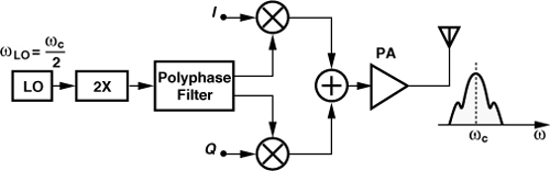
The principal drawback of the architecture of Fig. 4.99 stems from the speed required of the divider. Operating at twice the carrier frequency, the divider may become the speed bottleneck of the entire transceiver. (We deal with divider design in Chapter 10.) Nevertheless, as seen in the following discussion, other transmitter architectures suffer from more serious drawbacks. Thus, even a substantial effort on divider design to enable this architecture is well justified.
Another approach to deriving frequencies is through the use of mixing. For example, mixing the outputs of two oscillators operating at ω1 and ω2 can yield ω1 + ω2 or ω1 − ω2. Nonetheless, as with the receivers studied in Section 4.2, it is desirable to employ a single oscillator and utilize division to obtain subharmonics. To this end, let us consider the arrangement shown in Fig. 4.101(a), where the oscillator frequency is divided by 2 and the two outputs are mixed. The result contains components at ω1±ω1/2 with equal magnitudes. We may call one the “image” of the other with respect to ω1.
Figure 4.101 (a) Mixing of an LO output with half of its frequency, (b) effect of two sidebands on transmitter output.
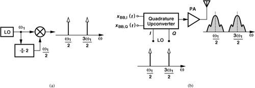
Can both components be retained? In a transmitter using such an LO waveform, the upconverter output would contain, with equal power, the signal spectrum at both carrier frequencies [Fig. 4.101(b)]. Thus, half of the power delivered to the antenna is wasted. Furthermore, the power transmitted at the unwanted carrier frequency corrupts communication in other channels or bands. One component (e.g., that at ω1/2) must therefore be suppressed.
It is difficult to remove the unwanted carrier by means of filtering because the two frequencies differ by only a factor of 3. For example, in Problem 4.24 we show that a second-order LC filter resonating at 3ω1/2 attenuates the component at ω1/2 by a factor of 8Q/3. For a Q in the range of 5 to 10, this attenuation amounts to 25 to 30 dB, sufficient for minimizing the waste of power in the unwanted sideband but inadequate for avoiding corruption of other channels. The other issue is that the output in Fig. 4.101(a) is not available in quadrature form.
An alternative method of suppressing the unwanted sideband incorporates “single-sideband” (SSB) mixing. Based on the trigonometric identity cos ω1t cos ω2t − sin ω1t sin ω2t = cos(ω1 + ω2)t and illustrated in Fig. 4.102(a), SSB mixing involves multiplying the quadrature phases of ω1 and ω2 and subtracting the results—just as realized by the quadrature upconverter of Fig. 4.88. We denote an SSB mixer by the abbreviated symbol shown in Fig. 4.102(b). Of course, gain and phase mismatches lead to an unwanted sideband, as expressed by Eq. (4.127). With typical mismatches, P−/P+ falls in the vicinity of 30 to 40 dB, and filtering by a second-order LC stage attenuates the sideband by another 25 to 30 dB.
Figure 4.102 Single-sideband mixer (a) implementation, (b) simplified symbol.
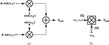
In addition to the image sideband, the harmonics of the input frequencies also corrupt the output of an SSB mixer. For example, suppose each mixer in Fig. 4.102(a) exhibits third-order nonlinearity in the port sensing A sin ω1t or A cos ω1t. If the nonlinearity is of the form α1x + α3x3, the output can be expressed as

The output spectrum contains a spur at 3ω1 − ω2. Similarly, with third-order nonlinearity in the mixer ports sensing sin ω2t and cos ω2t, a component at 3ω2 − ω1 arises at the output. The overall output spectrum (in the presence of mismatches) is depicted in Fig. 4.103.
Figure 4.103 Output spectrum of SSB mixer in the presence of nonlinearity and mismatches.
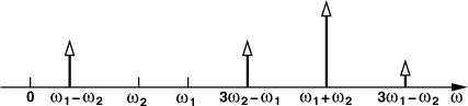
Figure 4.104 shows a mixer example where the port sensing Vin1 is linear while that driven by Vin2 is nonlinear. As explained in Chapter 2, the circuit multiplies Vin1 by a square wave toggling between 0 and 1. That is, the third harmonic of Vin2 is only one-third of its fundamental, thus producing the strong spurs in Fig. 4.103.
How serious are the above spurs? In a typical mixer design (Chapter 6), it is possible to linearize only one port, thus maintaining a small third harmonic in that port. The other is highly nonlinear so as to retain a reasonable gain (or loss). We therefore conclude that, between the two spurs at 3ω1 − ω2 and 3ω2 − ω1, only one can be reduced to acceptably low levels while the other remains only 10 dB (a factor of one-third) below the desired component. As an example, if ω2 = ω1/2, then 3ω1 − ω2 = 5ω1/2 and 3ω2 − ω1 = ω1/2; we can linearize the port sensing ω2 to suppress the latter, but the former still requires substantial filtering.
For use in a direct-conversion TX, the SSB mixer must provide the quadrature phases of the carrier. This is accomplished by noting that sin ω1t cos ω2t+cos ω1t sin ω2t = sin(ω1 + ω2)t and duplicating the SSB mixer as shown in Fig. 4.105.
Figure 4.105 SSB mixer providing quadrature outputs.
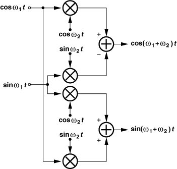
Figure 4.106 shows a direct-conversion TX with SSB mixing for carrier generation. Since the carrier and LO frequencies are sufficiently different, this architecture remains free from injection pulling.30 While suppressing the carrier sideband at ω1/2, this architecture presents two drawbacks: (1) the spurs at 5ω1/2 and other harmonic-related frequencies prove troublesome, and (2) the LO must provide quadrature phases, a difficult issue (Chapter 8).
Figure 4.106 Direct-conversion TX using SSB mixing in LO path.
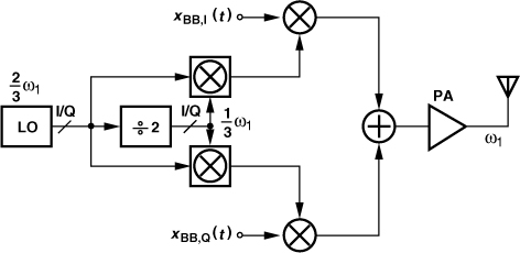
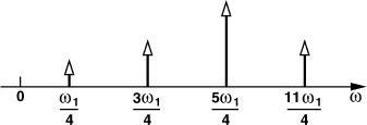
4.3.4 Heterodyne Transmitters
Another approach to avoiding injection pulling involves performing the signal upconversion in two steps so that the LO frequency remains far from the PA output spectrum. Shown in Fig. 4.108, such a TX topology is the “dual” of the heterodyne receiver studied in Section 4.2.1. Here, the baseband I and Q signals are upconverted to an IF of ω1, and the result is mixed with ω2 and hence translated to a carrier frequency of ω1 + ω2. Since the second mixer also produces an output at ω1 − ω2, a band-pass filter follows this stage. As with the receiver counterpart, one advantage of this architecture is that the I/Q upconversion occurs at a significantly lower frequency than the carrier, exhibiting smaller gain and phase mismatches. The equations quantifying the effect of mismatches are the same as those derived in Section 4.3.2 for the direct-conversion TX.
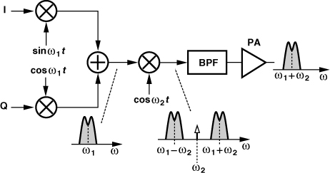
In analogy with the sliding-IF receiver architecture of Fig. 4.26(a), we eliminate the first oscillator in the above TX and derive the required phases from the second oscillator (Fig. 4.109). The carrier frequency is thus equal to 3ω1/2. Let us study the effect of nonidealities in this architecture. We call the LO waveforms at ω1/2 and ω1 the first and second LOs, respectively.
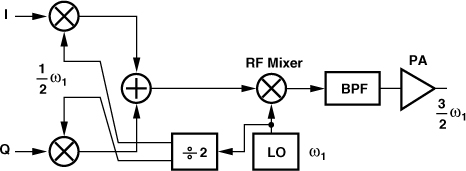
Carrier Leakage
The dc offsets in the baseband yield a component at ω1/2 at the output of the quadrature upconverter, and the dc offset at the input of the RF mixer produces another component at ω1 (Fig. 4.110). The former can be minimized as described in Section 4.3.2. The latter, and the lower sideband at ω1/2, must be removed by filtering. The leakage at ω1 is closer to the upper sideband than the lower sideband is, but it is also much smaller than the lower sideband. Thus, the filter following the RF mixer must be designed to attenuate both to acceptably low levels.
Figure 4.110 Carrier leakage in heterodyne TX.
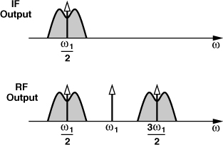
Mixing Spurs
The heterodyne TX of Fig. 4.109 displays various mixing spurs that must be managed properly. The spurs arise from two mechanisms: the harmonics of the first LO and the harmonics of the second LO.
The quadrature upconverter mixes the baseband signals with the third and fifth harmonics of the first LO,31 thus creating replicas of the signal spectrum at ω1/2, 3ω1/2, and 5ω1/2. The result is shown in Fig. 4.111(a) for an asymmetrically-modulated signal. Note that the harmonic magnitudes follow a sinc envelope if the mixers operate as the switching network depicted in Fig. 4.104. In other words, the magnitudes of the replicas at 3ω1/2 and 5ω1/2 are one-third and one-fifth of the desired signal magnitude, respectively. Upon mixing with the second LO (ω1), the components in Fig. 4.111(a) are translated up and down by an amount equal to ω1, yielding the spectrum illustrated in Fig. 4.111(b). Interestingly, the desired sideband at +3ω1/2 is enhanced by a smaller replica that results from the mixing of 5ω1/2 and ω1. The unwanted sidebands at ω1/2, 5ω1/2, and 7ω1/2 must be suppressed by an RF band-pass filter.
Figure 4.111 Spurs at (a) IF and (b) RF outputs of a heterodyne TX.
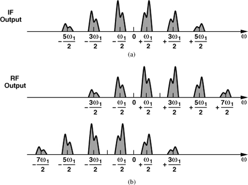
The second mechanism relates to the harmonics of the second LO. That is, the spectrum shown in Fig. 4.111(a) is mixed with not only ω1 but 3ω1, 5ω1, etc. Illustrated in Fig. 4.112 is the resulting output, revealing that, upon mixing with +3ω1, the IF sideband at −3ω1/2 is translated to +3ω1/2, thereby corrupting the wanted sideband (if the modulation is asymmetric). Similarly, the IF sideband at −5ω1/2 is mixed with +5ω1 and falls atop the desired signal.
Figure 4.112 Effect of harmonics of second LO on TX output.

How serious is this corruption? Since the IF sideband at −3ω1/2 is 10 dB below the desired signal, and since mixing with 3ω1 entails another 10 dB attenuation (why?), the level of corruption is at −20 dB. This value is acceptable only for modulation schemes that require a moderate SNR (10–12 dB) (e.g., QPSK) or systems with a moderate bit error rate (e.g., 10−2). Even in these cases, some IF filtering is necessary to suppress the unwanted sidebands before they are upconverted to RF and fall into other users’ channels.
The unwanted sideband at ω1 − ω1/2 produced by the RF mixer in Fig. 4.109 can be greatly suppressed through the use of SSB mixing. To this end, the IF signal must be generated in quadrature form. Figure 4.113 shows such a topology [15, 18], where two quadrature upconverters provide the quadrature components of the IF signal:
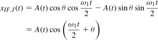

Figure 4.113 Use of baseband quadrature SSB mixing and IF SSB mixing to reduce the unwanted component.

The RF SSB mixer then translates the result to ω1 + ω1/2. The reader is encouraged to study the mixing spurs in this architecture.
While attenuating the sideband at ω1 −ω1/2, the architecture of Fig. 4.113 suffers from three drawbacks: (1) the oscillator must provide quadrature outputs, a difficult issue (Chapter 8), (2) the circuit employs twice as many mixers as those in the original architecture (Fig. 4.109), and (3) the loading seen by the ÷2 circuit is doubled. The first issue can be alleviated by operating the oscillator at 2ω1 and following it with a ÷2 stage, but such a design is only slightly simpler than the direct-conversion architecture of Fig. 4.106.
Our study of the heterodyne sliding-IF TX has thus far assumed that the first LO frequency is half of the second LO frequency. It is possible to replace the ÷2 circuit with a ÷4 stage so as to produce the IF signal at ω1/4 and the RF output at ω1 + ω1/4 = 5ω1/4 [19]. We study the spurious effects in such an architecture in Problem 4.25.
4.3.5 Other TX Architectures
In addition to the TX architectures described above, several others find usage in some applications. These include “offset PLL” topologies, “in-loop modulation” systems, and “polar modulation” transmitters. We study the first two in Chapter 10 and the last in Chapter 12.
4.4 OOK Transceivers
“On-off keying” (OOK) modulation is a special case of ASK where the carrier amplitude is switched between zero and maximum. Transceivers employing OOK lend themselves to a compact, low-power implementation and merit some study here. Figure 4.114 illustrates two TX topologies. In Fig. 4.114(a), the LO is directly turned on and off by the binary baseband data. If the LO swings are large enough, the PA also experiences relatively complete switching and delivers an OOK waveform to the antenna. In contrast to the transmitter architectures studied in the previous sections, OOK does not require quadrature baseband or LO waveforms or a quadrature upconverter. Of course, it is also less bandwidth-efficient as unshaped binary pulses modulated on one phase of the carrier occupy a wide spectrum. Nonetheless, the simplicity of the architecture makes it attractive for low-cost, low-power applications.
Figure 4.114 OOK TX with (a) direct LO switching (b) PA switching.
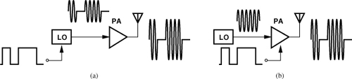
The principal issue in the TX of Fig. 4.114(a) is that the LO cannot be easily controlled by a phase-locked loop (Chapter 9). The TX of Fig. 4.114(b), on the other hand, keeps the LO on and directly switches the PA. We study the injection-pulling properties of the two architectures in Problem 4.29.
OOK receivers are also simple and compact. As shown in Fig. 4.115, an LNA followed by an envelope detector can recover the binary data, with no need for an LO. Of course, such a receiver has little tolerance of interferers.

References
[1] B. Razavi et al., “Multiband UWB Transceivers,” Proc. CICC, pp. 141–148, Sept 2005.
[2] B. Razavi, “Design Considerations for Direct-Conversion Receivers,” IEEE Trans. Circuits and Systems, vol. 44, pp. 428–435, June 1997.
[3] A. A. Abidi, “Direct-conversion Radio Transceivers for Digital Communications,” IEEE Journal of Solid-State Circuits, vol. 30, pp. 1399–1410, Dec. 1995.
[4] R. Hartley, “Modulation System,” US Patent 1,666,206, April 1928.
[5] D. K. Weaver, “A Third Method of Generation and Detection of Single-Sideband Signals,” Proc. IRE, vol. 44, pp. 1703–1705, Dec. 1956.
[6] J. Rudell et al., “A 1.9-GHz Wideband IF Double Conversion CMOS Receiver for Cordless Telephone Applications,” IEEE Journal of Solid-State Circuits, vol. 32, pp. 2071–2088, Dec. 1997.
[7] L. Der and B. Razavi, “A 2-GHz CMOS Image-Reject Receiver with LMS Calibration,” IEEE Journal of Solid-State Circuits, vol. 38, pp. 167–175, Feb. 2003.
[8] M. Gingell, “Single-Sideband Modulation Using Sequence Asymmetric Polyphase Networks,” Elec. Comm., vol. 48, pp. 21–25, 1973.
[9] S. Lerstaveesin and B. S. Song, “A Complex Image Rejection Circuit with Sign Detection Only,” IEEE J. Solid-State Circuits, vol. 41, pp. 2693–2702, Dec. 2006.
[10] J. Crols and M. S. J. Steyaert, “A Single-Chip 900-MHz CMOS Receiver Front End with a High-Perfromance Low-IF Topology,” IEEE J. Solid-State Circuits, vol. 30, pp. 1483–1492, Dec. 1995.
[11] F. Behbahani et al., “CMOS Mixers and Polyphase Filters for Large Image Rejection,” IEEE J. Solid-State Circuits, vol. 36, pp. 873–887, June 2001.
[12] J. Crols and M. S. J. Steyaert, “Low-IF Topologies for High-Performance Analog Front Ends of Fully Integrated Receivers,” IEEE Tran. Circuits and Sys., II, vol. 45, pp. 269–282, March 1998.
[13] K. Feher, Wireless Digital Communications, New Jersey: Prentice-Hall, 1995.
[14] R. Steele, Ed., Mobile Radio Communications, New Jersey: IEEE Press, 1992.
[15] B. Razavi, “A 900-MHz/1.8-GHz CMOS Transmitter for Dual-Band Applications,” IEEE Journal of Solid-State Circuits, vol. 34, pp. 573–579, May 1999.
[16] R. Adler, “A Study of Locking Phenomena in Oscillators,” Proc. of the IEEE, vol. 61, No. 10, pp. 1380–1385, Oct. 1973.
[17] B. Razavi, “A Study of Injection Locking and Pulling in Oscillators,” IEEE J. of Solid-State Circuits, vol. 39, pp. 1415–1424, Sep. 2004.
[18] M. Zargari et al., “A 5-GHz CMOS Transceiver for IEEE 802.11a Wireless LAN Systems,” IEEE J. of Solid-State Circuits, vol. 37, pp. 1688–1694, Dec. 2002.
[19] S. A. Sanielevici et al., “A 900-MHz Transceiver Chipset for Two-Way Paging Applications,” IEEE J. of Solid-State Circuits, vol. 33, pp. 2160–2168, Dec. 1998.
[20] M. Conta, private communication, Feb. 2011.
[21] B. Razavi, “A 5.2-GHz CMOS Receiver with 62-dB Image Rejection,” IEEE Journal of Solid-State Circuits, vol. 36, pp. 810–815, May 2001.
[22] A. Parsa and B. Razavi, “A New Transceiver Architecture for the 60-GHz Band,” IEEE Journal of Solid-State Circuits, vol. 44, pp. 751–762, Mar. 2009.
Problems
4.1. For the sliding-IF architecture of Fig. 4.26(a), assume the ÷2 circuit is replaced with a ÷4 circuit.
(a) Determine the required LO frequency range and steps.
(b) Determine the image frequency range.
4.2. Since the image band of the sliding-IF receiver of Fig. 4.26(a) is narrower than the signal band, is it possible to design an 11g receiver whose image is confined to the GPS band? Explain your reasoning.
4.3. A sliding-IF receiver with fLO = (2/3)fin is designed for the 11g band. Determine some of the mixing spurs that result from the harmonics of the first LO and the second LO. Assume the second IF is zero.
4.4. Consider the 11g sliding-IF receiver shown in Fig. 4.116.
(a) Determine the required LO frequency range.
(b) Determine the image frequency range.
(c) Is this architecture preferable to that in Fig. 4.26(a)? Why?
Figure 4.116 Sliding-IF RX for 11g.
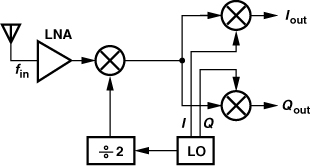
4.5. Determine some of the mixing spurs in the architecture of Fig. 4.116.
4.6. The sliding-IF architecture shown in Fig. 4.117 is designed for the 11a band.
(a) Determine the image band.
(b) Determine the interferer frequencies that can appear in the output baseband as a result of mixing with the third harmonic of the first LO or the third harmonic of the second LO.
Figure 4.117 Sliding-IF RX for 11a.
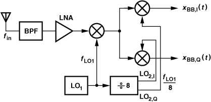
4.7. Figure 4.118 shows a “half-RF” architecture, where fLO = f − in/2 [21, 22].
(a) Assume the RF input is an asymmetrically-modulated signal. Sketch the spectra at the first and second IFs if the mixers are ideal multipliers.
(b) Repeat part (a) but assuming that the RF mixer also multiplies the RF signal by the third harmonic of the LO.
(c) The flicker noise of the LNA may be critical here. Explain why.
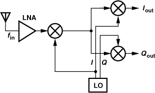
4.8. Suppose an AM signal, A(t) cos ωct, is applied to a single mixer driven by an LO.
(a) If the LO waveform is given by cos ωct, determine the baseband signal.
(b) If the LO waveform is given by sin ωct, what happens? Why does this indicate the need for quadrature downconversion?
4.9. In this problem we wish to study an interesting effect that arises from LO leakage in direct-conversion receivers [20]. Consider the LO leakage in a direct-conversion receiver, V0 cos ωLOt. Suppose this leakage is added to an amplitude-modulated interferer, Vint(t) cos ωintt, and the result experiences third-order nonlinearity in the LNA (or downconversion mixer).
(a) Determine the components near the carrier at the LNA output.
(b) Determine the resulting baseband components and whether they corrupt the desired signal.
4.10. In Example 4.24, how much gain must precede the given noise spectrum so that the penalty remains below 1 dB?
4.11. In Example 4.24, what flicker noise corner frequency is necessary if the penalty must remain below 1 dB?
4.12. An ASK waveform is applied to a direct-conversion receiver. Plot the baseband I and Q waveforms.
4.13. Does the quadrature mixing of Fig. 4.59(a) perform a Hilbert transform if the upconverted outputs at ωc + ωLO are considered?
4.14. Repeat the analysis in Fig. 4.59 if ωIF > ωc.
4.15. Does the Hartley architecture cancel the image if the IF low-pass filters are replaced with high-pass filters and the upconverted components are considered?
4.16. In the architecture of Fig. 4.64, assume the two resistors have a mismatch of ΔR. Compute the IRR.
4.17. Prove that the IRR of the Hartley architecture is given by (ωIF/Δω)2 at an intermediate frequency of ωIF + ω if ωIF = (R1C1)−1.
4.18. Considering only the thermal noise of the resistors in Fig. 4.64 and assuming a voltage gain of A1 for each mixer, determine the noise figure of the receiver with respect to a source impedance of RD.
4.19. In the Weaver architecture of Fig. 4.67, both quadrature downconversions were performed with low-side injection. Study the other three combinations of high-side and low-side injection with the aid of signal spectra at nodes A-F.
4.20. Figure 4.119 shows three variants of the Hartley architecture. Explain which one(s) can reject the image.
Figure 4.119 Possible variants of Hartley RX.
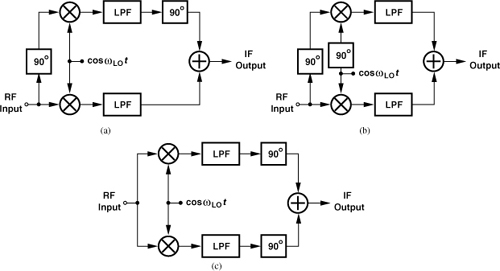
4.21. If sin ωLOt and cos ωLOt in the Hartley architecture are swapped, does the RX still reject the image?
4.22. Repeat the above problem for the first or second LO in a Weaver architecture.
4.23. Using Eq. (4.96), compute the IRR of the receiver shown in Fig. 4.77(b) at an IF of ω + Δω.
4.24. Assume a second-order parallel RLC tank is excited by a current source containing a component at ω0 and another at 3ω0. Prove that, if the tank resonates at 3ω0, then the first harmonic is attenuated by approximately a factor of 8Q/3 with respect to the third harmonic.
4.25. If the ÷2 circuit in Fig. 4.109 is replaced with a ÷4 circuit, study the spurious components arising from the third and fifth harmonics of the first and second LO frequencies.
4.26. The simplified Hartley architecture shown in Fig. 4.120 incorporates mixers having a voltage conversion gain of Amix and an infinite input impedance. Taking into account only the noise of the two resistors, compute the noise figure of the receiver with respect to a source resistance of RS at an IF of 1/(R1C1).
Figure 4.120 Simplified Hartley RX.
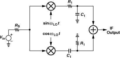
4.27. A dual-band receiver employing a Weaver architecture is shown in Fig. 4.121. The first LO frequency is chosen so as to create high-side injection for the 2.4-GHz band and low-side injection for the 5.2-GHz band. (The receiver operates only in one band at a given time.) Neglect the noise and nonlinearity of the receiver itself and assume an SNR of 20 dB is required for the signal to be detected properly. The Weaver architecture provides an image rejection ratio of 45 dB.
(a) Suppose the receiver must detect a −85-dBm signal in the 2.4-GHz mode while receiving at the same antenna a −10-dBm 5.2-GHz component as well. Determine the amount of rejection required of BPF1 at 5.2 GHz.
(b) Suppose the receiver operates in the 5.2-GHz band but it also picks up a strong component at 7.2 GHz. It is possible for this component to be mixed with the third harmonics of LO1 and LO2 and appear in the baseband. Does the Weaver architecture prohibit this phenomenon? Explain in detail.
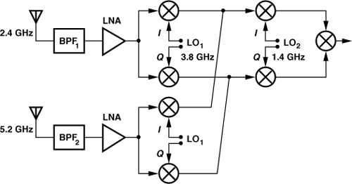
4.28. Consider the single-sideband mixer shown in Fig. 4.122. In the ideal case, the output has only one component at ω1 + ω2. Now suppose the ports sensing ω2 suffer from third- and fifth-order nonlinearity. Plot the output spectrum if (a) ω1 > 3ω2 or (b) ω1 < 3ω2. Identify the frequency of each component.
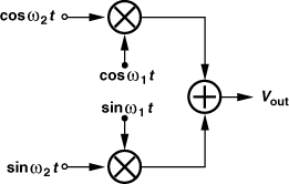
4.29. Explain why injection pulling is more serious in Fig. 4.114(b) than in Fig. 4.114(a).