Chapter 2
ESD Architecture and Floorplanning
One of the most fundamental issues and challenges in the ESD design discipline is ESD architecture and floorplanning. The integration of the devices, circuits, sub-functions, and cores is critical to the success of EOS and ESD robust designs. In each application space, the floorplan and layout of a semiconductor chip may be different, leading to unique challenges for ESD protection design [1–6]. Whether it is DRAM [10–12], SRAM [1–3, 6], NVRAM, microprocessor [1–4, 12–20], CPU, ASICs [1–6], or semiconductor foundry, each has unique challenges for ESD design. Whether it is single voltage, mixed voltage or mixed signal, the ESD design strategy and architecture has to be modified. Additionally, CMOS, BiCMOS, and BCD technology produce digital [1–20], analog [21–24], power [25–29], and RF [30–32] applications with integration, layout, and design.
In this text, one of the goals is to teach how to construct a semiconductor chip to achieve an ESD robust implementation. Significant focus in publications address semiconductor device physics and ESD circuits, but the subject of how to integrate all the elements into a given product has limited exposure.
The ordering of materials in this text is constructed in the fashion that a semiconductor chip is assembled. In this chapter, we will begin by discussing the architecture and layout floorplanning for different chip architectures. The discussion will address both peripheral and “array” I/O configurations. For peripheral I/O architectures, architectures with aligned I/O to staggered I/O will be shown. For array I/O configurations, implementations of off-chip driver “banks,” nibble architectures, to single I/O circuits in the chip will be discussed. In the chapter, issues of power bus architectures will also be shown. Mixed-voltage implementations, to mixed-signal architectures, and global floorplanning will be discussed [2–4]. In future chapters, each chapter will go into greater depth for the ESD circuits, the power bus, the guard rings, and chip integration.
In semiconductor chip design, the circuit design team follows an application performance and specification objectives. The ESD specifications and objectives are part of the original design definition for the product. The core functions are defined, and the interface circuitry between the semiconductor chip and outside is also addressed. Once these objectives are established, the placement of the cores and the interface circuitry are defined. As part of the floorplanning process, the I/O interface circuitry placement and power bus are decided. At this time, the chapter will deviate to discuss the options for I/O placement, and how the ESD elements and power are integrated into the I/O floorplan.
In semiconductor chip design, there are two fundamental classes of I/O configurations. These two different architectures have a significant effect on the ESD design architectures. We will refer to them as “peripheral I/O” and “array I/O” architectures [2, 3].
In the “peripheral I/O” architecture, the signal and power bond pads are placed on the edge of the semiconductor chip. The primary reason is that, in the majority of cases, the I/O circuitry must interface with other chips, a system, or the outside environment. The packages use wire bonds between the silicon chip and the package. This decision is dependent on the cost, the package size, and the pin count of the semiconductor chip.
Figure 2.1 shows an example of the layout and floorplan for a peripheral I/O architecture. The width of the I/O design and spacing between the I/O cells is limited by the bond pad size, the bond pad design rules, and wire bond rules. In a “peripheral I/O limited design,” the maximum number of I/O standard cells and power cells are defined according to the allowed rules of the technology and package, and technology definition rules.
Figure 2.1 Peripheral I/O design
In the peripheral I/O architecture, ESD elements are placed with the circuit in the custom or standard I/O cell. The peripheral I/O architecture must contain the input, output, and bi-directional circuitry, as well as service functions, and power pads. The ESD networks are inherently integrated with the I/O cells, and the power pads.
2.2.1 Pad-Limited Peripheral I/O Design Architecture
In semiconductor chips, the majority of products and applications encountered are designs with peripheral I/O circuitry. Product application types that are typically peripheral I/O can vary from memory, logic, digital, analog, mixed signal, mixed voltage, and power applications [1–30]. Some applications can not have bond pads, wiring, and other circuits in the center of the chip, such as CMOS imaging applications. In other applications, there is a limit on how far one can wire bond into a semiconductor chip. There are different cases of peripheral I/O chips of interest – one is the pad-limited peripheral I/O architecture.
In peripheral I/O design, the wire bonds and packaging requirements limit the number of I/O placed on the periphery of the semiconductor chip. Limitations to the number of I/O on the periphery of a chip are as follows:
- Bond pad dimensions (width and length).
- Bond pad to bond pad spacing.
- Bond pad to active circuitry requirements.
Figure 2.2 shows an example of a pad-limited peripheral I/O design architecture. From an ESD design synthesis perspective, the bond pad dimensions influence the following:
- Placement of the ESD network.
- Form factor of the ESD network.
- Electrical connections between the bond pad and the ESD network.
- Electrical connections between the ESD network and the power rails.
- Guard ring placement.
- ESD network interaction with I/O circuitry.
- Latchup considerations for the ESD network and adjacent elements.
In peripheral pad I/O design, ESD elements can be placed adjacent to the bond pad, or under the bond pad.
Figure 2.2 Pad-limited peripheral I/O design

2.2.2 Pad-Limited Peripheral I/O Design Architecture – Staggered I/O
In peripheral I/O design, the wire bonds and packaging requirements limit the number of I/O placed on the periphery of the semiconductor chip. To increase the number of I/O cells, one solution is peripheral I/O staggering of the cells. Figure 2.3 shows an example of a peripheral I/O design architecture with staggered I/O. With the staggering of the I/O cells, the bond wire to bond wire spacing is increased, allowing an increase in the number of I/O cells. This allows for the reduction of the pad size, and the pitch of the I/O circuitry. The I/O circuit standard cell is compensated by changing its aspect ratio, and the placement of the power buses.
Figure 2.3 Peripheral I/O architecture with staggered I/O circuitry

In the staggered I/O configuration, ESD design synthesis and latchup considerations must address the following:
- Placement of the input location relative to the ESD element.
- Guard ring resistance between the power connection and the worst case resistance point of the guard ring.
- Standard cell to standard cell latchup (PFET of the first standard cell, and NFET of the second standard cell).
2.2.3 Core-Limited Peripheral I/O Design Architecture
In semiconductor chips, some products and applications encountered are core-limited designs with peripheral I/O circuitry. Product application types that are typically peripheral I/O with core-limited applications are low pin-count chips that require large arrays, or large devices. These can be CMOS image processing chips, memory, mixed signal, mixed voltage, and power applications. For example, in a CMOS image processing chip, it can not have bond pads, wiring, and other circuits in the center of the chip; it is also desirable to have the size of the array as large as possible. In power electronics, there are applications with only a few pins, but large devices. In these architectures, the area on the periphery is not constrained to bond pad dimensions, bond pad to bond pad spacing, and other technology limits. They provide significant area in the periphery for support networks, logic, de-coupling capacitors, and ESD networks. Figure 2.4 shows an example of a core-limited peripheral I/O design architecture. Core-limited peripheral I/O ESD design is significantly different from pad-limited peripheral I/O design due to many of the constraints not being present, providing design freedom in the architecture, floorplan, orientation, size, form factor, and footprint of the ESD networks.
Figure 2.4 Core-limited peripheral I/O design

2.3 Lumped ESD Power Clamp in Peripheral I/O Design Architecture
In ESD design synthesis of a peripheral I/O architecture, ESD power clamps are placed in the “pad ring” with the signal bond pads, power bond pads, and power bus. The whole-chip ESD performance is dependent on how the ESD power clamps are distributed along the power rail. ESD power clamps can be integrated into the individual signal pad “cell,” or more commonly placed as a “lumped” element in the semiconductor chip. In this section, the integration of lumped ESD power clamps is discussed.
2.3.1 Lumped ESD Power Clamp in Peripheral I/O Design Architecture in the Semiconductor Chip Corners
In ESD design synthesis, ESD power clamps are placed in the “pad ring” with the signal bond pads, power bond pads, and power buses. In many chip designs, the corners of the semiconductor chip are not utilized. The reasons for not using the corners are as follows:
- Restrictions on placing signal pins in the corner.
- Mechanical stress on the chip corners influencing the circuitry.
- Photolithography control on the chip corners.
- Placement of identification markings.
- Corners are “white space” regions existing in the semiconductor chips.
It is common practice in ESD design synthesis to utilize this corner area for placement of the ESD power clamps between the power and ground circuitry. Figure 2.5 shows an example of a semiconductor chip with placement of the ESD power clamps in the corners. This ESD design synthesis is very common in very small semiconductor chips, below 5 mm × 5 mm. Placement of the ESD elements in the corners of large microprocessors or ASIC implementations is more limited due to the series resistance of the power bus.
Figure 2.5 Floorplan with ESD power clamps in the semiconductor chip corners
2.3.2 Lumped ESD Power Clamp in Peripheral I/O Design Architecture – Power Pads
In peripheral I/O design, in very large semiconductor chips, or small semiconductor chips that require high ESD robustness, the ESD power clamps are placed at a higher spatial frequency. A natural placement of the ESD power clamps is in the peripheral “standard cell” regions where VDD or VSS power pins are required. In some ASICs, microprocessor or standard cell foundry methodologies, it is a requirement to place VDD and VSS power pins at a given frequency for a given number of I/O cells. For example, in some methodologies, it is a requirement to place a “power pin” adjacent to every fifth I/O standard cell. Placement of the ESD power clamps within the “power cell” or “power book” allows for the local placement of ESD networks within a given periodicity of every I/O signal pin. Additionally, the placement of the ESD power clamps can naturally be integrated into the design methodology as part of the power pin frequency requirements. In this system, the complete ESD power clamp network is contained throughout the periphery of the semiconductor chip design, in a given periodicity.
2.4 Lumped ESD Power Clamp in Peripheral I/O Design Architecture – Master/Slave ESD Power Clamp System
In the previous section, the complete ESD power clamp is placed in a given “power cell” or “power book” in a standard cell environment. In this methodology, it allows for the local placement of ESD networks within a given periodicity of every I/O signal pin. In this method, the initiation or “triggering” of each power clamp is independent of the ESD power clamp itself.
A different ESD methodology is to use a “master/slave” ESD design methodology. In a master/slave concept, a single ESD power clamp has the trigger or initiation circuit only in one ESD power clamp (e.g., the master ESD power clamp). Figure 2.6 shows a circuit schematic representation of the ESD master/slave implementation [24]. In the ESD network, a single trigger network is contained within the master ESD power clamp. The trigger network signal is sent to the slave ESD power clamp implementations.
Figure 2.6 Master/slave ESD power clamps

Figure 2.7 shows an example floorplan of the master/slave system with the ESD power clamps in the corner of the chip. In the master/slave ESD system, the interconnection between the master trigger and the slave networks is shown. An advantage of the master/slave system is that a single trigger initiates the entire system. A second advantage is that the slave clamps can be placed at a high spatial frequency along the periphery. A disadvantage of the master/slave system is that the additional bus is required to transfer the signal from the master ESD power clamp to the slave clamps.
Figure 2.7 Master/slave ESD power clamps design layout and floorplan

As the number of circuits increases on a semiconductor chip, the number of signal pins increases. For large semiconductor chips, floorplans are modified to “array I/O” where the inputs, outputs, and bi-directional circuitry is placed in the interior of a semiconductor chip. This architecture brings new challenges for ESD design synthesis.
In an array I/O semiconductor architecture, the package is designed in an array of solder balls equally spaced and arranged. For example, in a 1000-pin semiconductor chip, an array of 100 × 100 solder balls and bond pads is arranged on the top level. The metal layer below the bond pads is known as the “transfer wire” level, which is the method of connecting from the bond pads to the I/O circuitry in the semiconductor chip.
In this methodology, the bond pad is separated from the I/O circuitry and ESD network. In some cases, the bond pad is directly over the I/O cell; and in other cases, it is not. The I/O cell is placed in the “cores” surrounded by dense CMOS logic, and gate array circuitry (Figure 2.8). In this methodology, for impedance matching, the resistance in series must be matched for identical circuits. The design method addresses the matching by adjusting the series resistance using a resistor element, which compensates for the metal wire resistance. To have impedance matching of an off-chip driver (OCD), the impedance consists of the interconnect resistance, the corrective ballast resistance, and the OCD circuit impedance. The corrective ballast resistor would be adjusted to provide the matching. In most ESD architectures, the ESD ballast resistor is fixed; in this methodology, it is variable based on spatial placement of the I/O cell.
Figure 2.8 Array I/O architecture

The ESD floorplan and issues are as follows:
- Interconnects: Metal interconnect width and via number limitations due to transfer wire.
- Interconnects: Wire width limitation for performance in high-speed input receivers.
- Ballast Resistor: Automated ballast resistor variations.
- ESD Power Clamp: Placement of ESD power clamps.
- Latchup: Placement of I/O in dense logic.
- I/O Footprint: I/O cell aspect ratio may differ from the peripheral I/O standard cell.
2.5.1 Array I/O – Off-Chip Driver Banks
In the ESD design synthesis and floorplanning of semiconductor chips, for performance objectives, off-chip drivers are placed internally to the perimeter of the semiconductor chip. In many applications, it is efficient to have the off-chip drivers in “OCD banks” where groupings of four or eight circuits are placed internally to the semiconductor chip. Figure 2.9 shows an example of a semiconductor chip with internal OCD banks with service module.
Figure 2.9 Semiconductor chip with internal OCD banks and service module
With the placement of OCD banks within the chip perimeter, ESD protection issues occur in this architecture. Here are some of the issues associated with this architecture:
- Local Power Bus: Local power buses must be placed to support the OCD bank.
- Local Service Module: Local “service modules” are added to address needs of the OCD bank.
- Wire Width: Wire width is limited due to internal area constraints.
- Guard Rings: Guard rings must be placed to avoid interaction with adjacent circuitry or other circuit “cores” (e.g., memory, internal logic, de-coupling capacitors).
The following implementations are needed to ensure good ESD protection with this architecture:
- Low resistance of the local power rail in the OCD bank to avoid OCD functional and ESD roll-off effects at the ends of the local power rail.
- Placement of an ESD power clamp network within the OCD bank “service module” between the local power bus and the local ground rail.
- ESD protection on each of the receiver and off-chip driver signal pins.
- Metal width and via number must be adequate between the bond pads and the signal pin ESD networks.
- An additional guard ring between the OCD circuitry, the ESD networks, and the service modules to avoid interaction with adjacent functional circuits.
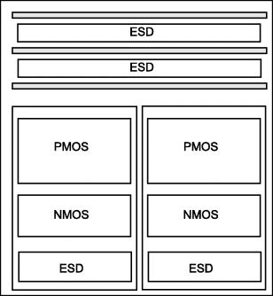
Figure 2.10 is an example of an internal OCD bank architecture with ESD networks. One service module supports the internal OCD bank. This service module contains the ESD VDD-to-VSS power clamp.
Figure 2.10 Internal OCD bank architecture with ESD networks

2.5.2 Array I/O Nibble Architecture
In the ESD design synthesis and floorplanning of semiconductor chips, for performance objectives, off-chip drivers are placed internally to the perimeter of the semiconductor chip. In many applications, it is efficient to have the off-chip drivers in small groupings of four I/O cells placed internally to the semiconductor chip. Figure 2.11 shows an example of a semiconductor chip with internal OCD circuits in a group of four, forming a “nibble.”
Figure 2.11 Array I/O nibble architecture

With the placement of four I/O cells together within the chip perimeter, the following are some of the issues associated with this architecture:
- Local Power Bus: Local power buses must be placed to support the nibble grouping.
- Interconnect Width: Wire width is limited due to internal area constraints.
- Guard Rings: Guard rings must be placed to avoid interaction with adjacent circuitry or other circuit “cores” (e.g., memory, internal logic, de-coupling capacitors).
With a small nibble group, no service module is utilized. As a result, effective ESD design is established. In this example, the ESD solution utilized to provide good ESD protection incorporated the following:
- Sharing of ESD protection between the I/O cells.
- Sharing of ESD protection between two power rails.
With a small nibble group, elements can be shared locally to the nibble group for more compact design and improved ESD protection.
2.5.3 Array I/O Pair Architecture
In some array architectures, instead of the individual external circuits being separated, they are placed in pairs. Figure 2.12 shows an example of an I/O pair placed within dense logic. In the case of array I/O pairs, the configuration can take advantage of sharing of guard rings, and wiring channels. I/O pair configurations can also be suitable for signals where matching is desired between two adjacent signals. I/O pairs are also suitable for differential receiver networks.
Figure 2.12 Array pair I/O architecture
From an ESD perspective, all of the issues associated with array I/O are still present, with the additional issues of I/O to I/O interaction. ESD power clamps must be placed locally and/or embedded in the standard cell. One of the largest issues is the interaction of charge injection from the ESD elements to the adjacent circuitry and cores. Charge injection can disturb the surrounding circuitry or initiate CMOS latchup. Figure 2.13 shows an example of CMOS latchup in the adjacent circuitry near the array I/O pairs. Latchup was initiated by electron injection into the substrate by the ESD elements within the I/O cell [5].
Figure 2.13 CMOS latchup in array pair I/O architecture
2.5.4 Array I/O – Fully Distributed
In array I/O, the I/O can be arranged in groupings, or fully distributed. In a fully distributed array I/O, the ESD design synthesis must account for the spatial distribution of the I/O standard circuitry (Figure 2.14). The ESD floorplan and issues are as follows:
- Interconnects: Metal interconnect width and via number limitations due to transfer wire width.
- Interconnects: Wire width limitation for performance in high-speed input receivers.
- Ballast Resistor: Automated ballast resistor variations.
- ESD Power Clamp: Placement of ESD power clamps.
- Charge Injection: Injection from ESD elements into adjacent dense logic.
- Latchup: Placement of I/O in dense logic can lead to external latchup [5].
- I/O Footprint: I/O cell aspect ratio may differ from the peripheral I/O standard cell.
Figure 2.15 shows an example of the ESD results from an array I/O semiconductor chip. In this technology generation, with array I/O, the ESD results were limited by the interconnects. The ESD results show two distributions of ESD failures. A Gaussian distribution of failures is observed at approximately 6.2 kV, and a second distribution is observed at 10 kV (e.g., ESD tester limitation) [1, 2]. The first distribution has to do with the failure of the transfer wire metal of the ESD interconnects; the second distribution observes no failures. In the case where there was no transfer wire ESD failure, the bond pad and solder ball are placed directly over the array I/O cell. Hence, in this implementation, the transfer wire is the limitation of the array I/O. In the case of this technology, the metal layer was titanium/aluminum/titanium (Ti/Al/Ti), with a worst case failure of approximately 6000 V HBM. With the technology migration to copper interconnects, the semiconductor chip ESD results increased to 9000 V HBM levels. Since copper (Cu) interconnects have a higher critical current-to-failure, the ESD results increased.
Figure 2.14 Fully distributed array I/O architecture
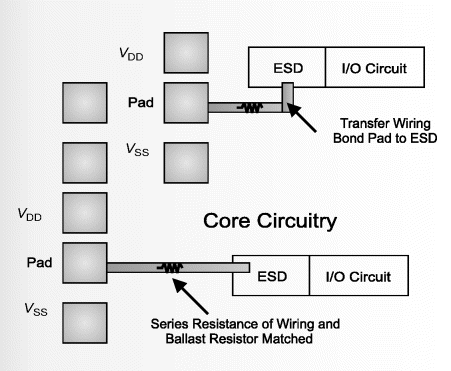
Figure 2.15 ESD results from array I/O architecture

Figure 2.16 shows a picture of the two cases of the solder ball and bond pad over the array I/O cell, and the case when the solder ball and bond pad were not placed over the array I/O cell.
Figure 2.16 ESD failure distribution in array I/O architecture

In the case when the solder ball/bond pad structure was not over the array I/O cell, the failure distribution was associated with the “transfer wire” between the solder ball and the array I/O cell. In this case, the interconnect failed prior to the ESD network silicon failure.
In the case when the solder ball/bond pad structure was over the array I/O cell, the failure distribution was associated with the ESD failure of the ESD network, or the results exceeded the maximum test level of the test system.
Latchup and charge injection is also a concern in this array I/O floorplan [5]. Figure 2.17 shows an example of latchup from an array I/O to dense logic. In the figure, the center region is the ESD diode element. The ESD n-well diode element is surrounded by a guard ring of the array I/O standard cell. Outside the array I/O cell, the surrounding space is CMOS logic. The CMOS logic is a gate array configuration, with no guard ring structures between the n-well and p-well regions. In Figure 2.17, photon emissions are visible in the ESD diode. In the dense logic, photons are evident in the dense logic area. The photons evident in the CMOS logic area are associated with forward biasing and the onset of CMOS latchup.
Figure 2.17 Latchup in array I/O architecture

2.6 ESD Architecture – Dummy Bus Architectures
In semiconductor chip architecture, there are advantages in establishing separate power buses to divert the current from the ESD signal pin network to the ESD power clamps. These “dummy ESD bus” structures play a key role in digital, analog, and RF applications.
2.6.1 ESD Architecture – Dummy VDD Bus
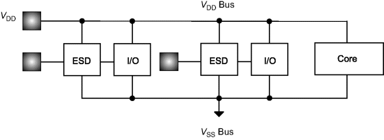
In ESD architecture of a semiconductor chip, a “dummy” VDD bus can be utilized that is distinct from the semiconductor chip power rail. ESD VDD buses separate the ESD discharge from the chip power rail used by the functional circuits. Figure 2.18 shows an example of an ESD dummy VDD bus. The ESD signal pin devices are electrically connected to the ESD dummy VDD bus; this allows the ESD discharge to be directed to the ESD bus instead of the semiconductor VDD power rail. Between the ESD dummy VDD bus and ground is an ESD power clamp element. An additional ESD element can be placed between the VDD power rail and the ESD dummy ground bus, and the semiconductor chip ground, VSS. The usage of the ESD VDD bus has the following ESD design synthesis advantages:
- Full Chip Connections: All ESD signal pins are connected to the independent bus.
- Biasing Voltage: The ESD dummy ground bus can be independently biased to another voltage, decreasing ESD capacitance on the input devices.
- Voltage Tolerance: A lower voltage tolerant level can be used for the ESD power clamp (due to the reduced voltage on the ESD dummy bus).
- Floating Bus: The ESD dummy bus can be left “floating.”
- Design Freedom: ESD dummy bus design (e.g., width) can be set to address ESD concerns, independent of the semiconductor chip power requirements.
2.6.2 ESD Architecture – Dummy Ground (VSS) Bus
In ESD architecture of a semiconductor chip, a “dummy” ground bus can be utilized that is distinct from the semiconductor chip ground. ESD ground buses separate the ESD discharge from the chip substrate ground bus used by the functional circuits. Figure 2.19 shows an example of an ESD dummy ground bus. The ESD signal pin devices are electrically connected to the ESD dummy ground bus; this allows the ESD discharge to be directed to the ESD bus instead of the semiconductor chip substrate. An additional ESD element is placed between the ESD dummy ground bus and the semiconductor chip ground, VSS. The usage of the ESD ground bus has the following ESD design synthesis advantages:
Figure 2.18 ESD dummy VDD bus architecture

- All ESD signal pins are connected to the independent bus.
- The ESD dummy ground bus can be independently biased to another voltage.
- The ESD dummy ground bus can be left “floating.”
- ESD dummy bus design and width can be set to address ESD concerns, independent of the semiconductor chip ground, VSS.
2.7 Native Voltage Power Supply Architecture
Semiconductor chips power supply architecture can be used for the native power supply voltage of the technology. The power supply architecture influences the type of ESD signal pin and the ESD power clamp choice. In the following sections, single and multiple power supply architectures will be discussed.
Figure 2.19 Dummy ESD ground bus architecture

2.7.1 Single Power Supply Architecture
Semiconductor chips can interface with other semiconductor chips or systems with a common power supply voltage. Figure 2.20 shows an example of the semiconductor chip architecture. In the ESD design synthesis, an ESD network is connected to the bond pad. There are two typical architectures:
- The ESD network is connected to the VSS ground rail only.
- The ESD network is connected to the VDD power supply rail and the VSS ground rail.
An example of the ESD signal pin network connected to the VSS ground rail can be a grounded gate n-channel MOSFET (also referred to as GGNMOS). An example of an ESD signal pin network connected to both power rails is a dual diode (also referred to as a double diode).
Figure 2.20 Single power supply architecture with native-voltage interface
To complete the alternative current loop, at least one ESD power clamp is placed in the semiconductor chip. An ESD power clamp is formed between the VDD and the VSS power rails.
2.8 Mixed-Voltage Architecture
In a system, different voltage levels exist for different semiconductor chips that interface with one another. The different voltage levels exist due to both different technology types and technology generations. This becomes an issue for both the interface circuitry, as well as semiconductor chip architectures. As a result, the ESD design synthesis must also address these configurations.
2.8.1 Mixed-Voltage Architecture – Single Power Supply
In a mixed-voltage environment, semiconductor chips must receive or transmit signal levels which are above the native voltage of the technology. To address this, some semiconductor chips have multiple power rails in the design to receive the higher voltage. In a single power supply architecture, only the native voltage of the technology is present on the semiconductor chip.
To address “receiving” or “driving” signal levels above the native voltage power supply, the circuits and ESD networks must have circuitry that is tolerant of the higher voltage levels. The circuit solution for this mixed-voltage interface requirement is addressed as follows:
- Mixed-voltage interface (MVI) OCDs contain series cascode n-channel MOSFET pull-down networks to avoid electrical overstress of the MOSFET [2–4].
- MVI OCDs contain “floating-well” p-channel MOSFET pull-up networks to avoid forward biasing of the p-channel MOSFET (also referred to as n-well-biased off-chip driver) [2, 3, 11–14].
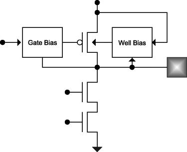
Figure 2.21 shows an example of an n-well-biased OCD network.
Figure 2.21 Mixed-voltage interface n-well-biased OCD
The ESD circuit solution for this mixed-voltage interface requirement is addressed as follows:
- No ESD element is connected to the VDD power supply rail, to avoid forward biasing of the network.
- The MVI ESD network utilizes ESD series diodes to the power supply. ESD diodes consist of p-diffusion-based elements.
- The MVI ESD network contains a “floating-n-well” ESD network to avoid forward biasing of the p + /n-well diode [2].
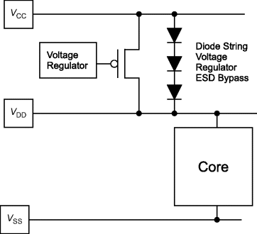
Figures 2.22 and 2.23 show an example of an ESD network used for a 5 V to 3.3 V interface [2–4, 13, 14]. Five p+/n-well diodes are placed between the bond pad and the 3.3 V power supply of the semiconductor chip. The signal pad may switch from 0 to 5 V, yet must interface with the 3.3 V power supply. Five diodes are placed to prevent forward biasing of the ESD network below the worst case power supply conditions. In the first figure, the ESD design layout is shown between the bond pad and the VDD power rail. In the second figure, a circuit schematic containing the ESD “diode string” network is shown.
Figure 2.22 Mixed-voltage interface series diode ESD network layout

Figure 2.23 Mixed-voltage interface series diode ESD network

2.8.2 Mixed-Voltage Architecture – Dual Power Supply
In systems, semiconductor chips are at different application voltages. Semiconductor chips receive signals above the native power supply voltage of the technology. One method to achieve this is to have a semiconductor chip with more than one power supply voltage; the external I/O circuitry is power to the higher power supply voltage, and the internal core circuitry is powered at the native voltage.
Mixed-voltage interfaces also influence the ESD design synthesis and chip architecture. Figure 2.24 shows an example of a semiconductor chip with two power supply voltages. The external peripheral circuits are power to the incoming signal voltages, and the core circuitry is at the native voltage of the technology.
Figure 2.24 Dual power supply architecture

There are multiple ESD architectures that can be established for this environment. The following architectures are examples:
- Sequence-dependent VDD-to-VDD ESD network.
- Sequence-independent VDD-to-VDD ESD network.
- ESD VDD-to-VSS power clamps in the peripheral I/O and core chip regions.
In the ESD design synthesis, a first architecture is to have an ESD network between the power supply rails. A bi-directional ESD network is placed between the two power supply rails. In semiconductor memory chips, the I/O capacitance is small compared to the core capacitance. In memory chips, to save area, the core capacitance can be used due to its low impedance. Figure 2.25 shows an example of a semiconductor memory chip that uses an ESD network between the power supplies. The ESD signal pin device transfers the charge to the external power rail, which then transfers the charge to the core region of the semiconductor chip. An alternative current loop is established from the bond pad to the core. The advantage of this architecture is that no additional ESD power clamps on the peripheral I/O are required, and the core chip capacitance is utilized. This architecture is suitable for large-memory chips, and microprocessors.
Figure 2.25 Dual power supply architecture with ESD network between the two VDD power supply rails
In another ESD design synthesis, ESD VDD-to-VSS power clamps are placed in the internal and external power domains. In this architecture, no ESD network is used between the V′DD and VDD power supply rails. Figure 2.26 shows an example of this architecture. The ESD signal pin device transfers the charge to the external power rail, which then transfers the charge to the peripheral ground rail of the semiconductor chip. In addition, there is an ESD network placed in the ground path (V′SS to VSS). The advantage of this architecture is that no ESD element exists between the two power domains. This avoids concerns over power sequencing, and noise injection into the core circuitry. This implementation requires two different ESD VDD-to-VSS power clamps, due to the voltage tolerance of the internal circuits and external circuits.
Figure 2.26 Dual power supply architecture with peripheral I/O and core ESD power clamp network

In a mixed-signal environment, semiconductor chips can include both digital and analog domains. For mixed-signal CMOS semiconductor chips, both the analog and digital circuitry are MOSFET device elements. For a BiCMOS technology, the digital and analog sectors can contain both CMOS and bipolar transistors.
In a semiconductor chip with bipolar transistors, the architecture of the semiconductor chip may have a VCC power supply, a VSS substrate ground power supply, and a negative-biased VEE power rail. In this three-rail architecture, the ESD power clamps can have different topologies.
2.9.1 Mixed-Signal Architecture – Bipolar
In a mixed-signal environment, or pure analog applications, bipolar transistors are utilized. In a semiconductor chip with bipolar transistors, the architecture of the semiconductor chip may have a VCC power supply, a VSS substrate ground power supply, and a negative-biased VEE power rail. In this three-rail architecture, the ESD power clamps can have different topologies.
In this architecture, the ESD design synthesis has a few options:
- ESD bipolar power clamps between VCC and VSS, and second ESD power clamp between VSS and VEE.
- ESD bipolar power clamps between VCC and VSS, and second ESD power clamp between VCC and VEE.
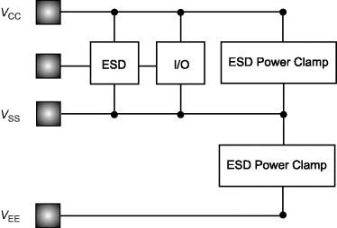
Figure 2.27 shows an example of the power supply architecture. In Figure 2.27, the ESD power clamps are stacked between the VCC and VSS, and a second one between VSS and VEE. In this architecture, the same ESD bipolar power clamp can be used for both cases.
Figure 2.27 Mixed-signal architecture – bipolar ESD power clamps in a stacked fashion. ESD power clamps are between VCC and VSS, and between VSS and VEE
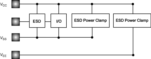
In Figure 2.28, the ESD power clamps are stacked between the VCC and VSS, and a second one between VCC and VEE. In this architecture, the voltage tolerance across the ESD power clamps requires different bipolar transistors with higher breakdown voltages, or elements that are in series cascode within the ESD power clamp.
Figure 2.28 Mixed-signal architecture – bipolar ESD power clamps from VCC to VSS, and from VCC to VEE
2.9.2 Mixed-Signal Architecture – CMOS
Mixed-signal semiconductor chips can be formed with a CMOS technology. In a mixed-signal chip with CMOS technology, the architecture is typically the same power supply voltage, with different power domains established for each chip function domain. Figure 2.29 is an example of a mixed-signal chip commonly found in the semiconductor industry.
Figure 2.29 Mixed-signal architecture

2.10 Mixed-System Architecture – Digital and Analog CMOS
A common mixed-signal application is a semiconductor chip with digital and analog circuitry. In a mixed-signal (MS) architecture, typically the concern is the influence of the noise from the digital circuitry received at the analog circuitry; as a result, the digital and analog circuitry are separated into different power domains.
2.10.1 Digital and Analog CMOS Architecture
In a MS architecture, the digital and analog circuitry are separated into different power domains. Figure 2.30 shows an example of a semiconductor chip with a digital and analog domain. To avoid ESD failures in a MS semiconductor chip, ESD protection networks are placed between the analog ground (AVSS) and the digital ground (VSS). Typical architectures contain a separate ESD power clamp in each domain. An ESD power clamp exists in the digital domain, between VDD and VSS, and a second ESD power clamp exists in the analog domain, between analog VDD (AVDD) and analog ground (AVSS).
Figure 2.30 Mixed-signal architecture – digital and analog with DVSS-to-AVSS ESD network

Alternative architectures are as follows:
- VDD-to-AVDD ESD Network: ESD network between the digital power rail (VDD) and the analog power rail (AVDD) (Figure 2.31).
Figure 2.31 Mixed-signal architecture – digital and analog with DVDD-to-AVDD ESD network

- VDD-to-AVSS ESD Network: ESD network between the digital power rail (VDD) and the analog power rail (AVSS) (Figure 2.32).
Figure 2.32 Mixed-signal architecture – digital and analog with cross-domain ESD network

2.10.2 Digital and Analog Floorplan – Placement of Analog Circuits
In analog design, many considerations are taken to provide good matching and non-uniform characteristics. Analog circuits avoid variations associated with process variations, temperature field, to mechanical stress. Many analog solutions introduce common centroid design practices to improve the matching. On a global level, analog circuits avoid placement next to digital and power domains. Additionally, analog circuits are not placed in the corners of a semiconductor die to wafer warpage, which can lead to mechanical stress variations of the devices.
Figure 2.33 shows an example of a semiconductor die, highlighting the regions where the analog circuits can not be placed [21–23]. Analog circuits can not be placed in the corners of a semiconductor die. For analog ESD design co-synthesis, the corners of the semiconductor die are ideal for ESD power clamps where the space is free to be utilized (Figure 2.34). For pure analog designs, or mixed-signal chips with digital and analog design, this is ideal for allowance of the ESD power clamps.
Figure 2.33 Analog circuit layout restrictions

Figure 2.34 Mixed-signal digital–analog ESD co-synthesis – placement of analog circuits and ESD power clamps

For analog design only, all four corners can be used for the analog power domain (e.g., AVDD to AVSS). Four ESD power clamps can be placed between the two power rails in a periphery design, using the area of the corners where analog circuitry is not allowed to be placed.
For mixed-signal designs, two of the corners can used for ESD power clamps for the digital domain (e.g., digital VDD (DVDD) and digital ground (DVSS)); and the other two corners can be used for the analog power domain ESD power clamps (e.g., AVDD and AVSS). In this architecture, “breaker cells” between the two power domains using ground to ground cells (AVSS to VSS) can be utilized. These breaker cells can be placed in the peripheral architecture design. It is typical in these designs that the digital circuits are separated from the analog domains to avoid digital noise from influencing the analog circuitry. Figure 2.34 shows the digital–analog ESD co-synthesis architecture.
2.11 Mixed-Signal Architecture – Digital, Analog, and RF Architecture
In a MS architecture, the digital, analog, and RF circuitry are separated into different power domains [21–24, 30–32]. Figure 2.35 shows an example of a semiconductor chip with a digital, analog, and RF power domain. To avoid ESD failures in a MS semiconductor chip, ESD protection networks are placed between the analog ground (AVSS), the digital ground (VSS), and the RF ground. Typical architectures contain a separate ESD power clamp in each domain. An ESD power clamp exists in the digital domain, between VDD and VSS, and a second ESD power clamp exists in the analog domain, between analog VDD (AVDD) and analog ground (AVSS), and a third ESD power clamp is between RF VDD (RFVDD or RFVCC) and RF ground (RFVSS or RFVEE). In these mixed-signal chips, the RF application voltage is typically higher than the analog and digital application voltage.
Figure 2.35 Mixed-signal architecture – digital, analog, and RF architecture
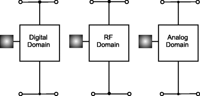
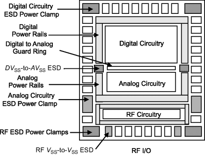
Figure 2.36 shows an example of a floorplan for a mixed-signal chip with RF, analog, and digital circuitry [31]. To separate the analog circuitry from the digital noise, separate power rail domains exist. Additionally, a guard ring “moat” separates the two domains to produce a larger distance through the substrate region. The RF sector is separated on the lower sector of the chip floorplan. The RF circuitry is surrounded by layers of metal, forming a “faraday cage” to isolate the RF signals. The faraday cage is formed by stacking the metal layers, and passing the signals through the breaks in the faraday cage. ESD network power clamps are placed in the digital, analog, and RF domains between their power and ground rails. In addition, VSS to VSS ESD networks are placed to interconnect the ground rails. The VSS to VSS networks use series diode ESD elements, where the number of elements in series is a function of the allowed capacitive coupling between the digital, analog, and RF sectors.
Figure 2.36 Placement and mixed-signal architecture – digital, analog, and RF architecture
2.12 Summary and Closing Comments
In this chapter, the discussion has focused on ESD architecture and floorplan concepts. The chapter focused on “peripheral I/O” and “array I/O” architectures, and how they influence the placement of the various elements for the whole-chip design integration. The chapter also focused on native-voltage, mixed-voltage, and mixed-signal chip integration.
In Chapter 3, the discussion continues to address issues associated with full-chip ESD design synthesis. Chapter 3 focuses on the interconnects and power grid layout and design itself. The chapter will address interconnect robustness, interconnect failure, and key metrics in the whole-chip ESD design synthesis.
Problems
2.1. A chip is formed with I/O and bond pads on the periphery. Draw a semiconductor chip that has dimensions w and l. Assume the bond pads for the circuits are wBP and lBP, with spacing wsp and lsp between bond pads. Assuming the bond pads are on the perimeter, what is the maximum number of bond pads that can be placed on the semiconductor chip? Generalize an equation for the number of bond pads and the chip size relationship. Draw a picture of the chip with the bond pads and spaces. What is the area loss on the corners?
2.2. A chip is formed with I/O and bond pads in an array. Draw a semiconductor chip that has dimensions w and l. Assume the bond pads for the circuits are wBP and lBP, with spacing wsp and lsp between bond pads. Assuming the bond pads are in a mosaic array, what is the maximum number of bond pads that can be placed on the semiconductor chip? Generalize an equation for the number of bond pads and the chip size relationship. Draw a picture of the chip with the bond pads and spaces. If the ESD device for each bond pad is as large as the bond pad, what is the percentage of chip area needed for ESD protection?
2.3. In Problem 1, if the ESD device for each bond pad is 50% as large as the bond pad, what is the percentage of chip area needed for ESD protection?
2.4. Assume, in Problem 1, ESD power clamps are placed in the corners only. What is the area loss in this case?
2.5. Assume, in Problem 1, a VSS power pin is added for every M bond pads, how many power pins can be placed?
2.6. Assume, in Problem 1, a VSS power pin is added for every M bond pads, and a VDD power pin is added for every N bond pads. What is the number of non-power I/O (e.g., signal pins) and number of bond pads for power? Assume an ESD network is placed for each bond pad, and each VSS and VDD pin, what is the total area utilized for ESD protection? Assume the ESD device is a percentage of the bond pad area (parameterize it as a variable p).
2.7. Assume a semiconductor chip has an analog and digital core in Problem 1. Assume there are four power rails, VDD, AVDD, VSS, and AVSS. As in Problem 1, assume a VSS power pin is added for every M bond pads, and a VDD power pin is added for every N bond pads. What is the number of non-power I/O (e.g., signal pins) and number of bond pads for power? Assume an ESD network is placed for each bond pad, and each VSS and VDD pin, what is the total area utilized for ESD protection? Assume the ESD device is a percentage of the bond pad area (parameterize it as a variable p).
2.8. Assume a semiconductor chip has an analog, digital, and RF core in Problem 1. Assume there are six power rails, RFVCC, RFVEE, VDD, AVDD, VSS, and AVSS. As in Problem 1, assume a VSS power pin is added for every M bond pads, and a VDD power pin is added for every N bond pads. What is the number of non-power I/O (e.g., signal pins) and number of bond pads for power? Assume an ESD network is placed for each bond pad, and each VSS and VDD pin, what is the total area utilized for ESD protection? Assume the ESD device is a percentage of the bond pad area (parameterize it as a variable p).
2.9. Assume a semiconductor chip has an analog, digital, and a smart power core in Problem 1. Assume there are six power rails, PVDD, PVSS, VDD, AVDD, VSS, and AVSS. As in Problem 1, assume a VSS power pin is added for every M bond pads, and a VDD power pin is added for every N bond pads. What is the number of non-power I/O (e.g., signal pins) and number of bond pads for power? Assume an ESD network is placed for each bond pad, and each VSS and VDD pin, what is the total area utilized for ESD protection? Assume the ESD device is a percentage of the bond pad area (parameterize it as a variable p). Derive the relationship where the three chip sectors are not equal areas. Define a parameter for the ratio of the areas.
2.10. As in Problem 9, smart power pins require more than one bond pad for signal pins. Assume that the smart power pins require 2× pins per signal, and 4× the ESD network size, how does the relationship change?
1. S. Voldman. ESD: Physics and Devices. Chichester, UK: John Wiley and Sons, Ltd., 2004.
2. S. Voldman. ESD: Circuits and Devices. Chichester, UK: John Wiley and Sons, Ltd., 2005.
3. S. Voldman. ESD: Circuits and Devices. Beijing, China: Publishing House of Electronic Industry (PHEI); 2008.
4. S. Dabral, and T. J. Maloney. Basic ESD and I/O Design. Chichester, UK: John Wiley and Sons, Ltd., 1998.
5. S. Voldman. Latchup. Chichester, UK: John Wiley and Sons, Ltd., 2006.
6. S. Voldman. ESD: Failure Mechanisms and Models. Chichester, UK: John Wiley and Sons, Ltd., 2009.
7. R. Merrill and E. Issaq. ESD design methodology. Proceedings of the Electrical Overstress/Electrostatic Discharge (EOS/ESD) Symposium, 1993; 233– 237.
8. S. Dabral, R. Aslett, and T. Maloney. Designing on-chip power supply coupling diodes for ESD protection and noise immunity, Proceedings of the Electrical Overstress/Electrostatic Discharge (EOS/ESD) Symposium, 1993; 239– 249.
9. S. Dabral, R. Aslett, and T. Maloney, Core clamps for low voltage technologies. Proceedings of the Electrical Overstress/Electrostatic Discharge (EOS/ESD) Symposium, 1994; 141– 149.
10. E. Adler, J. DeBrosse, S. Geissler, S. Holmes, M. Jaffe, J. Johnson, C. Koburger, J. Lasky, B. Lloyd, G. Miles, J. Nakos, W. Noble, and S. Voldman. The evolution of IBM CMOS DRAM technology. IBM Journal of Research and Development, Vol. 39, 1/2., Jan./March 1995; 167–188.
11. S. Voldman V. Gross, M. Hargrove, J. Never, J. Slinkman, M. O'Boyle, T. Scott, and J. Delecki, Shallow trench isolation (STI) double-diode electrostatic discharge (ESD) circuit and interaction with DRAM Circuitry, Proceedings of the Electrical Overstress/Electrostatic Discharge (EOS/ESD) Symposium, 1992; 277– 288.
12. S. Voldman. ESD protection in a mixed voltage interface and multi-rail disconnected power grid environment in 0.5 and 0.25 μm channel length CMOS technologies, Proceedings of the Electrical Overstress/Electrostatic Discharge (EOS/ESD) Symposium, 1994; 125– 134.
13. S. Voldman and G. Gerosa. Mixed voltage interface ESD protection circuits for advanced microprocessors in shallow trench and LOCOS isolation CMOS technology, International Electron Device Meeting (IEDM) Technical Digest, December 1994; 811– 815.
14. S. Voldman, G. Gerosa, V. Gross, N. Dickson, S. Furkay, and J. Slinkman. Analysis of snubber clamped diode string mixed voltage interface ESD protection networks for advanced microprocessors. Proceedings of the Electrical Overstress/Electrostatic Discharge (EOS/ESD) Symposium, 1995; 43– 62.
15. S. Voldman. The impact of MOSFET technology evolution and scaling on electrostatic discharge protection. Journal of Microelectronics Reliability, 1998, 38; 1649–1668.
16. S. Voldman. The impact of technology evolution and scaling on electrostatic discharge (ESD) protection in high-pin-count high-performance microprocessors. Proceedings of the International Solid State Circuits Conference (ISSCC), Session 21, WA 21.4, February 1999; 366– 367.
17. S. Voldman. CMOS-on-SOI ESD protection networks. Proceedings of the Electrical Overstress/Electrostatic Discharge (EOS/ESD) Symposium, 1996; 291– 301;
and Journal of Electrostatics, 1998; 42; 333–350.
18. S. Voldman. Electrostatic discharge (ESD) protection in silicon-on-insulator (SOI) CMOS technology with aluminum and copper interconnects in advanced microprocessor semiconductor chips. Proceedings of the Electrical Overstress/Electrostatic Discharge (EOS/ESD) Symposium, 1999; 105– 115.
19. S. Voldman, D. Hui, L. Warriner, D. Young, R. Williams, J. Howard, V. Gross, W. Rausch, E. Leobangdung, M. Sherony, N. Rohrer, C. Akrout, F. Assaderaghi, and G. Shahidi. Electrostatic discharge protection in silicon-on-insulator technology. Proceedings of the IEEE International Silicon on Insulator (SOI) Conference, 1999; 68– 72.
20. P. A. Juliano, and W. Anderson. ESD protection design challenges for a high pin-count Alpha microprocessor in a 0.13 μm CMOS SOI technology. Proceedings of the Electrical Overstress/Electrostatic Discharge (EOS/ESD) Symposium, 2003; 59– 69.
21. P. Gray, Hurst, Lewis, and Meyer. Analysis and Design of Analog Integrated Circuits. Fifth Edition. New York: John Wiley and Sons, Inc., 2009.
22. W.M.C. Sansen. Analog Design Essentials. Amsterdam: Springer, 2006.
23. A. Hastings. The Art of Analog Layout. Second Edition. New Jersey: Pearson Prentice Hall, 2006.
24. V. Vashchenko and A. Shibkov. ESD Design in Analog Circuits. New York: Springer, 2010.
25. S. K. Ghandi. Semiconductor Power Devices, New York: John Wiley and Sons, Inc., 1977.
26. P. Antognetti. Power Integrated Circuits: Physics, Design, and Applications. New York: McGraw-Hill, 1986.
27. B. J. Baliga. High Voltage Integrated Circuits. New York: IEEE Press, 1988.
28. B. J. Baliga. Modern Power Devices. New York: John Wiley and Sons, Inc. 1987.
29. V. Vashchenko, M. Ter Beek, W. Kindt, P. Hopper. ESD protection of high voltage tolerant pins in low voltage BiCMOS processes. Proceedings of the Bipolar Circuits Technology Meeting (BCTM), 2004; 277– 280.
30. S. Voldman. The state of the art of electrostatic discharge protection: Physics, technology, circuits, designs, simulation and scaling. Invited Talk, Bipolar/BiCMOS Circuits and Technology Meeting Symposium, 1998; 19–31.
31. S. Voldman. ESD: RF Circuits and Technology. Chichester, UK: John Wiley and Sons, Ltd., 2006.
32. R. Singh, D. Harame, and M. Oprysko, Silicon Germanium: Technology, Modeling and Design, New York: John Wiley and Sons, Inc., 2004.