
8
Fourth Order Interleaved Boost Converter With PID, Type II and Type III Controllers for Smart Grid Applications
Saurav S.* and Arnab Ghosh
Department of Electrical Engineering, National Institute of Technology Rourkela, Rourkela, India
Abstract
Switched mode power converters are an important component in interfacing renewable energy sources to smart grids and microgrids. The voltage obtained from power conversion is usually full of ripples. In order to minimize the ripple in the output, certain topological developments are made. Increasing the energy storage elements and interleaving them for 180° phase shift reduces the ripple in the circuit. This is made possible by controlling the converters using Type II and III controllers and the results are compared with PID controller. The performance is analyzed and compared in Simulink environment. Transient and steady state analysis is done for better understanding of the system.
Keywords: Interleaved fourth order boost converter, higher order converters, Type II and III controllers, PID controller, smart grid interface, k-factor approach
8.1 Introduction
In the evolving age of cyber physical systems, several technologies and algorithms have been developed for automation where human effort is minimum. One example of such system is the smart grids. Smart grids are evolving faster to accommodate the growing energy demands. These grids are well-equipped with systems which can select the power sources considering various real time loses in the system. In order to fully utilize the power from different sources, these equipments must reduce the losses to minimum. Smart grids and microgrids play a major part in renewable energy applications. These systems are employed to harness the energy obtained from natural sources such as sun, wind, etc. [1]. In order to effectively utilize the power generated from these sources, an efficient dc-dc power converter has to be designed [2–4]. These dc–dc converters are used depending on the application like increasing or reducing the obtained voltage depending on the load, MPPT (Maximum Power Point Tracking) [5] tracking, regulated DC voltage and battery charging applications.
There are several innumerable topologies which exist in the current research literatures which are developed to address this problem [6]. Many topologies including the higher order topologies and the tristate converters which are used to address the research problems. Higher order converters are basically required for reducing the ripple in the circuit, as it has more energy storing elements than normal dc–dc power converters [7, 8]. Interleaved converters have also been researched extensively and their construction is in such a way that the energy storing elements and the switches are parallel to one another [9]. So basically, interleaved converter is also a form of higher order converter. This is done specially to reduce the ripples as well as the size and loses of ripples in the output filter. There are other topological modifications such as tristate boost converters which also has an extra mode and degree mode of freedom which have been proven to remove the non-minimum phase in the boost converter [10]. In this chapter the discussion is about higher order boost converters. Just like other boost converters the interleaved boost converter also has a pole in the right half of the s-plane [11]. As a result of this non-minimum phase, the closed loop bandwidth is restricted [12]. The restriction of closed loop bandwidth leads to slower response of the system. The order of the converter is more and when PID controller is used, difficulty lies in controlling the output voltage during line and load regulation and also amidst parametric uncertainties. So, the PID controller can be tuned to Type II or Type III controller based on the applications [13].
The discussion in this chapter is entitled to two phases interleaved [14–17] fourth order boost converter [18] each of which is fourth order. The characteristics of the interleaved converters apply here as well. The two phases are 180° out of phase with each other. This converter is modeled and controlled using Type II and III controllers [19–25]. The results obtained are compared with PID controller and with each other and a conclusion is derived from the comparison.
Here in this chapter, state space modeling which is more convenient is used to model the power converter, and it is derived in Sections 2.1 and 2.2. The state space averaging techniques and the small signal analysis are discussed in Sections 2.3 and 2.4 respectively through which the transfer functions of the plant are derived. After modeling is done, various controllers suited for the converters are analyzed and discussed in Section 8.3. The responses of the designed power converter are analyzed and the result obtained from the simulation is compared for the two types of controllers designed in Section 8.4. Section 8.5 is the conclusion derived from this virtual simulation conducted.
8.2 Modeling of Fourth Order Interleaved Boost Converter
8.2.1 Introduction to the Topology
The fourth order Interleaved Boost converter (FIBC) consists of two Fourth order boost converters which are connected in parallel with respect to energy storing elements and switches as shown in Figure 8.1. The total number of energies storing elements are seven, of which there are four inductors (L1, L2, L3, L4) and three capacitors (C1, C2, C3). There are also two controlled switches which are basically MOSFETs (S1 and S2) and two uncontrolled switches which are the diodes (D1 and D2). When comparing it with regular Fourth order Boost converter in Figure 8.2, it has three extra energy storing elements in the middle with the exception of an output capacitor. Thus, it can be said as a parallel combination of two Fourth order boost converters except the source voltage (Vg), load (R) and output capacitor (C3) are unique.
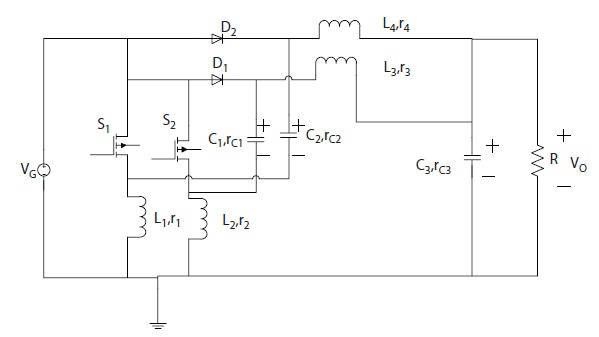
Figure 8.1 General configuration of fourth order interleaved boost converter.

Figure 8.2 General configuration of fourth order boost converter.
8.2.2 Modeling of FIBC
There are four modes of operation when the Fourth order interleaved circuit diagram is considered. It has two controlled switches (in this case MOSFET S1 and S2) and two uncontrolled switches (the two diodes D1 and D2). The different modes and the corresponding steady state equations are discussed for every mode of operation.
8.2.2.1 Mode 1 Operation (0 to d1Ts)
In this mode the MOSFET S1 is On, the diode D1 is Off, the MOSFET S2 is On and the diode D2 is On. The equivalent circuit diagram following this mode of operation is shown below:
By applying KVL and KCL in Figure 8.3 we get the following equations,

Figure 8.3 Mode 1 operation of FIBC.


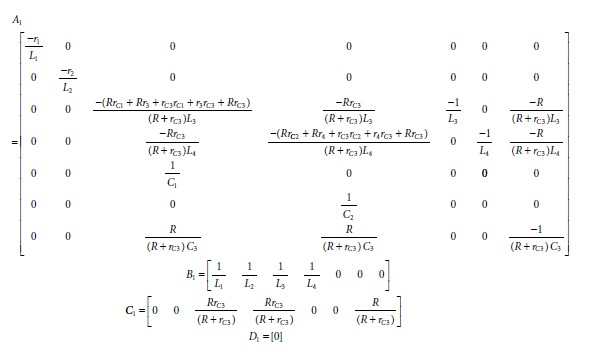
The above equations (Eqs. (8.1)–(8.7)) obtained from mode 1 are converted into state space form and the representation is given below:
Here,
8.2.2.2 Mode 2 Operation (d1Ts to d2Ts)
In this mode the MOSFET S1 is On, the diode D1 is OFF, the MOSFET S2 is OFF and the diode D2 is On. The equivalent circuit diagram following this mode of operation is shown below:
By applying KVL and KCL in Figure 8.4 we get the following equations,


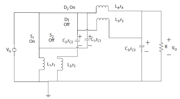
Figure 8.4 Mode 2 operation of FIBC.


The above equations (Eqs. (8.10)–(8.16)) obtained from mode 1 are converted into state space form and the representation is given below:

Here,
8.2.2.3 Mode 3 Operation (d2Ts to d3Ts)
This mode is exactly the same as mode 1. The equivalent circuit diagram following this mode of operation is shown below:
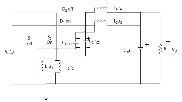
Figure 8.5 Mode 3 operation of FIBC.
By applying KVL and KCL in Figure 8.5 we get the following equations,

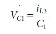
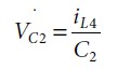
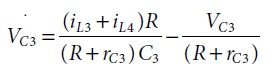
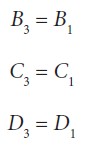
The above equations (Eqs. (8.19)–(8.24)) obtained from mode 3 are converted into state space form and the representation is given below:
Here,
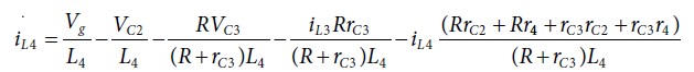
8.2.2.4 Mode 4 Operation (d3Ts to Ts)
In this mode the MOSFET S1 is Off, the diode D1 is On, the MOSFET S2 is On and the diode D2 is Off. The equivalent circuit diagram following this mode of operation is shown below:
By applying KVL and KCL in Figure 8.6 we get the following equations,

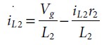
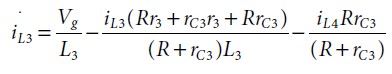

Figure 8.6 Mode 4 operation of FIBC.

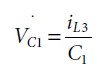
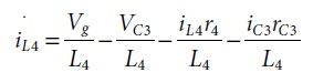
The above equations (Eqs. (8.28)–(8.34)) obtained from mode 2 are converted into state space form and the representation is given below:
Here,

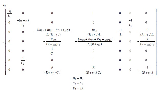
8.2.3 Averaging of the Model
State space averaging is done to ensure that the four modes of operation happen during a single clock cycle. The four state space matrices in Eqs. (8.8–8.9), (8.17–8.18), (8.26–8.27) and (8.35–8.36) are averaged according the formula given below in Eqs. (8.37–8.42).
Where


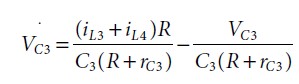
8.2.4 Small Signal Analysis
The transfer functions are obtained by adding perturbations to the instantaneous values of state variables and control variable.
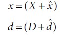
where D, X are the steady state values and ![]() and
and ![]() are the perturbations (small signal).
are the perturbations (small signal).
After substituting the small signal values in the above generated state space equations, we get,
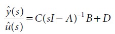
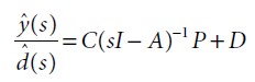
Input to output transfer function (I2O) is obtained by substituting ![]() and Control to output transfer function (C2O) is obtained by substituting
and Control to output transfer function (C2O) is obtained by substituting ![]() respectively in Eq. (8.43).
respectively in Eq. (8.43).
The transfer functions are obtained as given below;
I2O is given by:
C2O is given by:
Where,
| Parameter | Value |
| Vg | 20 V |
| R | 20 Ω |
| VO | 50 V |
| r1, L1, r2, L2 | 0.055 Ω, 250 μH |
| r3, L3, r4, L4 | 0.035 Ω, 110 μH |
| rC1, rC2, C1, C2 | 0.1 Ω, 22 μF |
| rC3, C3 | 0.1 Ω, 220 μF |
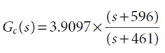
Table 8.1 represents the values for converter parameters to be substituted in Eqs. (8.44) and (8.45) to form a transfer function. The switching frequency is assumed to be 80 KHz. By substituting these values, we get the following transfer function.
Input to Output Transfer function:

Control to output Transfer function:
From Figure 8.7 we can see that the root locus depicts the presence of zeros and poles in the C2O transfer function. As observed from the figure, there exists a zero in the RHP of the imaginary axis (s-plane). This represents the non-minimum behavior of the transfer function of boost converters. This right half plane zero exist only in the C2O transfer function and not in the I2O transfer function as seen from Figure 8.8. This non minimum behavior can be observed from the bode plot in Figure 8.9. Around the cut off frequency, the non-minimum nature can be observed from the bode diagram.
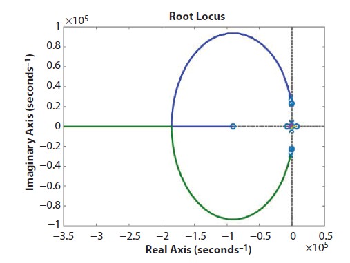
Figure 8.7 Root locus of Gvd.
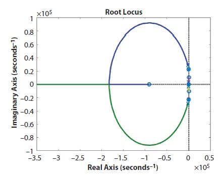
Figure 8.8 Root locus of Gvg.
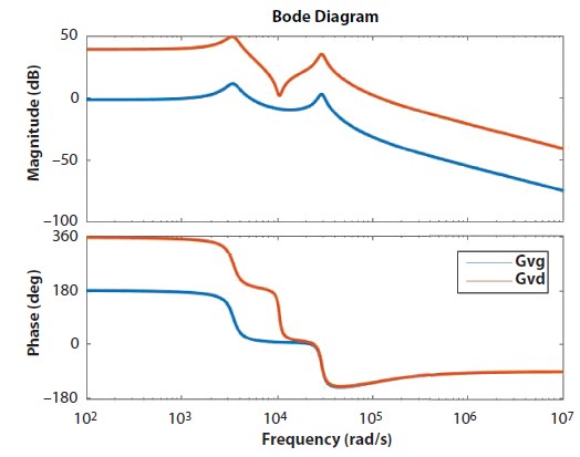
Figure 8.9 Comparison of Bode plots of the two transfer function of FIBC.
8.3 Controller Design for FIBC
8.3.1 PID Controller
This controller is taken as a reference for the comparison of the Type II and III controllers. This is the most popular controller used in the industry and the comparison of this controller with the rest of the discussed topics provides a reasonable explanation. The PID controller consists of three terms Proportional, Integral and derivative parts. These are represented in the form of an expression in frequency domain (Eq. (8.47)). It is given by
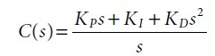

By using Ziegler–Nicholas tuning method we get the values for the three PID parameters in Eq. (8.47) and the transfer function is given by,

8.3.2 Type II Controller
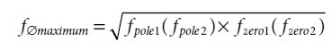
This controller is nothing but a lead circuit combined with an integrator. The main focus of this controller is that it gives a higher phase boost (Ømax) of up to 90°. In this regard, the controller is designed in such a way as to obtain a desired phase margin of around 60°. The general representation of a type II controller is given in Eq. (8.48).
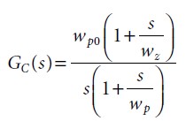
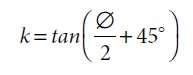
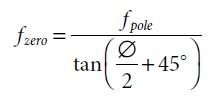
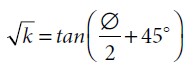
Where wp, wz are the pole and zero locations of this controller. Tuning of the controller parameter is a very important criteria for the design of any controller. Here k-factor approach is used for the tuning of the controller parameters. Here k is the ratio of pole location to zero location. This value of k is defined according to the frequency domain design criteria. In this design example, a phase margin of about 60° is considered for this controller. The amount of phase boost to achieve a phase margin of 60° is the required phase boost (Ø) in this design. K is given by Eq. (8.49).
The Pole location is given by Eq. (8.50).

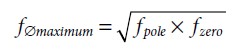
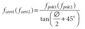
The value of Ø is noted from the Figure 8.9. The frequency at which the Ø is calculated is the cut-off frequency. Correspondingly, the frequency of maximum phase is given by Eq. (8.51).
The zero frequency location is given by Eq. (8.52).
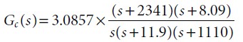
After finding the pole and zero location, the transfer function becomes,
8.3.3 Type III Controller
This controller is nothing but the combination of an integrator and lead-lead circuit. The main focus of this controller is that it gives a maximum phase boost (Ømax) of 180°. In this regard, the controller is designed in such a way as to achieve a phase margin of around 90°. The general representation of a Type III controller is given by Eq. (8.53)
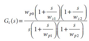
Where wz1, wz2, wp1, and wp2 are the zeros and poles of this controller’s transfer function respectively. Similar to Type II controller, here also the same approach is used for tuning the controller parameter for this controller’s transfer function. K is defined in a similar way for this controller also. It is given in Eq. (8.54).
Where Ø is the phase boost required to maintain the desired phase margin.
The pole location is given by Eq. (8.55).

The value of Ø is noted from the magnitude-frequency plots of the converter’s transfer function. The corresponding frequency of phase boost (Ø) is called the cut off frequency (fcut − off). The value of frequency of max. phase boost (Ømax) is given by Eq. (8.56).
From the above calculated values, we can arrive at the zero location frequency is given from Eq. (8.57).
After finding the pole and zero location of this controller, the transfer function is given by,
8.4 Computational Results
The system performance of FIBC is realized with the three controllers and the results are compared with conventional PID controllers for better analysis. The simulation is done in the MATLAB environment. The results obtained are satisfactory when compared with ordinary Fourth Order Boost converter when operated with the same controllers.
The step response of FIBC along with Type II controller is plotted in the Figure 8.10. The bode diagram as well as the root locus plot of the system is depicted in Figures 8.11 and 8.12. From these plots, it is inferred that the converter with Type II controller settles in 7 msec. The rise time is found to be 4.2 msec. This results in the faster convergence of the system when compared with PID controller. The PID controller’s settling time for the same converter is approximately 10 msec and the rise time is approximately 5 msec. The step response involving PID controller tuned with the classical design formula is shown in Figure 8.13.
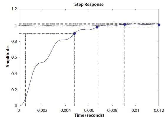
Figure 8.10 Response of FIBC with Type II controller.
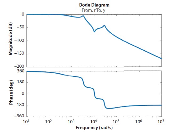
Figure 8.11 Bode diagram of FIBC with Type II controller.

Figure 8.12 Root locus of FIBC with Type II controller.
It can be inferred from the above plots that the Type III controller (Figure 8.14) settles faster when compared with the other two controllers. The settling time is observed to be less than 5 msec and the rise time is 2.5 msec. Thus, we can conclude that the Type III controller exhibits faster response when compared with all other controllers discussed here (Figure 8.15). This FIBC is in fact, faster than the ordinary Fourth order Boost converter without interleaving operation (Figure 8.16). The comparison of the transient response of the three controllers in closed loop with the converter is plotted in the Figure 8.17. The comparison of the closed loop bode response with different controllers are also shown in the Figure 8.18. From this plot we can observe the phase boost achieved in closed loop system when compared with the uncompensated system.

Figure 8.13 Response of FIBC with PID controller.

Figure 8.14 FIBC with Type III controller.

Figure 8.15 FIBC with Type III controller-magnitude and phase plot.
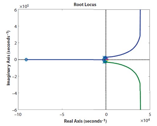
Figure 8.16 Root locus of FIBC with Type III controller.
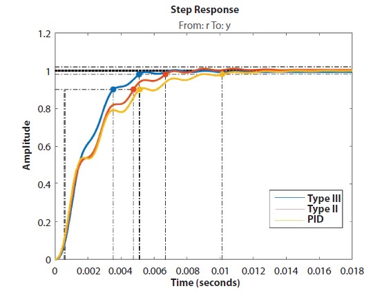
Figure 8.17 Comparison of the different controllers in closed loop operation.
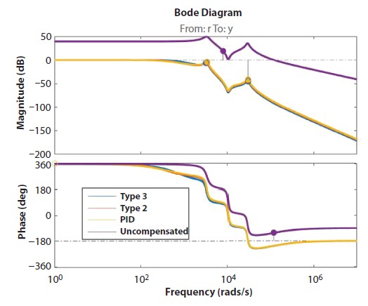
Figure 8.18 Comparison of the bode response of different controllers in closed loop.
Table 8.2 Comparison of different controllers in closed loop performance.
| Parameter | PID controller | Type-II controller | Type-III controller |
| Rise time | 0.0052 s | 0.004 s | 0.0025 s |
| Settling time | 0.01 s | 0.007 s | 0.0048 s |
| Maximum peak overshoot | 0% | 0% | 0% |
| Gain margin | 9.1 dB | 12.5dB | 9.79 dB |
| Phase margin | 59° | 62.8° | 80° |
| Steady state error | 0.0 | 0.0 | 0.0 |
From Table 8.2, it is noted that the Type III controller performs well with FIBC. It is worth noted that this performance reflects both in frequency domain as well as time domain.
Comparison of the Different Controller’s Responses During Steady State
As we can observe from Figures 8.19 and 8.20 reference tracking is carried by the addition or subtraction of 50% of the desired output voltage. This is done to ensure that the designed controller has good tracking tolerance despite the system being designed for a specific voltage. Here, it is observed from the above graphs that the system involving Type III controller settles faster when compared with the other two controllers even though the changes are very small.
Line regulation is one of the important criteria in analyzing the robustness of the system. It is done by checking the tolerance of the changes in input voltage by at least 10% of the actual input voltage. It can be observed from Figure 8.21 that the three controllers behave almost identical when this change is applied. The oscillation occurs for few milliseconds and it eventually settles down. This lies within the approvable range in the literatures.
In Figure 8.22 changes in the load in terms of load voltage are observed. This is identical to changing the load at the output in simulation environment. Here, a part of the voltage (−50%) is added to the existing load voltage. The output is seen disturbed for a few milliseconds before it settles down to the reference value. It is evident from this Figure that the oscillations in Type III settles faster when compared with the Type II and PID controllers.
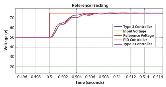
Figure 8.19 Comparison of the three different controllers when 50% of reference voltage is added.
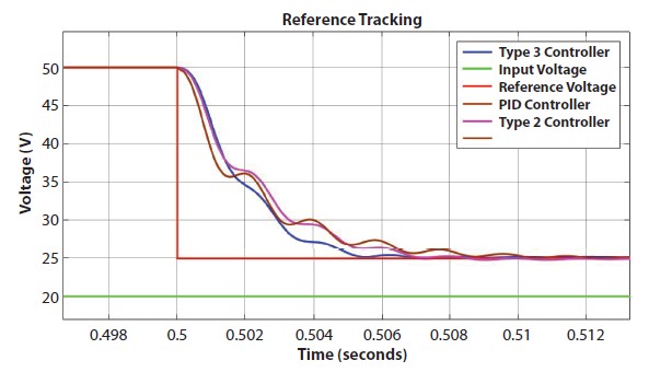
Figure 8.20 Comparison of the three different controllers when 50% of reference voltage is subtracted.
Figure 8.23 depicts the ripple in the output of this converter. Its value is approximately 0.3 V. The percentage ripple is 0.6%. This is very less when compared with the normal fourth order boost converter which is close to 1.5%. This percentage of ripple changes as the duty ratio is varied. The percentage of ripple varies inversely with the duty ratio.

Figure 8.21 Comparison of the changes in 10% of input voltage for different controllers in closed loop.
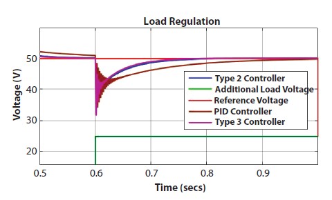
Figure 8.22 Comparison of the load regulation by adding additional load voltage in the circuit (−50% of load voltage).
8.5 Conclusion
It is observed that the discussed converter is stable and agrees with the reference voltage. It is clear from the graphs that converter is underdamped initially and after approximately 7 msec it settles down. in the case of Type II controller and in approximately 5 msec for a Type III controller. The rise time also reduces considerably when compared with PID and Type II controller. The simulation results are according to the desired value and is improved in terms of quicker response and source fluctuations. The steady state responses of the simulation results proves that the controller is stable and robust as well. The reference tracking and regulation subjected to disturbances does not alter the nature of the output voltage although certain fluctuations are present at the time of impact after which it settles down to the desired value. Thus, this converter can be effectively used in smart grids for compensation in the supply voltage due to any irregularities in the supply voltage. FIBC can be used in smart grids or microgrids to aide in harnessing the potential of renewable energy with minimum losses.
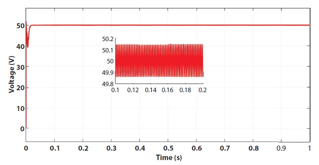
Figure 8.23 Ripple in the output of FIBC.
References
1. Liu, X. and Su, B., Microgrids—An integration of renewable energy technologies, in: 2008 China International Conference on Electricity Distribution, IEEE, pp. 1–7, 2008.
2. Erickson, R.W. and Maksimovic, D., Fundamentals of Power Electronics, Springer Science & Business Media, USA, 2007.
3. Ogata, K., Modern Control Engineering, Prentice Hall, USA, 2010.
4. Sivakumar, S., Jagabar Sathik, M., Manoj, P.S., Sundararajan, G., An assessment on performance of DC–DC converters for renewable energy applications. Renew. Sust. Energ. Rev., 58, 1475–1485, 2016.
5. Hohm, D.P. and Ropp, M., Comparative study of maximum power point tracking algorithms. Prog. Photovolt.: Res. Appl., 11, 1, 47–62, 2003.
6. Vijayakumari, A., Warner, B.R., Devarajan, N., Topologies and control of grid connected power converters, in: 2014 International Conference on Circuits, Power and Computing Technologies [ICCPCT-2014], IEEE, pp. 401–410, 2014.
7. Veerachary, M. and Saxena, A.R., Design of robust digital stabilizing controller for fourth-order boost DC–DC converter: A quantitative feedback theory approach. IEEE Trans. Ind. Electron., 59, 2, 952–963, 2011.
8. Babu, C.S. and Veerachary, M., Predictive valley current control for two inductor boost converter, in: Proceedings of the IEEE International Symposium on Industrial Electronics, 2005. ISIE 2005, vol. 2, IEEE, pp. 727–731, 2005.
9. Banerjee, S., Ghosh, A., Rana, N., An improved interleaved boost converter with PSO-based optimal type-III controller. IEEE J. Emerg. Sel. Top. Power Electron., 5, 1, 323–337, 2016.
10. Rana, N., Kumar, M., Ghosh, A., Banerjee, S., A novel interleaved tri-state boost converter with lower ripple and improved dynamic response. IEEE Trans. Ind. Electron., 65, 7, 5456–5465, 2017.
11. De Nardo, A., Femia, N., Nicolo, M., Petrone, G., Spagnuolo, G., Power stage design of fourth-order DC–DC converters by means of principal components analysis. IEEE Trans. Power Electron., 23, 6, 2867–2877, 2008.
12. Hoagg, J.B. and Bernstein, D.S., Nonminimum-phase zeros-much to do about nothing-classical control-revisited part II. IEEE Control Syst. Mag., 27, 3, 45–57, 2007.
13. Papadopoulos, K.G., Papastefanaki, E.N., Margaris, N.I., Optimal tuning of PID controllers for type-III control loops, in: 2011 19th Mediterranean Conference on Control & Automation (MED), IEEE, pp. 1295–1300, 2011.
14. Rahavi, J.S.A., Kanagapriya, T., Seyezhai, R., Design and analysis of interleaved boost converter for renewable energy source, in: 2012 International Conference on Computing, Electronics and Electrical Technologies (ICCEET), IEEE, pp. 447–451, 2012.
15. Kumar, G.V.B. and Palanisamy, K., Interleaved Boost Converter for Renewable Energy Application with Energy Storage System, in: 2019 IEEE 1st International Conference on Energy, Systems and Information Processing (ICESIP), IEEE, pp. 1–5, 2019.
16. Henn, G.A.L., Silva, R.N.A.L., Praca, P.P., Barreto, L.H.S.C., Oliveira, D.S., Interleaved-boost converter with high voltage gain. IEEE Trans. Power Electron., 25, 11, 2753–2761, 2010.
17. Kamtip, S. and Bhumkittipich, K., Design and analysis of interleaved boost converter for renewable energy applications, Rajamangala University of Technology Thanyaburi, 2011.
18. Saurav, S. and Ghosh, A., Design and Analysis of PID, Type II and Type III controllers for Fourth Order Boost Converter, in: 2021 7th International Conference on Electrical Energy Systems (ICEES), IEEE, pp. 323–328, 2021.
19. Ghosh, A., Banerjee, S., Sarkar, M.K., Dutta, P., Design and implementation of type-II and type-III controller for DC–DC switched-mode boost converter by using K-factor approach and optimisation techniques. IET Power Electron., 9, 5, 938–950, 2016.
20. Ghosh, A. and Banerjee, S., A comparative performance study of a closed-loop boost converter with classical and advanced controllers using simulation and real-time experimentation. Int. Trans. Electr. Energy Syst., 30, 10, e12537, 2020.
21. Ghosh, A. and Banerjee, S., A comparison between classical and advanced controllers for a boost converter, in: 2018 IEEE International Conference on Power Electronics, Drives and Energy Systems (PEDES), IEEE, pp. 1–6, 2018.
22. Ghosh, A. and Banerjee, S., Control of Switched-Mode Boost Converter by using classical and optimized Type controllers. J. Control Eng. Appl. Inform., 17, 4, 114–125, 2015.
23. Ghosh, A. and Banerjee, S., Design and implementation of Type-II compensator in DC-DC switch-mode step-up power supply, in: Proceedings of the 2015 Third International Conference on Computer, Communication, Control and Information Technology (C3IT), IEEE, pp. 1–5, 2015.
24. Almusaylim, Z.A. and Zaman, N., A review on smart home present state and challenges: linked to context-awareness Internet of Things (IoT). Wirel. Netw., 6, 3193–3204, 2019.
25. Chatterjee, J.M., Kumar, R., Khari, M., Hung, D.T., Le, D.N., Internet of Things based system for Smart Kitchen. Int. J. Eng. Manuf, 8, 4, 2.9, 2018.
- *Corresponding author: [email protected]