
11
Quantum Optical Switches
Surabhi Yadav and Aranya B. Bhattacherjee
Department of Physics, Birla Institute of Technology and Science‐Pilani, Hyderabad Campus, Telangana, India
11.1 Introduction
Enormous data transfer within optical fiber networks has created a global communication revolution that has impacted human life and modern economic activity. High bit rate optical connections have been extended to numerous other networks over the last few decades, from long‐distance transmission networks to short‐distance communications inside buildings [1]. A photonic switch with an ultrashort decay time is one of the main components in establishing a high‐speed optical signal processing device [2]. The high power requirement of photonic to electrical and electrical to photonic conversions inspired the concept of using photonic networks as a substitute for modern electronic switching. Terahertz switching speed is possible with an optical switch that controls light signals directly through another optical beam, with possible restoration times in the pico‐ or femtosecond range. The accessibility of such a system together with the use of low‐dissipation photonic waveguides and fibers could pave the way for a high bit rate, low‐cost optical network over short distances. For efficient all‐optical switching, optical non‐linearity with low power consumption (low photon number) is a necessary prerequisite. Optical non‐linearity at single photon level have been demonstrated in many studies over the years, indicating the possibility of implementing low‐power and high bit rate photonic devices for classical information processing [3]. Solid‐state devices based on a sole quantum dot coupled strongly to a nano/micro optical cavity are potential candidates for such applications. These devices have a limited carbon footprint and are compliant with standard nano‐fabrication procedures.
High difference switching, switching at a high speed, and multi‐wavelength configuration were also achieved using photonic switching based on saturable absorbers fabricated using quantum wells in vertical micro cavities [4]. The use of resonant distributive Bragg reflectors (DBR) structure is one way to reduce the energy loss in optical switches. The use of semiconductor quantum dots within DBR micro cavities for high‐speed optical switching was studied in a recent experiment [5] and theoretical work [6].
The combination of quantum dots and micro cavities allows for an excellent method for studying cavity quantum electrodynamics. The potential of a quantum dot in a mesoscopic cavity to produce non‐linear optical effects motivates us to investigate the opportunity of controlling the photon statistics in these systems for practical applications [7]. Single InAs quantum dot in a GaAs photonic crystal cavity was used to explain electro‐optical switching at the quantum level [8]. In cavity quantum electrodynamics, the device works in the robust/strong coupling regime. The quantum‐confined Stark shift is used to tune the quantum dot by changing the quantum dot frequency [9]. Within nm‐sized clusters, quantum dots have three‐dimensional confined states [10]. In ultrafast photonics, quantum dots have a wide range of applications. Mode‐locked quantum dot lasers and a quantum dot semiconductor saturable absorber mirror have used the ultra‐broad optical range of self‐assembled quantum dots as an absorption saturator [11].
The rapid growth and versatility of opto‐mechanical systems and optomechanics have sparked a lot of interest and study over the last few decades [12]. Cavity optomechanics is a branch of microphysics and quantum optics that studies how electromagnetic field interacts with mechanical systems. Optomechanically induced transparency (OMIT) [13], quantum entanglement [14], quantum synchronization [15], quantum state transfer [16], and optomechanically induced non‐reciprocity [17] are only a few of the recent developments and breakthroughs in quantum optomechanics. As a result, it establishes a strong base for quantum optical communication and quantum information processing.
A high level of nonlinearity occurs between the optical and mechanical modes in optomechanical systems, resulting in optical bistability and multistability. This optical phenomenon has applications in optical switching and memory storage in general [18]. Because of the optomechanical nonlinearity, the bistable behavior exhibits switching actions controlled by adjusting the laser strength, rocking parameter, optomechanical coupling, and QD cavity coupling [19]. Through micro‐mechanical oscillators, a quantum interface can pass the quantum state between different degrees of freedom. Another promising system for implementing quantum switches is a electro‐opto‐mechanical system in which a mechanically compliant DBR/membrane is interacting simultaneously with a microwave as well as an optical cavity [20]. Such a hybrid system has been shown to exhibit tunable optical switching behavior. Also, reversible quantum state transfer between microwave and optical photons is possible with hybrid electro‐optomechanical systems [21].
11.2 Quantum Dot as an Optical Switch
The speed of electronic components in various electronic communication devices limits the capacity of photonic communication systems that can exceed 10 Tb/s due to the high frequency of the optical carrier. Electronic components can be substituted with high‐speed all‐optical signal processing components to overcome these limitations [22]. As switches require an extremely fast response, low laser power consumption, and the ability to accommodate multiple channels, photonic switches for future optical networks are looking to be a suitable candidate for 2DPC (two‐dimensional photonic crystal) applications [23].
Ultrafast semiconductor devices based on quantum dots (QDs) can operate at speeds of 10 to 100 GHz or even higher. The following are some of the significant benefits of QD‐based devices:
- Low power consumption, as demonstrated by low‐threshold QD laser and QD‐based optical switches.
- Enhanced thermal stability, as shown by temperature‐insensitive lasers and QD semiconductor optical amplifiers (SOAs) with ultralow noise and no pattern effect.
- Wide bandwidth, as shown by SOA and QD‐based solid‐state saturable absorber mirrors, and also used as incoherent broadband sources.
These three benefits provide a strong foundation for QD‐based devices to be obviously appealing for use in future less power‐consuming optical networks, also known as the “Green internet” on a macro scale, which involve low‐power, low‐noise, and broadband operation. An optical switch with ultra‐short delay time is one of the main systems for establishing a high‐speed optical network. The excitation power needed to enter the nonlinear operation regime for most optical materials is relatively high, limiting system efficiency (the well‐known “power/speed trade‐off”). The necessary energy per pulse for the fabrication of chip‐based photonic networks is estimated to be less than one PJ/bit. Owing to the small volume and density of states similar to that of atoms, semiconductor nanostructures like QDs should be able to meet such a system requirement. As a result, quantum dot‐based structures can produce high optical non‐linearity while consuming very little energy. For the characterization of all‐optical switches, two other parameters, differential reflectivity (or transmission) and switching time, are especially important. These parameters refer to two major QD limitations, namely the degree of the optical nonlinearity and the speed of the carrier dynamics, in the case of QD switches. Due to their dispersed distribution in both actual and frequency space, the interaction length and effective cross‐section of self‐assembled QDs are extremely limited. In order to generate high optical nonlinearity and, as a result, high differential reflectivity in practical devices, the light‐QD interaction must be improved. Integrating QDs with either two‐dimensional waveguides made out of photonic crystal or vertical cavities will partially solve the problem of light’s poor interaction with QDs. The photonic crystal waveguide of μm scale with hundreds of photonic air holes results in a system with a wide surface area and potentially high cost. Optical switches fabricated using QD embedded in vertical cavities will be a good option in terms of power efficiency. One‐dimensional photonic crystals, which are also known as vertical cavity, improve the optical mode‐QD interaction while preserving the low power consumption advantage. In comparison to Quantum Well (QW) devices, QD interband transitions are not inherently easy. The existence of such slow recombination rates can limit the device’s switching efficiency. Non‐radiative channels may be introduced into QW products using methods such as impurity doping combined with low‐temperature processing. These techniques, on the other hand, minimize absorption intensity and hence optical nonlinearity. Such techniques could be used in QDs, but defect‐related methods must be controlled with extreme caution due to the low absorption values. The existence of discrete energy levels in QDs, fortunately, provides another diverting procedure for manipulating switching dynamics.
11.2.1 Vertical Cavities
The function of a QD optical switch using a Febry–Perot cavity is illustrated schematically in Figure 11.1. Two distributed Bragg reflector (DBR) mirrors, each with several pairs of alternating high and low refractive index layers, make up the semiconductor‐based optical cavity. According to the output direction, the two DBR mirrors are called back and front mirrors. Each independent layer of the DBR mirror has a thickness of ![]() . Here n is the refractive index of the DBR layer and k is the operation wavelength. The cavity area between two layers of DBR has a thickness L =
. Here n is the refractive index of the DBR layer and k is the operation wavelength. The cavity area between two layers of DBR has a thickness L = ![]() (m is an integer), referred as the k cavity [11].
(m is an integer), referred as the k cavity [11].


Figure 11.1 All optical switch using QDs in a vertical photonic crystal cavity.
where the reflectivity of the back and front mirrors are RB and RF respectively and Λ is the collective absorption in QDs. As laser light is pumped into the optical cavity, the light reflected by one mirror can be ultimately canceled by the reflection from the second mirror in the cavity mode, as long as the two reflected beam are out of phase. This mechanism is used in both QW/QD and bulk materials in vertical‐geometry optical switches. The relationship between front and back reflectivity explains the so‐called “zero reflectivity state”.
A photonic bandgap area with high reflectivity close to 100% is seen. When the zero reflectivity requirement is met, the light beam will completely penetrate the cavity without reflection in the resonant cavity mode. The absorption of quantum dots saturates when heavy pumping of laser power occurs at the resonant cavity mode. This disrupts the device’s zero reflectivity state and causes it to switch modes. A large differential reflectivity between the operation states with and in the absence of pumping is needed for efficient switching.
For several years, the limitations imposed by physical dimensions of optical switches have been a source of contention. Keyes and Armstrong [24] presented the first significant discussion of this subject in the late 1960s, concluding that optical power utilization will be a major issue preventing the use of optical devices. This contention persisted until the 1980s when technology based on QW and optical bistability were discovered. Using the quantum‐confined stark effect (QCSE), a high degree of optical nonlinearity was demonstrated in semiconductors, leading to a series of active realizations of photonic logic device.
There are certain important properties of optical microcavities that is taken into account while designing and fabricating these structures. The quality factor (Q‐FACTOR) defined as the ratio of a resonant cavity frequency ωc to the Full Width at Half Maxima (FWHM) of cavity mode ![]() ,
,
The Q factor is a parameter which determines the rate at which optical energy decays from the cavity.
The finesse Fc of the cavity is
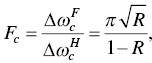
where ![]() is free spectral range or, in other words, the frequency seperation between the successive longitudinal optical modes of the microcavity. R is the total power reflectivity. The on‐resonance optical intensity enhancement factor is defined as:
is free spectral range or, in other words, the frequency seperation between the successive longitudinal optical modes of the microcavity. R is the total power reflectivity. The on‐resonance optical intensity enhancement factor is defined as:

In a microcavity, this enhancement is non‐uniform and spatially localized. One can couple a two‐level system such as a QD directly to this localized and enhanced optical field to harness strong coupling and optical nonlinear interaction.
11.2.2 Power Density
The coupled oscillator model widely used in cavity quantum electrodynamics (CQED) research can theoretically reflect the QD cavity structure. Figure 11.2 shows a two‐level system (QD) in a photonic crystal cavity with an interaction strength g, cavity mode decay rate κ and carrier relaxation time, T1. The mechanism is assumed to operate in the weak coupling regime, i.e. g << κ. The semi‐classical method using Maxwell–Bloch equations yields the absorption and phase nonlinearity of QDs.

Here, σ is the off‐diagonal component of the density matrix, δ is the population inversion term, Δ is the detuning of the optical field from resonance, g is the QD‐field coupling strength and T2 is the dipole phasing time.
We present a brief quantum optical analysis of a QD cavity system coupled strongly to show optical switching effect. The study is valid for any single‐mode cavity and excludes any photonic crystal‐specific charateristics. The Hamiltonian H describing the quantum dynamics of the system of a QD embedded in a photonic crystal cavity is [3]
where wo and wq are the resonance frequencies of the cavity and the QD respectively, a(σ) is the lowering operator for the cavity mode (Quantum dot). σ is equal to |g >< e| with |g > and < e| being the ground and excited state of the QD respectively. The strength of interaction between the QD and the optical cavity mode is g = Ω/2, where Ω is the vacuum Rabi splitting. This Hamiltonian can be diagonalized to find the system’s eigen‐energies. The bare cavity resonance splits into two resonances due to the QD‐cavity interaction, corresponding to the coupled system’s eigen state, also known as polaritons, in a strongly coupled QD‐cavity system when g > (κ − γ)/2, where κ is the field decay rate and γ is decay rate of the QD. As a result, when the cavity contains a single strongly coupled QD, the transmission of a laser whose frequency is resonant with the frequency of the empty cavity is significantly reduced.
As a function of laser power, normalized cavity output transmission is calculated. The coupled QD‐cavity system’s nonlinear transmission characteristic is depicted in Figure 11.3. This is the switch’s direct current behavior. The split resonance is a result of the QD‐cavity coupling. On changing the detuning around the resonance condition of Δ/g, the output transmission changes between zero transmission (OFF state) to maximum transition (ON state).
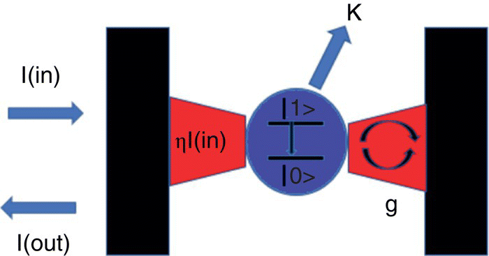
Figure 11.2 Photonic cavity coupled with a QD.
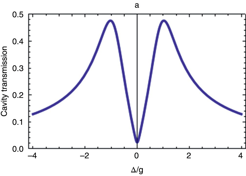
Figure 11.3 The DC transmission characteristics of an all‐optical switch constructed from a strongly coupled QD‐cavity system.
The switching speed of any switch is a critical parameter. One can numerically measure the optical response of the coupled dot‐cavity method to estimate the switching speed. Two pulses drive the coupled device, and complete optical transmission through the cavity is detected. When the two pulses are separated by a significant amount of time, they are transmitted separately via the QD‐cavity device. We assume a steady transmission as a function of time. However, as the pulses get closer in time, they begin to overlap, resulting in a more excellent transmission due to the system’s non‐linearity.
Figure 11.4 depicts a diagram of the planned tunable optical transmission. Two DBR mirrors made of quarter‐wavelength tick alternating layers of different dielectric materials make up the unit. A cavity spacer area, forming a DBR microcavity, separates the two mirrors. The cavity spacer contains QDs which act as saturable absorbers to generate a light intensity‐dependent optical cavity.
Two independent laser signals, an input laser signal and a control laser, are used to activate the switch, as shown in Figure 11.4. The carrier frequency of the two signals is chosen to be the same. The input signal comes in from the top surface of the DBR and is supposed to be of low‐intensity such that the QDs are not saturated. The control signal is strong enough to saturate the QDs, changing the cavity’s absorption. Except for random emission noise, the weak signal and strong control pulses move in orthogonal directions and are entirely distinct and separable. The DBR structure gives rise to low reflectivity since all the light is transmitted at low QD density. The DBR makes uninterrupted transitions from transmitting to highly reflecting as the QD density increases. The increased absorption inside the cavity causes this transition. The reflectivity is affected in two ways by increasing the number of DBR layers. First, the density of QDs needed to change the cavity reflectivity diminishes as the number of QDs increases and second, the maximum reflectivity obtained in the high‐density regime also grows.
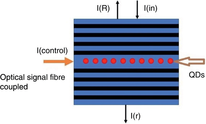
Figure 11.4 DBR‐QD switch.
11.3 Quantum Well as an Optical Switch
For Quantum Wells (QW), conduction band electrons and valence band holes behave as particles with a certain effective mass (me and mh corresponding to that of electron and hole) which is not the same as the free electron/hole mass. According to the “k.p” band theory, me and mh are approximately equal and proportional to the band gap energy.
Quantum wells are an example of a hetero‐structure, which is a structure formed by fusing dissimilar materials, typically in layers, and with the materials being fused right at the level of atoms. Hetero‐structures in general have a wide range of applications. State‐of‐the‐art electronic devices (e.g. resonant tunneling devices, modulation‐doped field‐effect transistors, hetero junction bipolar transistors), optical materials (e.g., wave guides, mirrors, micro resonators), and optoelectronic devices and structures (e.g., laser diodes, photo detectors, quantum wells) all benefit from hetero‐structures. Although hetero‐structures are helpful in electronics, they also play an essential role in many optoelectronic devices (e.g., lasers). Perhaps their most valuable technical feature is that they can be used for many of these electronic, optical, and optoelectronic applications, allowing them to be integrated.
11.3.1 Optical Properties
To comprehend the interband linear optical absorption in quantum wells, we ignore the “excitonic” effects. This is an excellent conceptual first model that describes some of the critical properties. Unlike in bulk semiconductors, excitonic effects in quantum wells are very visible at room temperature and significantly impact device performance. By absorbing a photon, an electron can rise from the valence band to a state in the conduction band having the same momentum (a “vertical” transition). The state in the conduction should have similar momentum because the photon has no momentum on the scale, usually of interest in the semiconductor. In this simple model, we also assume that all such transitions have the same strength, even though they will have dissimilar energies. We have a selection rule corresponding to the direction perpendicular to the layers in quantum wells rather than momentum conservation, as shown in Figure 11.5. The transition is allowed between states with the same quantum number in the conduction and valence bands (to lowest order). The strength of optical absorption is directly proportional to the overlap of the valence and conduction wave functions, resulting in this rule. In quantum wells, holes and electrons are still free to move in a plane parallel to the layers. There are no discrete energy states for holes and electrons; instead, there are “subbands” that begin at the calculated confined state energies. For a particular confined state, the electron can aquire any kinetic energy corresponding to its 2D motion in the QW. Also, it can have any energy which is larger than or equal to the energy of a confined state for that subband.
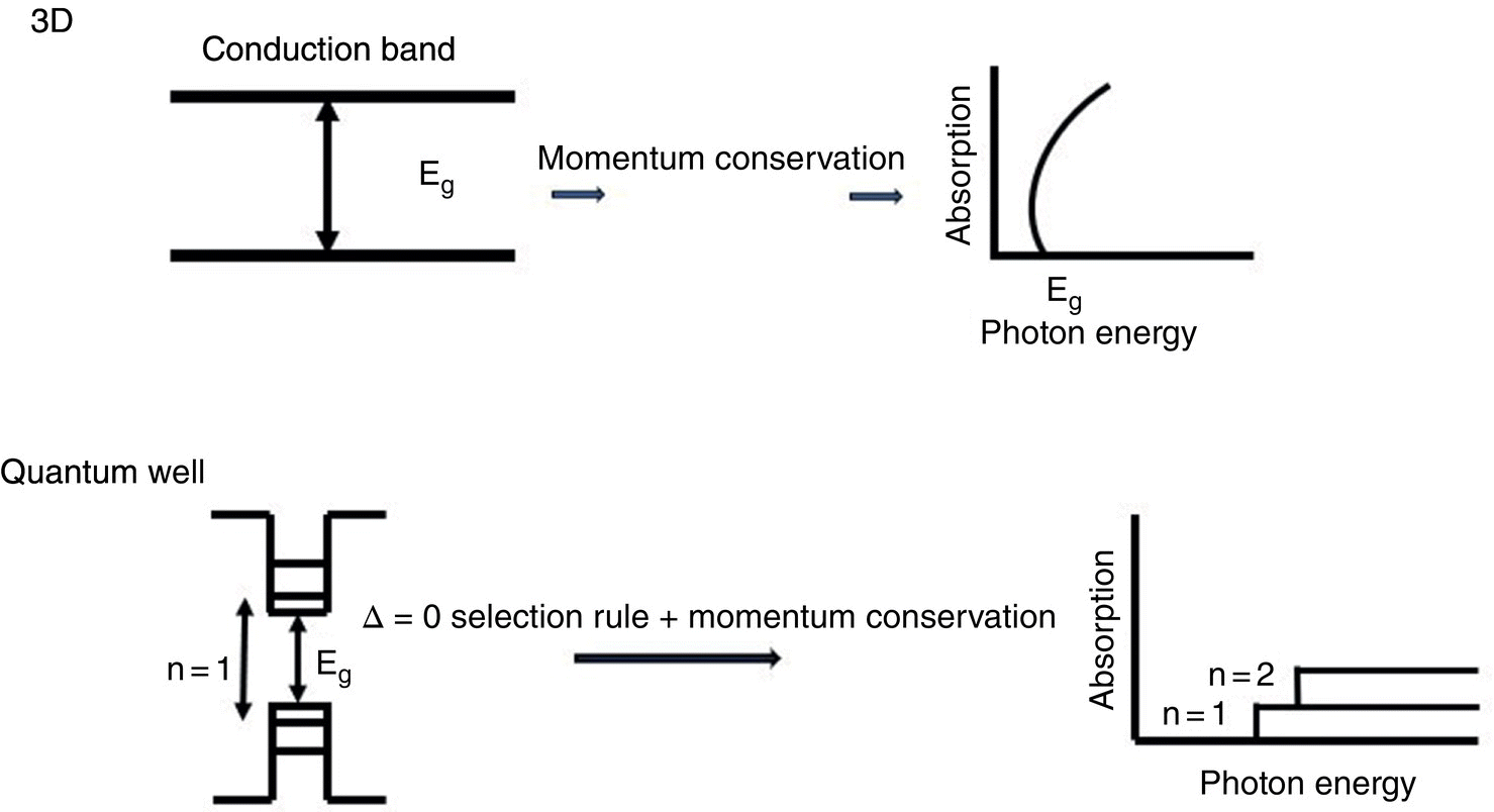
Figure 11.5 Optical absorption in bulk and in QW.
Absorption in the quantum well occurs in step, and particle‐in‐a‐box calculations give the position of these steps correctly. However, there are peaks in the spectra that are not estimated or described by this simple “non‐excitonic” model. These spectral peaks have a significant influence and will be especially noticeable near the band‐gap energy.
We must now introduce the concept of excitons in understanding these peaks (electron‐hole pair). The correct approach is to consider creating an electron‐hole pair rather than raising an electron from the valence band to the conduction band. First, we must analyze and understand the states corresponding to an electron‐hole pair in a crystal. The creation of a particle, the exciton, is used to explain optical absorption. It is critical to understand that we are not lifting an existing hydrogen‐like particle to an excited state, as is done with usual atomic absorption; rather, we are creating the particle. The absorption of electron‐positron pairs in the vacuum is an analogy that could help explain this difference. The quantum well differs from bulk material in two important ways, both of which arise from the quantum well’s confinement as shown in Figure 11.6. When we create an exciton in a 100 Å‐thick quantum well, the exciton shrinks in all three directions.

Figure 11.6 Comparison of bulk and QW exciton sizes and shapes.
Quantum wells can exhibit a wide range of nonlinear optical effects. Only one type of effect, saturation of optical absorption near the band‐gap energy, will be discussed in this section. This set of effects has been extensively studied for various systems and is suitable for applications in laser mode‐locking [25]. In the most basic instance, we direct a laser on the material, causing the associated optical absorption to generate a large population of holes and electrons, resulting in “excitons” or “free carriers”. Absorbing at the peaks corresponding to the exciton generates excitons, whereas absorbing at greater photon energies produces free carriers.
We cannot make two identical excitons in the same spatial region. As we start to create space excitons, we run out of space and as a result, the likelihood of creating more excitons must decrease, as must the optical absorption associated with it. As a result, the exciton absorption line will reach saturation. Screening effects are the second type of mechanism that can alter absorption. When we increase the density of free carriers, the dielectric constant changes, and thus the size of the exciton changes, usually increases. When the exciton size increases, the possibility of finding the hole and electron in the same place is diminished; as a result, the strength of optical absorption also diminishes, resulting in an effect similar to saturation. In quantum wells, the saturation effects corresponding to the exciton peak are very sensitive. A variety of nonlinear optical switching devices have been investigated using them.
11.3.2 Self‐Electro‐Optic‐Effect Devices
The theory behind the self‐electro‐optic effect system (SEED) is to combine a quantum well modulator (or group of photodectors) to create an optically operated system with an optical output (or outputs). Although the conversion from optics to electronics and back is often inefficient and costly, this does not have to be if the devices are well integrated. The quantum well devices can be effectively integrated, allowing innovative optoelectronic units to be created. Such devices open up new avenues for data processing and switching architectures. There are two types of SEEDs: those that only use diodes and those that also use transistors. Figure 11.7 shows the most basic SEED configuration. It exhibits optical bistability and is a “resistor‐biased” SEED (R‐SEED).
A positive feedback system in SEED is responsible for the bistability. Assume that there is not much light shining on the diode at first. The result is a low photocurrent and as a consequence, a low voltage drop around the resistor. Hence, the maximum supply voltage appear across the diode, and the diode absorption is strong. We get more photocurrent as we shine more light on the diode. We now have less voltage across the diode due to the voltage decrease across the resistor, and hence more absorption, and thus more photocurrent. We can switch into a highly absorbing state as a result of this mechanism. Decreasing to a lower power level eventually makes the diode revert to its high‐voltage, low‐transmission state as shown in Figure 11.8.
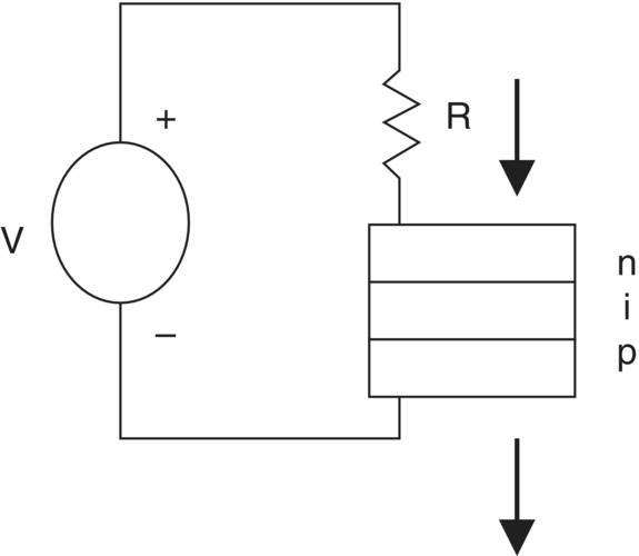
Figure 11.7 Basic SEED configuration.
11.4 Optomechanical Systems as Optical Switch
11.4.1 Optical Nonlinearity
Within the framework of classical optics, optical bistability belongs to a category of non‐linear optical phenomena in which the refractive index of the material through which an intense beam of light is allowed to pass depends on the intensity of the incident light,
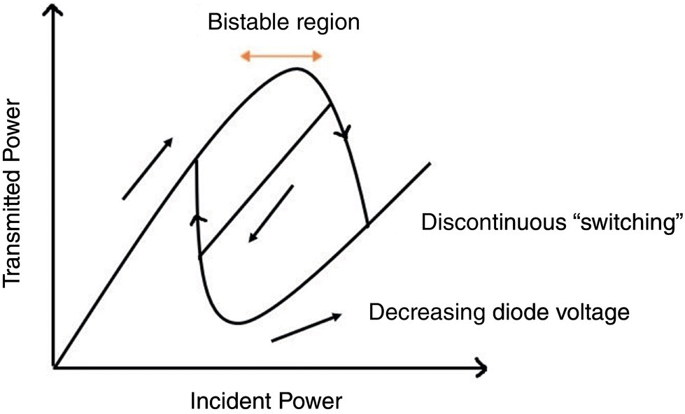
Figure 11.8 Bistable curve for SEED operating as an optical switch.
where n0 is the linear refractive index, n2 is the nonlinear index, and I is the intensity of light. Optical bistability leads to the possibility of designing “all‐optical switches” (also called photonic switching). The nonlinear coefficient n2 depends on the third‐order susceptibility χ(3) as [26]:

where c is the speed of light in vacuum. In optical/photonic switching, the output state of the device depends on the current state of the device. Coherently controlling the system parameters, the device can be made to switch between “high” and “low” state. Optical nonlinearity can also lead to multistability, thus leading to the possibility of a new type of logic beyond binary logic.
Photonic switching in a nonlinear Fabry–Pérot etalon has been described earlier [27]. The transmitted intensity as a function of incident intensity in a nonlinear Fabry–Pérot etalon exhibits a hysteresis loop (optical switching) as shown in Figure 11.9.
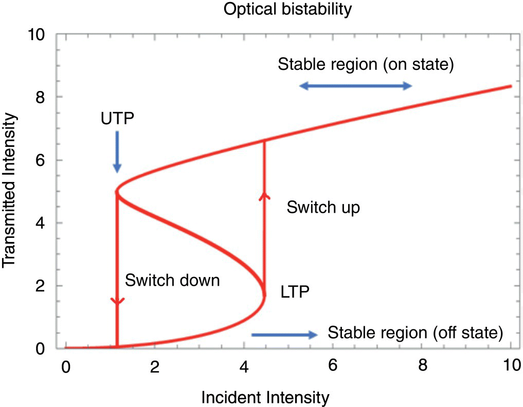
Figure 11.9 Schematic representation of a system showing optical bistability.
Figure 11.9 shows the hysteresis loop that the transmitted intensity follows as the incident intensity is gradually increased or decreased. Initially if transmitted intensity (I0) is on the lower stable region (off state) and as incident intensity (Ii) increases past its lower turning point (LTP), I0 switches upto the upper stable region (on state). As long as I0 remains larger than its value at LTP, I0 is given by the upper stable region solution. Now as we gradually decrease Ii below the upper turning point (UTP), I0 switches down to the initial lower stable region (off state.)
Photonic switching devices have applications in optical computing and experimental efforts are targeted towards realizing novel materials which can lead to optical devices based on optical bistability. Experimental progress in nano‐materials and photonic crystals has led to a revival of photonic devices [28].
11.4.2 Hybrid Optomechanics
An optical field is used in optomechanical systems to measure and control the dynamics of the mechanical resonator. The optical field is typically confined within a cavity, which allows for resonant enhancement of field strength and mechanical displacement sensitivity. Radiation pressure is a scattering force caused by light reflection, which has momentum associated with it. Optical gradient forces result from the spatial variation of optical intensity. The bistability of an optomechanical cavity is the result of the static effect of radiation pressure. A shift in frequency and modified dissipation of the mechanical resonator are the dynamic effects of radiation pressure combined with a finite cavity lifetime.
A Fabry–Pérot optical cavity in which one of the mirrors is mechanically compliant is the most basic optomechanical system in which optical pressure provides the optomechanical coupling as shown in Figure 11.10. The mechanical resonator’s motion changes the length of the optical cavity and thus the resonance frequency of the cavity. The coupling is calculated by determining the relationship between the cavity resonance frequency and the mechanical component’s displacement.
Let us consider the most basic optomechanical system as depicted in Figure 11.10.
The Hamiltonian of the system is given as
where ![]() and
and ![]() are the annihilation operators for the cavity mode and the mechanical mode, respectively. Ωc and Ωm are the optical and mechanical frequency respectively. The length of the cavity L, is shifted by the mechanical oscillator’s motion, with L = L − q, where q is the mechanical oscillator’s displacement away from its equilibrium location. Since the cavity length is not fixed due to one of the mirrors being movable, the cavity frequency is dependent on the length of the cavity Ωc(q). The mode frequency of the cavity is
are the annihilation operators for the cavity mode and the mechanical mode, respectively. Ωc and Ωm are the optical and mechanical frequency respectively. The length of the cavity L, is shifted by the mechanical oscillator’s motion, with L = L − q, where q is the mechanical oscillator’s displacement away from its equilibrium location. Since the cavity length is not fixed due to one of the mirrors being movable, the cavity frequency is dependent on the length of the cavity Ωc(q). The mode frequency of the cavity is

where  is the longitudinal optical mode wavelength with mode number j. Therefore, the Hamiltonian of the system is rewritten as
where g0 = Gxzp is the single photon optomechanical coupling, G is the cavity mode frequency shift caused by the mechanical resonator’s zero‐point motion xzp and the last term is defined as the interaction part of the Hamiltonian (remember ![]() ; note that now
; note that now ![]() is a position operator). The Hamiltonian shows that a movable mirror’s interaction with the radiation field is essentially a nonlinear mechanism involving three operators.
is a position operator). The Hamiltonian shows that a movable mirror’s interaction with the radiation field is essentially a nonlinear mechanism involving three operators.
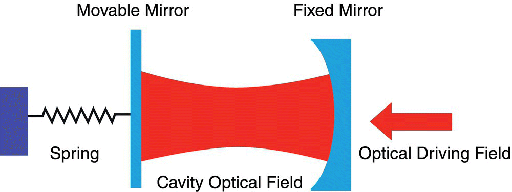
Figure 11.10 Cavity optomechanical system consists of an optical cavity formed of two high‐reflectivity mirrors. One of the mirrors is fixed while other is movable.
We rotate the Hamiltonian of the above equation in the frame of reference of the pump frequency ΩL, as a result of which we get the following Hamiltonian:
Here, Δ is the detuning between the optical cavity and the incident laser frequency as
The open system dynamics of a cavity optomechanical system are described by the Langevin equation of motion.

where  is the position and
 ![]() is the momentum quadrature of the mechanical oscillator while κ and Γ are the decay rates of the optical cavity and mechanical oscillator respectively.
is the momentum quadrature of the mechanical oscillator while κ and Γ are the decay rates of the optical cavity and mechanical oscillator respectively.
Consider that the mechanical oscillator is guided incoherently by its bath (< Pin >= 0) and describes the cavity’s coherent amplitude ![]() , proportional to the mean optical cavity occupancy N introduced by coherent driving by N = |α|2. Hence,
, proportional to the mean optical cavity occupancy N introduced by coherent driving by N = |α|2. Hence,

These equations show a nonlinear coupling between the mechanical oscillator and the optical field, resulting in a wide variety of classical behaviour, including parametric instability regimes marked by exponential growth in mechanical oscillation amplitude. The steady states of α and Q are represented as αs and Qs respectively and are derived as


Figure 11.11 Intracavity photon number as a function of cavity detuning. The figure demonstrates optical bistability due to the inherent optomechanical nonlinearity present in the system.
Equations (17) and (18) represent two coupled equations giving rise to nonlinear effect observed as optical bistability which is shown in Figure 11.11.
Bistability is a common occurrence in many nonlinear systems. The nonlinearity of the equations of motion indicates that such effects can be observed through optomechanical coupling. Experiments have shown that optical bistability can exist in semiconductor microcavities. In these systems, several mechanisms could lead to bistable behavior. One possible mechanism is to introduce nonlinearity into the system by increasing exciton density, which results in exciton‐exciton scattering. Bleaching the Rabi splitting is another method for achieving bistable behavior [29]. Optomechanical bistability can be understood better due to a competition between the mechanical restoring force and the radiation pressure force, which is highest at the cavity resonance. The optomechanical coupling can squeeze the cavity mode, and this effect is maximal near the bistable regime. It has also been observed that quantum entanglement is maximum at the bistability threshold under certain conditions [30].
A hybrid system is made up of an optomechanical cavity and a second optical cavity containing an ensemble of ultra‐cold atoms that serves as feedback to the first cavity. The bistable response of the intracavity field in the optomechanical cavity can be coherently tuned by varying the frequency of the single control laser, which drives the cavity‐field detuning in the optomechanical cavity and the atom‐field detuning in the atomic cavity. Compared to a single‐cavity optomechanical system, this allows for more flexibility in tuning bistability [31]. The optical spring effect generated due to optomechanical coupling between the cavity field and the oscillator is indicated by the multistability of the displacement of a mechanical oscillator coupled to a cavity field. In non‐zero detuning, multistability is a sign of dynamical back‐action, which causes the mechanical oscillator to heat or cool. This is because multistable behavior indicates a change in the oscillator’s decay rate and resonance frequency. Multistability is also an essential factor in the design of all‐optical switches, logic gates, and memory devices. The photon tunneling rate between two coupled cavities controls optomechanical bistability and multistability, which occurs at low input power levels [32].

Figure 11.12 A schematic figure of an Electro‐opto mechanical system.
11.4.3 Electro‐opto Mechanics
Figure 11.12 shows a hybrid electro‐optomechanical system (EMOS). It consists of a mechanical resonator (MR) capacitively coupled to the microwave field of a superconducting microwave cavity (MC) on one side and an optical cavity on the other (OC). By tuning the various interactions, the system can exhibit optical switching behaviour at low input power levels [21]. The system’s controllable bistable behaviour demonstrates that it can be used as an all‐optical switch, logic gates, and memory device for quantum information processing with low energy power input.
The fact that silicon nitride membranes have remarkable optical and mechanical properties was a key development discovery. The oscillations of the silicon nitride membrane interact with the electromagnetic field confined in the cavity when placed between the two mirrors that form a high‐quality factor Fabry–Pérot cavity. State‐of‐the‐art experiments use metallic membranes to create low‐loss capacitors that naturally couple membrane vibrations to electrical signals at microwave frequencies. Cryogenic temperatures are required for these experiments in order to minimize Johnson noise at microwave frequencies and to create low energy‐loss superconducting circuits. The integration of the two electromagnetic resonators is the most difficult aspect of building an electro‐optomechanical system.
The optical cavity must function at low temperatures required by the microwave circuit. The microwave circuit must operate near the Fabry–Pérot cavity, where light from the cavity may couple with the microwave circuit. High‐frequency light absorbed by a superconducting microwave circuit, in particular, can harm its performance. Photons with energies larger than the superconducting gap can separate Cooper pairs into their electrons. The frequency converter is built with a physically large silicon nitride membrane. The superconducting microwave circuit and optical cavity can couple to spatially distant portions of the silicon nitride membrane. Standard photolithographic techniques are used to fabricate a silicon nitride membrane fixed by a silicon frame. A portion of the membrane is also covered in niobium, used in the superconducting circuit. Figure 11.13 shows the schematic of the electro‐opto mechanical system fabricated and used for microwave to optical frequency conversion [33].
11.5 Conclusion and Future Outlook
We have discussed the current technological progress of optical switching systems based on semiconductor nanostructures. Quantum photonic devices can be designed by focusing and guiding light into semiconductor nanostructures, which play an essential role in future generation power‐efficient optical networks. The present development of optical switches shows excellent potential to meet future optical communication systems requirements between electronic chips or within chips. A hybrid optomechanical system is capable of storing and transferring information, thus forming a part of a quantum information processing unit. All‐optical switches have received much interest because they can overcome the speed limitation of electric switches. A solid‐state‐based optomechanical system in the presence of an additional second‐order nonlinearity is found to be highly tunable and can be used to implement low‐power switching devices. The mean‐field optical bistability of a hybrid electro‐optomechanical system in the presence of a qubit displays optical switching characteristics which can be tuned to consume low input power.
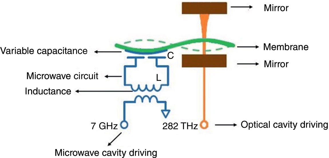
Figure 11.13 Schematic of a optical‐to‐microwave frequency converter.
Source: Modified from Andrews [33].
Bibliography
- 1 C.‐Y. Jin and O. Wada. Photonic switching devices based on semiconductor nano‐structures. Journal of Physics D: Applied Physics, 47 (13):133001, 2014. doi: 10.1088/0022‐3727/47/13/133001.
- 2 O. Wada. Femtosecond all‐optical devices for ultrafast communication and signal processing. New Journal of Physics, 6:183–183, 2004.
- 3 A. Majumdar, M. Bajcsy, D. Englund, and J. Vuckovic. All optical switching with a single quantum dot strongly coupled to a photonic crystal cavity. IEEE Journal of Selected Topics in Quantum Electronics, 18:1812–1817, 2012. doi: 10.1109/JSTQE.2012.2202093.
- 4 D. Sridharan and E. Waks. All‐optical switch using quantum‐dot saturable absorbers in a dbr microcavity. IEEE Journal of Quantum Electronics, 47(1):31–39, 2011. doi: 10.1109/JQE.2010.2070487.
- 5 C.‐Y. Jin, O. Kojima, T. Kita, O. Wada, M. Hopkinson, and K. Akahane. Vertical‐geometry all‐optical switches based on inas/gaas quantum dots in a cavity. Applied Physics Letters, 95:021109, 2009. doi: 10.1063/1.3180704.
- 6 T. Kitada, T. Kanbara, K. Morita, and T. Isu. A GaAs/AlAs multilayer cavity with self‐assembled InAs quantum dots embedded in strain‐relaxed barriers for ultrafast all‐optical switching applications. Applied Physics Express, 1:092302, 2008. doi: 10.1143/apex.1.092302.
- 7 S. Mahajan and A.B. Bhattacherjee. Controllable nonlinear effects in a hybrid optomechanical semiconductor microcavity containing a quantum dot and Kerr medium. Journal of Modern Optics, 66(6):652664, 2019. doi: 10.1080/09500340.2018.1560510.
- 8 A. Majumdar, N. Manquest, A. Faraon, and J. Vuckovic. Theory of electro‐optic modulation via a quantum dot coupled to a nano‐resonator. Optics Express, 18(5):3974, 2010. doi: 10.1364/oe.18.003974.
- 9 A. Faraon, A. Majumdar, H. Kim, P. Petroff, and J. Vukovi. Fast electrical control of a quantum dot strongly coupled to a photonic‐crystal cavity. Physical Review Letters, 104(4), 2010. doi: 10.1103/physrevlett.104.047402.
- 10 R.C. Ashoori. Electrons in artificial atoms. Nature, 379(6564):413–419, 1996.
- 11 C.‐Y. Jin, M. Hopkinson, O. Kojima, T. Kita, K. Akahane, and O. Wada. Quantum Dot Switches: Towards Nanoscale Power‐Efficient All‐Optical Signal Processing, pages 197–221. 2012. doi: 10.1007/978‐1‐4614‐3570‐9_10.
- 12 L. Du, Y.‐M. Liu, B. Jiang, and Y. Zhang . All‐optical photon switching, router and amplifier using a passive‐active optomechanical system. Europhysics Letters, 122(2):24001, 2018. doi: 10.1209/0295‐5075/122/24001.
- 13 S. Weis, R. Rivire, S. Delglise, E. Gavartin, O. Arcizet, A. Schliesser, and T.J. Kippenberg. Optomechanically induced transparency. Science, 330(6010):15201523, 2010. doi: 10.1126/science.1195596.
- 14 D. Vitali, S. Gigan, A. Ferreira, H.R. Böhm, P. Tombesi, A. Guerreiro, V. Vedral, A. Zeilinger, and M. Aspelmeyer. Optomechanical entanglement between a movable mirror and a cavity field. Physical Review Letters, 98:030405, 2007. doi: 10.1103/PhysRevLett.98.030405.
- 15 A. Mari, A. Farace, N. Didier, V. Giovannetti, and R. Fazio. Measures of quantum synchronization in continuous variable systems. Physical Review Letters, 111:103605, Sep 2013. doi: 10.1103/PhysRevLett.111.103605.
- 16 Y.‐D. Wang and A.A. Clerk. Using interference for high fidelity quantum state transfer in optomechanics. Physical Review Letters, 108(15):153603, 2012.
- 17 X.‐W. Xu and Y. Li. Optical nonreciprocity and optomechanical circulator in three‐mode optomechanical systems. Physical Review A, 91:053854, 2015. doi: 10.1103/PhysRevA.91.053854.
- 18 A.B. Bhattacherjee and M.S. Hasan. Controllable optical bistability and fano line shape in a hybrid optomechanical system assisted by kerr medium: possibility of all optical switching. Journal of Modern Optics, 65(14):16881697, 2018. doi: 10.1080/09500340.2018.1455917.
- 19 V. Bhatt, S.A. Barbhuiya, P.K. Jha, and A.B. Bhattacherjee. Controllable normal mode splitting and switching performance in hybrid optomechanical semiconductor microcavity containing single quantum dot, 2019.
- 20 Sh. Barzanjeh, D. Vitali, P. Tombesi, and G.J. Milburn. Entangling optical and microwave cavity modes by means of a nanomechanical resonator. Physical Review A, 84:042342, 2011. doi: 10.1103/PhysRevA.84.042342.
- 21 T. Kumar, S. Yadav, and A.B. Bhattacherjee. Optical response properties of hybrid electro‐opto‐mechanical system interacting with a qubit, 2021.
- 22 Y. Ben Ezra, B.I. Lembrikov, and M. Haridim. Ultrafast all‐optical processor based on quantum‐dot semiconductor optical amplifiers. IEEE Journal of Quantum Electronics, 45(1):34–41, 2009. doi: 10.1109/JQE.2008.2003497.
- 23 H. Nakamura, Y. Sugimoto, K. Kanamoto, N. Ikeda, Y. Tanaka, Y. Nakamura, S. Ohkouchi, Y. Watanabe, K. Inoue, H. Ishikawa, and K. Asakawa. Ultra‐fast photonic crystal/quantum dot all‐optical switch for future photonic networks. Optics Express, 12(26):6606–6614, 2004. doi: 10.1364/OPEX.12.006606.
- 24 R.W. Keyes and J.A. Armstrong. Thermal limitations in optical logic. Applied Optics, 8(12):2549–2552, 1969. doi: 10.1364/AO.8.002549.
- 25 D. Miller. Quantum well optical switching devices. 340, 1995. doi: 10.1007/978‐1‐4615‐1963‐8_22.
- 26 E. Hecht and A. Zajac. Optics, volume 5. San Francisco, Addison Wesley, 2002.
- 27 H.M. Gibbs. Optical Bistability: Controlling Light with Light. 1985.
- 28 C.‐H. Chen, S. Matsuo, K. Nozaki, A. Shinya, T. Sato, Y. Kawaguchi, H. Sumikura, and M. Notomi. All‐optical memory based on injection‐locking bistability in photonic crystal lasers. Optics Express, 19(4):3387–3395, 2011. doi: 10.1364/OE.19.003387.
- 29 A. Baas, J.Ph. Karr, H. Eleuch, and E. Giacobino. Optical bistability in semiconductor microcavities. Physical Review A, 69:023809, 2004. doi: 10.1103/PhysRevA.69.023809.
- 30 R. Ghobadi, A.R. Bahrampour, and C. Simon. Quantum optomechanics in the bistable regime. Physical Review A, 84:033846, 2011. doi: 10.1103/PhysRevA.84.033846.
- 31 B. Sarma and A.K. Sarma. Controllable optical bistability in a hybrid optomechanical system. Journal of the Optical Society of America B, 33(7):1335–1340, 2016. doi: 10.1364/JOSAB.33.001335.
- 32 V.N. Prakash and A.B. Bhattacherjee. Negative effective mass, optical multistability and fano line‐shape control via mode tunnelling in double cavity optomechanical system. Journal of Modern Optics, 66(15):16111621, 2019. doi: 10.1080/09500340.2019.1650208.
- 33 R.W. Andrews. Quantum signal processing with mechanical oscillators. Quantum, 2015.