10
Optical‐Electrical‐Optical (O‐E‐O) Switches
Piyali Mukherjee
Department of Electronics and Communication Engineering, University of Engineering & Management, Kolkata, West Bengal, India
10.1 Introduction
The modern‐day internet is very much analogous to the road highways that we encounter in our everyday lives. Consequently, the switching technology may be considered similar to the intersections located at those highways. At these major road intersections, each individual has to wait for their turn unless the traffic light signals the vehicles of a particular lane to pass through. The traffic lights are not naturally timed evenly as major lanes are often given more priority than side lanes. Occasionally, bypass lanes are designed to avoid traffic congestion at the busiest intersections.
Network switches for data transmission perform in a very similar fashion. “Switching” is comprehensively used to illustrate information sorting mechanism which is supposed to ingress into a node of the network followed by distribution through the most appropriate egress route. The preliminary designed information switches documented in literature, are the switches that were used in the rotary phones, being just electrical contacts these would spin on the motor shafts. These switches were later modified to be designed as a row of chassis. Additionally, the medium of data transport gradually embellished from copper cables to optical fibers. Optical switching technology has progressed generation after generations with enormous hypes and hubs associated with each progression. Needless to say, each of these transitions even remains today in some form or another through our existing technologies.
The last decade has witnessed the inception and formulation of modular data centers [1, 2], which is nothing but an individualistic system which contains within itself the servers, cooling systems, and the overall network. Several renowned big‐shot organizations have been developing larger data centers of their own comprising smaller networks, while several server vendors have also lined up and are offering similar products [3–6]. Pods, often referred to as smaller networks, have recently been the centre of attraction for most systems [7] and networks [8]. Pods typically have the capacity to hold between 250 and 1000 servers, as documented in the literature so far. The only setback of such systems, even today, lies in the fact that interconnection of these pods to design bigger data centers is a significant challenge.
The three leading switching categories that are widely employed are the optical‐electrical‐optical (OEO), optical data unit (ODU), and reconfigurable optical add/drop multiplexers (ROADMs)‐based switching systems. These different groups of switches offers combination of bandwidths which may serve a variety of purposes. The bandwidth providers aim at utilizing hybrid switching technologies as the best alternative reach to leverage multiple technology categories.
WDM drives innovation as it has brought about a huge revolution to optical switching. Legacy electrical switching technologies that have been used so far were unable to switch WDM signals on optical fibers.
WDM systems has the ability to merge differing wavelengths onto a single fiber using a combiner, also referred to as a multiplexer, and then separate out the wavelengths again using a splitter, sometimes called a demultiplexer. Since the early optical switches were wavelength‐agnostic, signals needed to be split out, switched, and then recombined again. The problem hid behind was the potential for wavelength blocking that arose when a signal was separated and switched to a new wavelength, as it could clash with the wavelength of the combiner channel and had the possibility of being blocked from successful delivery. Finding ways to enhance these WDM networks has been an active area of interest for most researchers even today.
Wavelength Division Multiplexing (WDM) and optical switching technologies have proved to be very favorable technologies as these techniques are responsible for allocating bandwidths very flexibly throughout the data centre. Optical ports uniquely have the capability to carry several multiples of tens of Gb/s with the assumption that the entire data traffic is heading towards the same receiving end. The major setback to such systems is the switching time, which results in it making no sense to apply optical‐based switching technologies to transmit data in the form of bursty communication from the transmitting host to a range of receiving hosts [6].
On the contrary, the data centers employing pod‐based designs that are being presently used, provides opportunity to uphold the benefits of optical switching technology in terms of its high stability in such a design scenario. On occasions where the traffic demands are bursty, the pod‐based data centre design seems prohibitive as there is a huge demand for complex circuitry. Electrical packet switching technology would be better suited under such conditions as compared to its optical counterpart.
10.2 Optical Switching Technologies: Working Principle
With the evolution of the communication systems, the type of information being transported and switched has also changed drastically. The dominant form of WDM traffic carried over fiber‐optics became data packets of variable size aggregated and encapsulated into a session, as opposed to fixed‐sized voice calls tightly interwoven into a synchronous stream [9–16]. Confronting these challenges triggered a series of optical‐switching innovations and provided the impetus for the technological shifts that have resulted in the three major categories of optical switches today: OEOs, ODUs, and ROADMs [17].
10.2.1 Optical‐Electrical‐Optical Switching
Optical‐electrical‐optical switching is a broad category of switching technology encompassing a wide range of product sets, depending upon the type of information that has to be switched, and includes synchronous ADMs, cell‐based ATM switches, and core IP packet routers, to just name a few. IP over DWDM (IPoDWDM) is merely a subset of OEO switching technology in which the WDM transponder is relocated and placed within the routing equipment to reduce the total number of cable connections that would have been required otherwise.

Figure 10.1 Optical‐Electrical‐Optical (OEO) switching mechanism.
Irrespective of the type of information being switched, all OEO switches make use of simple, brute force in dealing with WDM traffic. The WDM optical aggregate is split out into individual channels, each of which is then converted to an equivalent electrical signal. Once all the signals are in the electrical domain, they are passed through traditional electronic switch fabric networks as shown in Figure 10.1.
The major problem with electrical switching fabrics is that they are generally massive, increasing as the square of the number of channels that has to be switched. So, considering an example, for an 80‐channel, non‐blocking square system, the electrical switching matrix would numerically consist of 6,400 switches. The capital and operational investments to deploy, manage and maintain switch matrices of this type are tremendous and often uneconomical.
The drive to make OEO switches less cumbersome still continues and is a thirst for most researchers. With the significant advancement in the planar lightwave circuit (PLC) technology, it has become possible to combine several passive optical elements on a single plate of glass. Photonic integration circuits (PICs), meanwhile, combine many of these active optical elements onto a common indium phosphide (InP) substrate integrated circuit. Despite these efficiencies, OEO switches still remain large, complex, expensive, and power‐hungry, which are topics that still remain worth addressing.
10.2.2 Optical Data Unit Switching
Optical data unit switches are basically employed to streamline the size of the switch planes. When researchers were first envisaging forward error correction (FEC) – a technology borrowed from other fields of communications – to improve optical signal‐to‐noise ratio (OSNR), network architects working at standards bodies recognized it as a valuable possibility. Any extra bits in the overhead could result in traffic encapsulation, thereby enabling node bypass and resulting in switching at a higher level of granularity. In the early days of this digital wrapping, of what is now known more popularly as “ODU switching”, network architects imagined that every data ranging from voice calls to packet streams could have been capsulated and switched in many layers of granularity. Today, this vision has become reality and is presently studied by several researchers across the globe.
Optical data units encapsulate information streams in encoded channels which are standardized under ITU‐T G.709. Multiple levels of encoding and switching of data are possible. In a similar fashion, traffic streams still must be converted to the electrical domain, as with OEO switches, ODUs enable switching at a comparatively higher level immediately after the conversion from the optical to electrical domain as shown in Figure 10.2. This enables the requirement of a much smaller, simpler switch matrices by using fewer higher‐granularity switches for bypass.

Figure 10.2 Optical Data Unit (ODU) switching mechanism.
However, there is a certain hindrance. If even a single packet of a given encapsulated stream is required at any time at a drop node, then that entire stream has to be sent to the main switch and broken down into its constituents. Now the ambiguity lies in determining how does the switch predict which traffic bypasses a network node, and what traffic gets sent to the main switch. To maximize the effectiveness of node bypass with ODUs, all traffic has to be carefully packaged and layered before transmission. For example, all traffic destined for one location should optimally be encapsulated within the same container.
10.2.3 Reconfigurable Optical Add‐Drop Multiplexer (ROADM)‐Based Switching
ROADMs are multiplexers or typically a different type of switch that seeks to leverage the advantages of node bypass while affording bandwidth providers an unmatched level of flexibility in network design.
Employing ROADMs does not result in conversion from optical to electrical domain, which can be seen from Figure 10.3, thus minimizing the overall electronics requirement and power consumption. Information streams are switched at the wavelength level of granularity in such switching system. This technique, of course, depends on prior knowledge of what is contained in the incident input wavelength, resulting in a much steeper requirement as compared to ODU switching, given that no electrical conversion has occurred. Network architects have come up with several novel approaches to solve this conundrum, ranging from manually pre‐assigning each wavelength, to relaying intelligence from node to node on an optical supervisory channel, to hiding the needed information on an optical sideband to each channel.
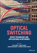
Early ROADMs that involved hundreds of discrete optical switches, dielectric filters, and occasionally variable optical attenuators were rats’ nests of fiber that rivalled the complexity of OEO switches. In fact, many early ROADMs comprised of solely a specialized subset of OEO switches. Today’s ROADMs, however, have benefited greatly from the evolution of technology and typically leverage either PLCs or wavelength‐selective switches (WSS) to more tightly integrate necessary functionality, thus helping to reduce ROADM complexity, and boost stability.
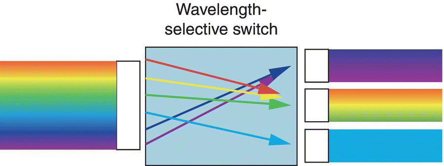
Figure 10.3 ROADM employing wavelength‐selective switching.
Today, several classes of ROADMs are in use especially by bandwidth network providers, thus enabling wavelengths to be switched as necessary with fluctuations in traffic requirements. Integrated optical attenuators has the ability to automatically rebalance channels as and when networks are reconfigured or new wavelengths are turned up, thus enabling add/drop wavelengths to be assigned to a fixed physical port on network equipment. This helps in minimizing bandwidth and enabling wavelengths to be switched not only between bypass and add/drop, but also in any network direction. State‐of‐the‐art directionless ROADMs convey myriad benefits such as the ability to build mesh networks, to supplement fiber protection with path protection, and to adopt agile optical networking.
10.2.4 A hybrid approach
In the face of relentless growth in bandwidth consumption that threatens to outpace the growth of their own core Generalized Multi‐Protocol Label Switching (GMPLS) IP networks, several bandwidth providers are turning to switching approaches which are optically hybrid as the solution to their predicament. Hybrid network architectures combine any and all optical switching technologies in an attempt to find the best balance of features for the intended application.
This section gives an overview of how multiple techniques may be combined to create a more efficient switched network. The core OEO IP routers are scaled as rapidly as possible and are used for packet‐level switching granularity. OEOs are surrounded by ODUs that serve two functions. First, all encapsulated IP traffic that is not needed at the network node can bypass the router. Second, legacy SONET/SDH traffic can be switched around the core routers or offloaded to ADMs if needed.
ROADMs are used for switching at the wavelength level of granularity, again serving multiple purposes. First, the IP core routers may be interconnected as a mesh, allowing packets to travel the most direct path rather than around a ring. Second, path protection is provided in addition to traditional ring protection techniques. Third, an entire wavelength may be optically amplified and/or regenerated and passed around the ODU and IP packet switches.
Although at first glance using multiple optical‐switching technologies might appear to be overly complex, it actually ends up greatly simplifying the overall network, as each type of information carried is properly routed around the network and only processed when absolutely needed. Coexistence of multiple optical switching technologies is likely to continue for some time now, given that bandwidth providers’ capabilities and cost requirements in optical switching are likely to vary across their networks.
10.3 Optical Transponders
10.3.1 WDM Transponders: An Introduction
Owing to the mammoth development of wavelength division multiplexing (WDM) technology for networking, there is an increase in the volume of network traffic and thereby the demand for greater bandwidth is continuously increasing. For conversion of operating wavelength of the incoming bitstream to a wavelength that is compliant to the networking system, WDM transponders proves to be the most vital component in such systems. Being a vital technology in the optical fiber networks, WDM technology is setting itself as the baseline for the future all‐optical networking systems. Most of the researchers are presently working on ways and means to optimize the WDM network. The most important component of the WDM network, for this purpose, is the transponder, which is basically a device which is used to optimize the performance of the WDM network.
Today’s optical network mainly relies on the WDM technology. Wavelength Division Multiplexing underlines the principle of assigning an independent dedicated wavelength to a single service of the network which is then multiplexed to a single optical fiber, thus eliminating the requirement of employing several such fibers. Besides, there is also an increase in the capacity of the fibers, which proves the enormous benefits that WDM system provides to both the service providers as well as to the receiving end users. The integral part of these WDM systems is the optical transponders as they serve as the most crucial medium for signal transmission of the entire system.
10.3.2 Basic Working of Optical Transponders
An optical transponder, better termed an OEO (optical‐electrical‐optical) transponder, is a device unit which basically converts optical to electrical and back to optical wavelength. Optical transponders have been utilized in diverse networks and are a potential candidate for several applications.
An optical transponder consists of a transmitter section and a receiver section, which is herein referred to as a responder, but they are functionally similar. It has the ability to cover wide ranges of transmission owing to wavelength conversion and signal amplification or regeneration. A transponder performs the function of receiving a signal, then amplifying it and finally re‐transmitting the signal with a different wavelength, thereby retaining the original data or signal content. The signal that is received by a transponder is optical in nature, which is transduced to its electrical counterpart, and finally the processing of these electrical data takes place. Before transmitting, the transponder is responsible for converting this electrical signal to optical signals mainly in the form of CWDM (coarse WDM) or DWDM (dense WDM) wavelengths. Thus the process of OEO (optical to electrical to optical) conversion is well established by the transducer. In contrast to ordinary electrical transmission, the regeneration in present day WDM transponders is facilitated by the concept of reshaping, retiming and reamplifying the signal to a close proximity of accuracy.
Figure 10.4 depicts the working of a bidirectional transponder where the transponder is placed exactly midway between a transmitting device and an optical DWDM system [18]. It may be well observed that the transponder receives an optical input from the left, which operates at fixed wavelengths of 1310 nm or 1550 nm. The transponder then converts this input wavelength to an ITU‐compliant wavelength, as seen on the right, and finally results in transmitting it to the output DWDM system. This entire process gets reversed when looked back from the receiving end. In such case, the ITU‐compliant data serves as the input to the transponder, which is finally converted back to the optical signal that is obtained by the client on the receiving end.

Figure 10.4 Working of an OEO transponder.

Figure 10.5 Schematic block of optical transponder.
Source: [19].
An optical transponder basically works as a wavelength regenerator that is responsible for converting an optical signal to its corresponding electrical signal, thereafter generating an exact replica of the input optical signal so as to use this signal to finally generate signals at different optical wavelengths, thus resulting in optical‐electrical‐optical conversion. The significant characteristics of optical transponders are that it has the ability to receive, amplify and re‐transmit a particular signal to an altered wavelength without distorting the content of the input optical signal. The client may be electrical or optical (operating at frequencies 1310 nm or 1550 nm), which may be either co‐located or are positioned at a certain distance. The interface may be lined by fibers, Coarse Wavelength Division Multiplexers (CWDM), or Dense Wavelength Division Multiplexers (DWDM). Figure 10.5 depicts a basic block diagram of an optical transponder [19].
10.3.3 Necessity of Optical Transponder (OEO) in WDM System
In recent times, the optical transponder has become very much a necessity in WDM system network for several reasons, as listed below.
Firstly, if a network comprises of different equipment operating at varying wavelengths urge to communicate amongst themselves within the network, a problem of incompatibility may arise. The optical transponder has the capability to address and overwrite such issues.
Additionally, there may be situations where several service providers provide optical fibers that are designed to meet different standards. Under such scenario, a WDM transponder enables traversing from one optical network to another within the system.
10.3.4 Applications of Optical Transponders
Optical transponders are widely used in WDM networking in addition to several other applications. The most commonly employed applications of optical transponders are stated below.
- Multimode to single‐mode conversion: Optical transponders have the ability to convert multimode fibers to single‐mode ones, with designs for short‐distance to long‐distance lasers, and/or 850 or 1310 nm to 1550 nm wavelengths conversions documented so far. The optical transponder module obeys all networking protocols and independently operates irrespective of the adjoining wavelength channels.
- Dual fiber to single fiber conversion: Inter‐conversions between dual fiber and single fiber is very much required for design of any networks. In case of dual fibers, a single wavelength is transmitted over two distinct fiber strands, while in case of single fibers both the wavelengths are transmitted over a single fiber strand, thereby enabling a bidirectional transmission mechanism. Two optical transponders are required for the purpose of dual fiber switching, while a single fiber has the capability to transmit two different wavelengths over a single fiber channel, as they can transmit and receive from either end.
- Introduction of additional fiber path: An optical transponder module may also independently include an additional (often treated as redundant) fiber path option for supplementary protection. The additional fiber path allows transmission of the input optical signal to two separate optical channels which are directed towards the two redundant receivers at the receiving terminal. Under any condition, the loss of the primary path would result in switching on the backup receiver. The said phenomena is electronically controlled, which results in much faster and more reliable operation.
- Optical repeaters: For the purpose of long‐haul communication, WDM transponders have been reported to function as repeaters in order to expand the distance of network by the process of wavelength conversion and optical power amplification. For employment as optical repeaters, the optical transponders regenerate the incoming signal effectively so as to traverse the optimum distance of desired transmission. With this option of signal regeneration, the degraded signal, as an outcome of the transmission process, may be debittered and retransmitted to achieve high quality of signal.
- Mode conversions: Optical transponders may be employed for the purpose of mode conversion. Converting modes result in quicker and simpler means of transmitting multimode optical signals to larger network distances employing a single‐mode fiber. It may be observed that most of the present day receivers are designed to have the capability of receiving both multimode and single‐mode optical signals over the same fiber.
- Wavelength conversions: It has been documented in literature that conversion of wavelengths employed in commercial networks even today is only carried out with the aid of optical transponders. It is known that the existing fiber‐based optical networks and interfaces naturally operate at the conventional wavelengths of 850 nm, 1310 nm and 1550 nm, thus implying that conversion to its corresponding CWDM or DWDM wavelengths is required to operate within the system.
10.3.5 Network Structure with Optical Transponder
The overall network system immensely benefits with the aid of optical transponders. In this section, two possible WDM ring network configurations which utilizes optical transponder are documented [20, 21].
10.3.5.1 WDM Ring Employing Line Network
A line network is a network formed by two point‐to‐point links between the nodes A‐B and B‐C respectively as shown in Figure 10.6. Each of these links are supported with optical transponders at the end points. The system works in such a fashion that if there is a failure in node B, nodes A and C would continue to communicate between each other as there is a bypass path established between the optical transponders which is adjacent to node B, thereby switching the transponders to the protection mode. Figure 10.6 shows the block diagram of a WDM ring line network.
10.3.5.2 WDM Ring Employing Star Network
A star network is so named because of the star‐like connection between the nodes, where all the other nodes A, C and D are connected to a star node B. The star node is backed up with a similar node which basically serves as a redundant node, as may be seen in Figure 10.7. In this type of configuration, the protection mode is switched from the star node to the redundant node once the star node fails to work.

Figure 10.6 Block diagram of line network over WDM ring.
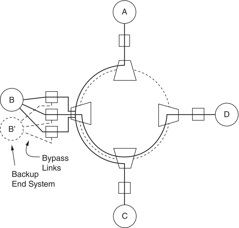
Figure 10.7 Block diagram of star network over WDM ring.
10.3.6 Differences Between Transponder, Muxponder, and Transceiver
In optical fiber networks, the transceiver and the muxponder perform similar functionalities to that of an optical transponder. They are mainly responsible for transmitting and receiving optical signals within the network [22]. Though being functionally similar, there are crucial difference between these three devices when considered from their design perspective and applications.
The transceivers employed to be used in optical fibers have limited functionality in terms of electrical‐optical serial transmission only. Optical transponders, on the other hand, may be used in parallel interfaces as well and performs wavelength conversion of optical signals without causing any signal distortion. WDM transponders can be thought of as two back‐to‐back placed transceivers. The fiber‐optic muxponders behave functionally similar to WDM transponders with the additional feature of multiplexing. The muxponder has the ability to multiplex several sub‐rate interfaces into an interface of much higher rate.
10.3.7 Summary
In WDM networking systems, optical transponders hold an extremely high position of interest which can never be underestimated. They form the underlying functionalities such as reception of optical signals, followed by amplification or regeneration of such signals and finally retransmission of this signal onto a completely different wavelength, thereby making it the most promising device in networking systems.
The optical transponders have also shown its versatility in several applications such as interconversion of signals including transmission shift from multimode fibers to single‐mode ones.
10.4 Performance Analysis Study of All‐Optical Switches, Electrical Switches, and Hybrid Switches in Networks
A comparative study of all‐optical switches, electrical switches, and hybrid switches in relation to data center networks as well as telecommunication networks is presented in this section. The simulation studies of the response time and the optimum output achieved so far documented reveal the advantages which the hybrid switches have over their electrical and all‐optical counterparts [23].
10.4.1 Introduction
The exponentially growing traffic mainly contributes to the demands of the present architecture of the Internet and to support our demands of the service in terms of its quality, class, and its type on an unified podium. The internet service utilized by us today is cored by over‐provisioned connection of utilities (technically called nodes), employing the most powerful present‐day technology of Wavelength Division Multiplexing (WDM). With the exponential surge of data traffic, there is a continuous and dynamic change of the patterns of data traffic with an enormous growth in data capacity that finally presses the requirement for a more versatile, agile, and scalable networking system which may have the ability to handle this data traffic efficiently.
Additionally, the increasing demand for data and managing data traffic has led to the birth of huge‐dimensioned data centers so as to ease the extraction of data easily. The present‐day data centers have expanded manyfold, thus leading to consumption of enormous power in the order of tens of megawatts. With the restrictions in power consumption, the data centers aim to result in higher productivities with a paradigm shift to optical switching technology which may be provisioned to be exploited. Today’s datacenters mainly rely on the trending components of electronic switches employing Ethernet or Infiniband [24, 25], which results in lower output and delayed system response.
In recent times, it has been reported that both in the telecoms sector as well in data centers, hybrid switch technologies besides all‐optical switching have been employed to take care of the huge data traffic effectively. This section aims to collate all similarities and differences of both the stated switching technologies in the light of state‐of‐the‐art electronic switches.
10.4.2 Optical vs. Electrical vs. Hybrid Telecom Switches
Literature reports that the present‐day telecom network both at the local and at the global level is formed by the interlocking of nodes, which have connection of the order of two to five distinct associated connections. Though the degree of the links may be thought of to be extremely small, the connection amongst the nodes has immensely high capacity, which ranges from hundreds of gigabytes per second to the order of terabytes per second. Dense WDM technology was the only hope for realizing such high‐capacity links within the network, where several varying wavelengths may be transmitted parallelly through the optical fiber link.
The connecting path from the transmitting to the receiving end is often connected through several nodes with multiple hops being present across it. The greater the number of hops within the network, the higher the latency is, thus increasing the overall response time. Typical telecom switches within the network are generally surrounded by the edge routers, which are mainly responsible for realizing functions such as aggregation of data packets and data traffic orientation such that the link is utilized within the network in the most efficient way possible. So if the switching system is designed with the aid of solely all‐optical switches, they turn out to be equally beneficial for electronic data processing as well.
An electrical switch, on the other hand, employs principles of Optical‐to‐Electrical and Electrical‐to‐Optical conversions at the input and output terminals respectively. The optical signals fed at the input of the switch are first transformed to their electrical counterpart and finally stored. The responsibility for scheduling the process and transmitting the input signals from the input buffer to the output buffer is done by the control plane. This results in extremely high switching capacity once all the incoming packets are made to cross the network traffic.
In order to realize such increased capacity electrical switches, smaller electrical switches are assembled either in serial to parallel configuration mode or in parallel to serial configuration mode to achieve high capacity. Each of the incoming data packets have to traverse several stages of processing, which in turn results in higher power consumption and high response time. In spite of this, the packet loss may be reduced to a greater extent if the buffer capacities can be significantly improved.
On the contrary, in case of all‐optical switches [26] as depicted in Figure 10.8, the data is potentially optical in nature while the control plane is devised to remain in the electrical domain. In order to increase the capacity for optical switches, exploiting the property of parallelism of wavelengths within the system is harnessed. To achieve higher speed and to ensure non‐blocking switching, an Arrayed Waveguide Grating Router (AWGR) may be employed for different wavelengths which would occupy parallel paths.
At the input of the switching network, tunable wavelength converters (TWCs) are positioned so as to enable proper routing of wavelengths from an input terminal to an output terminal. In order to maintain a synchronization in wavelengths between the input link and the output link, fixed wavelength converters (FWCs) are generally placed at the output end of such networks.
Although no mature optical buffer design has been so far documented in the literature, yet these switches have the ability to effectively use all the wave dimensions such as wavelength, space, and time domains [26]. Additionally, in the case of all‐optical switches, there is no concept of store‐and‐transmit processing or bit‐by‐bit processing, thus resulting in conservation of power as compared to its electrical counterpart. In order to route wavelengths within the network, the AWGR switching technology serves to be more passive and promising as it consumes no power.
In spite of the several similarities that the hybrid optical switch holds with respect to the all‐optical switch, there are certain differences. The lookback FLDs in the case of all‐optical switches are replaced by a loopback shared buffer system in the case of hybrid switches, which is depicted in Figure 10.9.
Figure 10.8 All‐optical switch design for telecom network.
Source: Based on [26].
An all‐optical switch has the capability to handle (w*m) inputs and outputs, where w represents the total number of incoming wavelengths to the switch. In contrast to this system, hybrid switches employ loopback shared buffer system which is generally designed to use only one input and one output line within the network.
Analogous to the all‐optical switch, the control plane of the hybrid optical switch upon contention first looks for dissimilar wavelengths which may be made available at the same output link. Once the situation develops such that all the wavelengths get occupied at the output link, the packets in such scenario would be sent back via the loopback shared buffer and would then wait for its turn for retransmission. A negative situation may arise if the shared buffer doesn’t have enough space to accommodate the package. Under such scenario, the packet would be dropped.
It is worth mentioning that the loopback shared buffer outperforms loopback FDLs owing to the fact that it introduces arbitrary delay due to the occupancy of fewer ports within the switching network. Once the transmission line is available, the delayed packet are then released. The setback of loopback shared buffer is that it consumes power due to its larger dimension, although researchers are working to reduce the size of this loopback shared system by exploiting multiplexing techniques statistically.

Figure 10.9 Optical hybrid switch design for telecom network.
In contrast to all‐optical switches, the optical hybrid switches are documented to produce lower response delay as transmission is initiated as soon as the transmission channel becomes available. In addition to this, the optical hybrid switches offer advantages by lowering the rate of packet dropping since it has the ability to hold the packet before the retransmission is set up.
10.4.3 Optical vs. Electrical vs. Hybrid Data Center Switches
Keeping in pace with the demands of modern technology, data centers have emerged to promote connection among hundreds or thousands of nodes within the network in contrast to the existing traditional telecom network switches. Additionally, data centers have been designed in such a fashion so as to reduce the latency originating between the end nodes. Data centers mainly focus on employing parallel transmission to meet the ever‐increasing user demands. In such a situation, latency delay in the order of nanoseconds might cause a drastic degradation in the overall system performance.
Electrical switches face restrictions on the number of ports it can handle. So the existing electrical switching system is based on employing several smaller electrical switches associated with smaller port counts which are assembled in such a fashion so as form larger system by assembling many such smaller counterparts [27], with the final aim of accumulating and interconnecting larger number of nodes. The major drawback of this kind of union structure lies in the fact that though the latency of smaller switch is less, when interconnected the number of hops increases, thus leading to a significant increase in the overall latency of the system.
The performance study documented in the literature makes use of a network called an electrical flatten butterfly network [28], which serves as an alternative to existing electrical switches. In order to compare, an optical switching fabric network like AWGR is used, which has the ability to provide higher values of ports compared to an electrical switching fabric network, thereby resulting in greater number of interconnections to the end nodes compared to those in an electric switch.
A requirement for a multi‐stage switching system may arise, especially when connection of hundreds or even thousands of nodes is desired, and simultaneously the number of switches required would also reduce, thereby making the network design even much simpler.
An optical hybrid switching architecture [29], which has been mainly designed for data centre networks, is depicted in Figure 10.10. In comparison to the optical hybrid switches which are employed for telecom networks, the similar switching technology which is designed to be used for the data centers does not require FWCs at the output terminal of the switching network. Additionally, the switches used in data centers are designed to meet asymmetric link capacity between the incoming and outgoing links in order to achieve the benefits that wavelength parallelism promotes.
Figure 10.11 depicts an all‐optical switch design that is typically used in data centre networks. The switch is designed to replace the shared loopback buffer used in telecom networks with multiple fiber links (FDLs).
The electrical flatten butterfly network has been observed to have an extremely poor performance when compared to the other two other combinations of optical switches. The response time in this switching mechanism is comparatively slow, thereby decreasing the effective bandwidth even at lower incoming packet range. On the other hand, both all‐optical switches and optical hybrid switches are seen to have very poor latency for most network configurations. The hybrid optical switch is expected to provide its best performance in terms of latency and hence serves to be the best possible candidate for data center switches.

Figure 10.10 Optical hybrid switch (DOS) design for data center network.
Source: [29].

Figure 10.11 All‐optical switch design for data center network.
10.4.4 Summary
This section consists of a detailed comparison of all‐optical switches, electrical switches, and optical hybrid switches which were designed to work in both telecommunication networks and data center networks. Owing to the significant measurements, such as latency, throughput, and power consumption, optical switches has been observed to have outperformed other electrical switches. The lowest latency is achieved by the optical hybrid switch, but this suffers drawbacks in terms of greater power consumption compared to the all‐optical switch.
10.5 Electrical and Optoelectronic Technology for Promoting Connectivity in Future Systems
Optical interconnects have been reported to surpass the most important figure of merit, i.e., the bandwidth‐distance product beyond the historic figure of 100 Gbps/meter, while the advances in CMOS technology and signal processing have made it possible for electrical interconnects to break the barrier of 500 Gbps/meter as documented so far, to approach the level of optical interconnects [30].
10.5.1 CMOS Technology
In the last few decades, there has not been much significant improvement in the performance of transistors, and researchers have been able to achieve only a marginal improvement in terms of lowering the power consumption during operation. This has resulted in limits to incorporating larger number of transistors in a smaller space and hence not much refinement as regards density can be achieved. To overcome this, employing multicore parallel architectures has been considered as an alternative to meet the ever‐increasing demand [31–35].
In order to achieve the targeted performance, parallel architectures may be required, and interconnect technology is the key to enable it. There are certain drawbacks to these interconnects such as system throughput, increased latency and system density, which pose a major bottleneck to system performance, thus hindering further advances for future architectures.
The solution of choice to define the future of networking has always been a debatable topic ever since the emergence of optical and electrical interconnect technologies as to which should be the best possible candidate in this regard. Both the stated technologies offer trade‐offs depending on applications, which may based on power consumption, reliability, density of integration, and even cost.
Network system engineers had been initially reluctant to replace electrical interconnects, which were basically cumbersome, in favour of better optical solutions, which offered advantages such as lower complexity and lower cost (typically when used for longer distances), until in places the electrical interconnect was deemed to be the only possible solution. In the recent times, optics have been seen to outperform its electrical counterpart as most of the present generation of technologies entirely rely on it due to its extremely high‐performance matrix. Again, it too suffers drawbacks owing to the cost advantage that the electrical interconnects possess. So optical interconnects have suited themselves for applications in longer distances, where attenuation seems to be a major hindrance for electrical interconnects.
Future technologies might face some other factors for design depending on the future requirements and may smash the existing paradigms. Optimizing the trade‐offs for the existing solutions, and examining the requirements and applications for future‐generation systems, would be a potential domain of research.
10.5.2 Considerations for Selection of Interconnects
There are several factors which are responsible for the selection of the best alternative to meet the requirements of any system. The selection of interconnect technology is mainly taken into consideration depending on the targeted application.
An important figure to take into consideration for any interconnect selection is the throughput of the device, which may be defined as the throughput of the transmitter when added to the throughput of the receiver that has the possibility of being integrated on a single chip. The power consumed by the transceiver and its total design area pose limitations to obtaining the maximum throughput for any device. Larger dimensions of transceivers possess fabrication and manufacturing issues.
Throughput‐distance product (Gbps/meter) is a metric that is being mostly used to evaluate the performance of an interconnect, by in turn evaluating the throughput‐distance or bandwidth‐distance products [36]. The value of this metric remains constant for a given interconnect technology.
Optical interconnects have always proved to be a better candidate as they offer superior bandwidth compared to other existing technologies. Research reveals the fact that optical links have advantages over electrical links at the throughput of 100 Gbps/meter [37–39]. They have a bottleneck due to the additional area they require to embed the optical functionalities which limits their effective density.
Another important figure to consider is the cost involved with interconnect manufacturing. Economical interconnects would always be at the forefront. The total cost involved depends on several factors such as the cost of the individual components, manufacturing cost, and deployment cost. There is always an additional cost associated with optical interconnects as these rely on components such as lasers, lenses, optical substrates, optical sources, and photodetectors as well as the components, resulting in their interconnections which are non‐existent in case of electrical interconnects. Although the optical technology has the capability to integrate most of the components within the chip, the optical source, being the key element, fails to be integrated owing to its cooling purpose [40–42].
The advantages of electrical interconnects lie in the fact that higher level of interconnections is achievable owing to CMOS technology without the requirement of any associated components as was in the case of optical solutions. Signal conditioning may be required, depending upon which electrical links introduce insertion loss compensation [43], and which requires Reed–Solomon (RS) forward error correction (FEC) [44].
The most important concern is the interconnect reliability, which becomes a prime concern in larger systems employing several nodes, as a single nodal failure may result in the entire network failure if they are not addressed correctly on time. The susceptibility of failure of optical interconnects are higher as they involve the use of several additional components.
With the advancement in integrated circuit technology, there is a paradigm shift to faster and more power‐efficient FinFet devices, and researchers claim that electrical interconnects will still remain in data centers as well as in the communications chassis well beyond 2020 [45].
10.6 Conclusion
Over the past decade, there has been an enormous hue and cry for higher data rates, which led to the design of switching technologies so as to guide the network with minimum or no system‐generated loss. Standing at this juncture, which optical switching technology is the best continues to be a fiercely debated topic. OEOs, ODUs, and ROADMs have each taken a turn as the proposed optical switching technology to end all optical switching technologies.
ROADMs (especially multi‐degree varieties) were for a time regarded as the end game in optical switching. Then PICs and PLCs came along, and there was a surge of predictions that higher‐density integration would favor the use of Optical‐Electrical‐Optical (OEO) switching. Recently, ODU switching has again made a comeback in the field of switching technologies.
In reality, each of these switching categories has its pros and cons, and identifying the optimal approach and determining a trade‐off as to whether one of the increasingly prevalent hybrid options is appropriate depends upon a particular bandwidth provider’s infrastructure and the applications which it is designed to address.
Bibliography
- 1 J.R. Hamilton. An architecture for modular data centers. CIDR, 2007. arXiv:cs/0612110.
- 2 H. Wu, G. Lu, D. Li, C. Guo, and Y. Zhang. A high performance network structure for modular data center interconnection. ACM CoNEXT’09, 2009.
- 3 B. Canney. IBM portable modular data center overview. http://www‐05.ibm.com/se/news/events/datacenter/pdf/PMDC, Introducion‐Brian Canney.pdf, 2009.
- 4 HP Performance Optimized Data center, ftp://ftp.hp.com/pub/c‐products/servers/pod/north_america _pod_datasheet 041509.pdf.
- 5 S. McNealy, V. Khosla, A. Bechtolsheim, and B. Joy. Sun Modular Data center. http://www.sun.com/service/sunmd, 2010.
- 6 N. Farrington, G. Porter, S. Radhakrishnan, H.H. Bazzaz, V. Subramanya, Y. Fainman, G. Papen, and A. Vahdat. Helios: A hybrid electrical/optical switch architecture for modular data centers. SIGCOMM’10, 2010.
- 7 K.V. Vishwanath, A. Greenberg, and D.A. Reed. Modular data centers: How to design them? Proc. of the 1st ACM Workshop on Large‐Scale System and Application Performance (LSAP), 2009.
- 8 C. Guo, G. Lu, D. Li, H. Wu, X. Zhang, Y. Shi, C. Tian, Y. Zhang, and S. Lu. A high performance, server‐centric network architecture for modular data centers. ACM SIGCOMM, 2009.
- 9 K.J. Barker, A. Benner, R. Hoare, A. Hoisie, A.K. Jones, D.K. Kerbyson, D. Li, R. Melhem, R. Rajamony, E. Schenfeld, S. Shao, C. Stunkel, and P. Walker. On the feasibility of optical circuit switching for high performance computing systems. SC’05, 2005.
- 10 M.F. Tung. An Introduction to MEMS Optical Switches. https://courses.cit.cornell.edu/engrwords/final_reports/Tung_MF_issue_1.pdf, 2001.
- 11 D. Vantrease, R. Schreiber, M. Monchiero, M. McLaren, N.P. Jouppi, M. Fiorentino, A. Davis, N. Binkert, R.G. Beausoleil, and J.H. Ahn. Corona: system implications of emerging nanophotonic technology. ISCA’08, 2008.
- 12 G. Wang, D.G. Andersen, M. Kaminsky, M. Kozuch. T.S. Eugene Ng, K. Papagiannaki, M. Glick, and L. Mummert. Your data center is a router: The case for reconfigurable optical circuit switched paths. ACM HotNets’09, 2009.
- 13 A.G. Eantc. Arista 7148SX Switch. http://www.aristanetworks.com/en/7100_Series_SFPSwitches, 2009.
- 14 Calient Networks. http://www.calient.net, 1999.
- 15 Cisco Data Center Infrastructure 2.5 Design Guide. www.cisco.com/application/pdf/en/us/guest/netsol/ns107/c649/ccmigration_09186a008073377d.pdf, 2013.
- 16 P.M. Zeitzoff. 2007 International Technology Roadmap: MOSFET scaling challenges, Solid State Technology, 51(2):35, 2008.
- 17 J. Theodoras. Contemporary categories of optical switching. https://www.lightwaveonline.com/network‐design/dwdm‐roadm/article/16649750/contemporary‐categories‐of‐optical‐switching.
- 18 Tutorials of fiber optic products. https://www.fiber‐optic‐tutorial.com/category/network‐solutions/wdm‐optical‐network/optical‐transponder, 2017.
- 19 Fiber optic solutions. https://www.fiber‐optic‐solutions.com/optical‐transponder‐o‐e‐o‐wdm‐network.htm, 2017.
- 20 A.V. Krishnamoorthy. The intimate integration of photonics and electronics. Advances in Information Optics and Photonics. SPIE, 2008.
- 21 R. Ramaswami and K. Sivarajan. Optical Networks: a Practical Perspective. San Francisco, Morgan Kaufmann, 2002.
- 22 Irving. The versatile optical transponder (OEO) in WDM system. https://community.fs.com/blog/the‐versatile‐fiber‐optic‐transponder‐oeo‐in‐wdm‐system.html, 2015.
- 23 X. Ye, V. Akella, and S.J.B. Yoo. Comparative studies of all‐optical vs. electrical vs. hybrid switches in datacom and in telecom networks. Optical Fiber Communication Conference/National Fiber Optic Engineers Conference, 2011.
- 24 InfiniBand Architecture Specification, Volume 1, Release 1.0. http://www.infinibandta.org/specs, 2002.
- 25 Voltaire Vantage 8500 Switch. http://www.voltaire.com/Products/Ethernet/voltaire_vantage_8500, 2009.
- 26 H. Yang and S.J.B. Yoo. All‐optical variable buffering strategies and switch fabric architectures for future all‐optical data routers. Special Issue on Optical Networks, IEEE/OSA Journal of Lightwave Technology, 23(10): 3321–3330, 2005.
- 27 Al‐M. Fares, A. Loukissas, and A. Vahdat. A scalable, commodity data center network architecture. SIGCOMM '08, 2008.
- 28 J. Kim, W.J. Dally, and D. Abts. Flattened butterfly: a cost‐efficient topology for high‐radix networks. 34th Annual International Symposium on Computer Architecture (ISCA), 126–137, 2007.
- 29 X. Ye, P. Mejia, Y. Yin, R. Proietti, S.J.B. Yoo, and V. Akella. DOS – A scalable optical switch for data centers. ACM/IEEE Symposium on Architectures for Networking and Communications Systems (ANCS), 2010.
- 30 R. Farjadrad. What’s the difference between optical and electrical technology for 100‐Gbit/s connectivity in future systems?. https://www.electronicdesign.com/technologies/communications/article/21800130/whats‐the‐difference‐between‐optical‐and‐electrical‐technology‐for‐100gbits‐connectivity‐in‐future‐systems, 2014.
- 31 G. Kalogerakis, T. Moran, T. Nguyen, and G. Denoyer. A quad 25Gbps 270mW TIA in 0.13um BiCMOS with, 0.15dB crosstalk penalty. ISSCC Dig of Tech Papers, 116–117, 2012.
- 32 T. Tekemoto, et al. A 4x25Gb/s 4.9mW/Gbps‐9.7dBm high sensitivity optical receiver based on 65 nm CMOS for board‐to‐board interconnects. ISSCC Dig of Tech Papers, 118–119, 2012.
- 33 J.Y. Jiang, et al. 100Gb/s Ethernet chipset in 65nm CMOS technology. ISSCC Dig of Tech Papers, 120–121, 2012.
- 34 S. Parikh, et al. A 32Gb/s wireline receiver with a low‐frequency equalizer, CTLE and 2‐tap DFE in 28nm CMOS. ISSCC Dig of Tech Papers, 28–29, 2012.
- 35 Y. Doi, et al. 32Gb/s data interpolator receiver with 2‐tap DFE in 28nm CMOS. ISSCC Dig of Tech Papers, 36–37, 2012.
- 36 A.V. Krishnamoorthy, K.W. Goossen, W. Jan, et al. Progress in low‐power switched optical interconnects. IEEE Journal of Selected Topics in Quantum Electronics, 2011.
- 37 M.A. Taubenblatt. Optical interconnects for high‐performance computing. IEEE Journal of Lightwave Technology, 2012.
- 38 B.E. Lemoff, et al. Demonstration of a compact low‐power 250Gbps parallel‐DWM optical interconnect. IEEE Photonics Technology Letters, 220–222, 2005.
- 39 F.E. Doany, et al. Terabit/s‐class 24‐channel bidirectional optical transceiver module based on TSV Si carrier for board‐level interconnects. Proc 23rd Annual Meeting IEEE Photon Society, 564–565, 2010.
- 40 D. Gockenburger, et al. Advantages of silicon photonics for future transceiver applications. Proceedings of 36th Euro Conference on Optical Communication, 1–6, 2010.
- 41 D.V. Thourhout. Si Photonics. Proceeding of Optical Fiber Communication Conference, 2012.
- 42 H. Thacker, et al. Hybrid integration of silicon nano‐photonics with 40 nm‐CMOS VLSI drivers and receivers. Proc. IEEE 61st Electronic Components Technology Conference, 829–835, 2011.
- 43 S. Ibrahim and B. Razavi. A 20Gbps 40mW equalizer in 90nm CMOS technology. ISSCC Dig of Tech Papers, 170–171, 2010.
- 44 P. Dave and J. Petrilla. Proposal for FEC in40G/100G ethernet. IEEE 802.3 Ethernet Working Group Proposals, 2008.
- 45 E. Wu. A framework for scaling future backplanes. IEEE Communication Magazine, 188–194, 2012.