8
Liquid Crystal Switches
Swarnil Roy1,2 and Manash Chanda2
1 IEEE SSCS Kolkata chapter, Kolkata, West Bengal, India
2 Department of Electronics and Communication Engineering, Meghnad Saha Institute of Technology, Kolkata, West Bengal, India
8.1 Introduction
Bandwidth demand in modern communication systems calls for optical communication links and networks. Optical switches are an integral part of optical communication networks and optical sensing architecture because they can dynamically control the optical path connection. But if there is any optical to electrical conversion in the path that would crunch the bandwidth, all‐optical switches are preferred in that context. Also, optical switches with no moving parts ensure high stability and reliability.
But it is also important to identify specifically where to apply liquid crystal (LC) technologies, as they have limitations as regards response time, which is not less than several microseconds. The main focus of this chapter is the purpose of LC optical switches in space switching (telecom and sensor applications), in protection and recovery applications, and optical add/drop multiplexing, which need fewer restrictions about switching time.
Networks that can detect a failure and have an additional path in order to maintain the transmission when failure is detected are called protection and recovery networks. Optical add/drop multiplexer (OADM) is an optical multiplexer which insert or extract optical wavelengths to or from the wavelength division multiplexing (WDM) optical transmission stream. Literatures have also referred to some reconfigured version of OADM (ROADM) [1]. These can be building blocks for an optical cross‐connect (OXC); OXC is a switching matrix for incoming optical wavelength, where it provides a path from one input optical channel to any output channel. As an example, it is reported that the switching time of an OXC is within a few tens of milliseconds [2]. It should be mentioned also that the determination of the minimum response time required for WDM, transport network restoration, or flexible bandwidth allocation depends on several network management and service‐related issues. On the other hand, LC‐based switches are not suitable for packet switching applications which require a faster switching time (in the nanosecond range) [3]; hence, they will not be considered here.

Figure 8.1 General optical switch block diagram.
Before getting into LC optical switching trend, it is important to have a brief understanding of the optical parameters [4]. For that purpose, we are considering only one active input with incoming power (Figure 8.1).
Insertion loss (IL): This is the ratio between the input signal power to output signal power, which is a measure of lost signal power between an input and an output‐connected port of the switch. This loss is measured in decibels as given in the expression below and must be as small as possible.
Crosstalk: This is the fraction of the power leaked to the non‐switched output port from the input port. It is a measure of the signal interference between channels. This ratio should be low. Here ![]() is the power of the non‐switched port.
is the power of the non‐switched port.

Switching time: Switching time is generally expressed in terms of IL. It is the time required for IL of the switch path to achieve 90% of its final value from the moment the switching command is placed.
Polarization‐dependent loss (PDL): This is measured as peak‐to‐peak difference between orthogonal states of polarization for transmitting light. Optical switches must have low PDL (typically <0.5 dB).
Power consumption: The electrical power required for the switching operation.
Bit Rate: The number of bits per second that the optical switch can manage to transmit.
Polarization Mode Dispersion (PMD): It occurs due to the fact that in a channel various states of polarization travel at slightly different speeds. When they pass through the switch these polarized lights create a lag between each other and that leads to PMD.
LC switches, in general, have the following advantages: they offer very low IL – less than 6 dB to access 40–80 channels. They also provide good CT (better than −40 dB) [5], low PDL and power consumption, and higher transmission capability (bi rate). They have no moving parts for switch reconfiguration and the technology has matured over time. What makes LC switches so attractive is that it provides all these at the same time, whereas other technologies could have one or two of these advantages but not all. Also, bearing in mind the recommendations of the Kyoto Protocol and Intergovernmental Panel on Climate Change, low power consumption has become essential and there is a need to reevaluate and reduce Information and Communication Technologies’ Impact on the Energy Footprint; and LC in switching matrices might do just that.
In the next topics, we are going to review LC materials properties and principles, then a description of the main types of switches based on the mechanisms used for steering light, their parameters, and specific applications are presented.
8.2 Liquid Crystal and Its Properties
Liquid crystal (LC) has proved to be an important functional organic material in various hi‐tech products surrounding us. The history of LCs can be traced back to the discovery of an optical property in cholesterol. Despite the appearance of a cloudy fluid, cholesterol displays an optical anisotropy (birefringence) like a crystal below a critical temperature Tc.
LCs essentially are substances whose molecular order, depending on the ambient temperature, is intermediate between that of crystalline solids and that of amorphous liquids. Some of their properties (like dielectric constant and refractive index etc.) are like crystalline solids. That is why the optical properties of LC can be modified using applied electric field.
Liquid crystal materials generally have several common characteristics. Among these are a rod‐like molecular structure, rigidness of the long axis, and strong dipoles and/or easily polarizable substituents. These sharp anisotropic rod‐like molecular structure (in some cases they are disc like) found in LC are called mesophases [6]. The orientation of these rod‐like structures depends on temperature. As temperature is decreased to be low, the molecules show an orientational order with the molecular axis oriented in a particular direction, but they do not have a positional order (nematic phase, N). Decreasing the temperature further, the molecules show more and more ordered and layered structure, ultimately tending towards complete crystalline solid (Sematic‐A, Sematic‐C, Crystalline solid). On the other hand, this regular layered orientation can be achieved by applying electrical potential.
8.3 LC Structures for Optical Switching
As mentioned above, LC, having no movable part, is a promising candidate for optical switching in telecommunication. In this section we would discuss different LC structure for optical switching. Most popular structures are twisted nematic (TN) devices and surface‐stabilized ferroelectric liquid crystals (SSFLC) [7–10]. Another structure based on polymer‐dispersed liquid crystal (PDLC) has also been reported in recent literature [11–13].
8.3.1 Twisted Nematic (TN) cells
Though TN liquid crystals are the mostly used in the display systems, it can be used for optical switching as well. In these cells both planar and perpendicular alignment can be used. Because of its twisted nature, the LC molecules perform a 90° twist through the thickness of the LC cell. Thus, a linearly polarized light goes through a 90° phase shift provided it satisfies Mauguin condition: ![]() , where d is the cell thickness, ∆n is the LC birefringence and λ is the light wavelength.
, where d is the cell thickness, ∆n is the LC birefringence and λ is the light wavelength.
In display devices with TN cells, there are two linear polarizers in between LC layer. Depending on their orientation, TN cells can be made in either a normally black mode or normally white mode. In most display applications, two crossed polarizers are placed with the transmissive axis of each polarizer parallel to the rubbing direction of each alignment layer, operation of a TN device in this mode is normally white (NW) mode. In OFF state (no applied voltage) the incident light is transmitted, but when a voltage is applied molecules reorient themselves and block the light. A LC cell from an electrical point of view, acts as a capacitor with a non‐ideal dielectric material whose electrical equivalent can be obtained using an experimental procedure based on the impedance spectroscopy technique reported in [14–16]. The equivalent circuit consists of voltage‐dependent capacitor (CLC) with series (RS) and parallel (RP) resistors as shown in Figure 8.2. The magnitude of CLC for 1 cm2 TN cell with of 5 μm thick LC is also depicted in Figure 8.2. The threshold (usually 1–2 V) and switching (usually 3–5 V) voltages can be derived from this electrical modelling.
CLC varies with applied voltage due to the dielectric permittivity modifications as a result of molecular reorientations. At low voltages (below Vth) the capacitance is constant, but a nonlinear variation can be obtained if the voltage is increased after that. Finally, the capacitance remains almost constant for voltages greater than Vsw. Power consumption and response time of the TN device estimated from equivalent circuit simulation are of the order of nW and a few tens of ms respectively. The transmission factor for monochromatic polarized light can be calculated using Jones matrices [17] given as:

where ![]() and T0 = maximum transmission.
and T0 = maximum transmission.
Typically, ![]() is used in practical devices, since a smaller u gives a smaller cell gap and a faster response speed [18]. It should be mentioned that once contrast is maximized for a wavelength, optical transmission would vary for other λ. But this dependence can be reduced.
is used in practical devices, since a smaller u gives a smaller cell gap and a faster response speed [18]. It should be mentioned that once contrast is maximized for a wavelength, optical transmission would vary for other λ. But this dependence can be reduced.
A simple polarization‐independent liquid crystal Fresnel lens using the surface‐mode switching of 90 twisted nematic liquid crystals (TN‐LCs) is reported in recent literature [19]. This proposed structure reduces the transition time to a few milli‐seconds under the surface‐mode switching. Response time can be further improved by the use of low‐viscosity LC materials and the transient nematic effect [20]. A hybrid‐aligned nematic LC structure displays promising sub‐millisecond response time [21]. Response time of such structures is reported as 0.75 mS experimentally. Another sub‐millisecond response time has been reported for Bidirectional Field Switching Mode using inverse TN structure [22].

Figure 8.2 (a) Electrical equivalent of TN cell and (b) variation of capacitance with applied voltage.
8.3.2 Surface‐Stabilized Ferroelectric Liquid Crystal (SSFLC) Cells
In these devices, the ferroelectric LC material is sandwiched between two very thin (a few micrometers each) LC layers. A variety of molecular orientations exists for SSFLC [23], but the bistable bookshelf layer structure is most common one. In these materials, there is a tendency to create a unwanted helical formation due to macroscopic spontaneous polarization which must be stabilized [24]. The response time is a few microseconds but with a memory effect (bistability). In the presence of an electric field, the molecular orientation changes which is a rotation of the smectic cone driven by coupling between the polarization and the electric field, the device remains in this state until a reverse polarity voltage is applied. An electrical modeling of these devices that predicts switching voltage (a few volts), power consumption (nW), and response time (a few microseconds) in such devices as a function of fabrication parameters is reported in [25].
When an SSFLC device is placed between crossed polarizers, with one of them parallel to the molecular axis of one of the stables states, one of the two states will be black. Optical transmission can be calculated using the Jones calculus, and is given by:

Here To is the maximum transmission between parallel polarizers, θ is the cone angle of material (optimal value is 22.5°) and d is the thickness of the device which should be maintained at d = λ/2∆n for optimal working. Like TN cells, the device performance is optimal for a given λ, but compared to TN cells optical transmission for other wavelengths varies much abruptly.
8.3.3 Spatial Light Modulator (SLM) Cells
A SLM modulates an optical beam’s amplitude, phase, or polarization, using the birefringence properties of the LC cell in one or two dimensions. 2D LC SLMs are mostly electrical but optically addressed analog light valves are also proposed [26]. The spatial structure of an electrically addressed SLM is shown in Figure 8.3. The pixel pitch p is defined as spacing between two adjacent pixels and pixel gap i is the edge‐to‐edge spacing between adjacent pixels. Assuming square pixels, the geometrical fill factor F is defined as the ratio (p/i)2 and this parameter puts an upper bound to the SLM optical efficiency. Most LC SLMs are panels consisting of a LC layer aligned between two glass sheets, with a thin‐film transistor (TFT) control circuitry. Major drawbacks are rather large pixels and moderate ‘fill factor’ (<60%) due to large dead areas between TFTs. Lack of flatness is also a problem specially if the modulated beam is coherent.
More compact SLMs are obtained with the liquid crystal on silicon (LCOS) technology [27, 28]. The device structure consists of a LC layer sandwiched between a reflective silicon backplane and a transmissive counter‐electrode shown in Figure 8.4.

Figure 8.3 Two‐dimensional SLM geometry.

Figure 8.4 LC on silicon SLM geometry.
Source: [29]/MDPI/CC BY‐4.0.
Using VLSI integration process, light and flat displays with high‐definition (1920 × 1080), high‐ resolution (pixel pitch < 8 μm), and high fill factor (>95%) can be manufactured. Though main applications of LCoS SLMs are high‐definition display, beam‐steering for optical tweezers [30], optical switching matrices, or wavelength‐selective switches (WSS) [31] can be implemented using this as well. But the characteristic of LCoS must be taken into consideration while designing optical fiber system [32].
8.4 Liquid Crystal Switches
Liquid crystal switches can be distinguished based on the light steering mechanisms with LCs, such as reflection, wave‐guiding, polarization management, or beam‐steering (planar or volume). Some of them are summarized in this section and compared against their switching parameters and applications.
8.4.1 Optical Crystal Switching Architectures
Optical space switches can be implemented in two architectures, namely, broadcast‐and‐select (BS) and space routing (SR). In BS switching, the incoming light information from a channel is split to all output channel array through an intermediate blocking stage. Switching the blocking stages ON and OFF would then select the desired output channel. In Figure 8.5 we can see a possible architecture for BS switches. We can see that from source, light information is going to channels 2, 3, and 4 via the blocking stage and due to the status of the blocking stage only channel 2 receives the signal. If the blocking stage is implemented by amplitude modulators, high contrast ratio needs to be maintained to avoid crosstalk. This scheme suffers from large complexity of the intermediate stage when the number of channel increases (2D input array require 4D selection mask) and a very poor power budget which forces optical amplification in this case.

Figure 8.5 Broadcast‐and‐Select (BS) switch architecture.
The SR scheme is more suited for LC switching. In driving the information from an input to an output channel it exploits an orderly arranged SR intermediate element. If the number of switching elements is limited, this scheme can limit the IL as for the Benes or Banyan topologies [33].
Implementation of SR switches by individual light steering can be exercised in two ways: a multi‐stage planar topology using arrays of 2 × 2 binary polarization switches [34] or single‐ and dual‐stage schemes in which SR is performed by beam‐steering in free space [35].
8.4.2 Switches Based on Polarization
The basic principle of TN displays using LC switches is polarization rotation configuration [36]. This switch works utilizing the property of LC cells that change the polarization state of the incident light when an electric field over the LC cell is applied. Along with the LC TN cell, a polarization beam splitter (PBS: generally implemented with calcite crystals) would allow us to implement an optical space router. Each polarization mode is considered parallelly to make the device polarization‐insensitive and to minimize losses. It means that input signal is decomposed into TE and TM components, which are separately recombined at the switch output.
Figure 8.6 shows a possible architecture for space routing using LC switch and PBS [37]. Here light coming from source 1 falls on the first PBS and spilt into P‐S polarizations. P polarization passes through to mirror 1 and S polarization is reflected and hots mirror 2. If LC cells are unbiased, again P passes through and S is reflected at the next PBS stage so they recombined and goes to channel 1. On the other hand, if LC cells are biased then P‐S both rotates and they recombine at channel 2. But for source 2, if bias is applied information goes to channel 1 otherwise to channel 2.
A similar 1 × 2 space routing architecture (Figure 8.7) is reported in [38]. In this optic switch, there are two output states: the first one is straight state from port 1 to port 2 and a normal state from port 1 to port 3. For shifting from straight to normal states in the architecture, a 90° NLC polarization switch (PS) is used. There are three sets of lenses for collimating and focusing the light and a polarization beam splitter. When no voltage is applied to the LC cell information (P polarized light) goes to port 2 which is straight state. But by applying a voltage greater than Vsw to the LC cell, the polarization of light is reversed and light is forced to port3.

Figure 8.6 A possible architecture of 2 × 2 optical routing using beam splitter and TN‐LC switch.

Figure 8.7 A simple diagram of 1 × 2 optical routing architecture using one beam splitter and TN‐LC switch.
In these architectures transmission of information is controlled by the applied voltage of LC cells and lower voltages induce less polarization shifts. Thus, these switches can be employed as variable attenuators (VOAs). An applied voltage V between Vth and Vsw (Vth < V < Vsw) splits the input signal at both outputs with a variable ratio depending on the applied voltage.
8.4.2.1 Performance Analysis of Polarization‐Based Switch Architecture
Based on the working principle discussed, different configurations can be created depending on the type and the number of elements used, like polarizing beam splitters and calcite plates, optional elements are: mirrors, half wave plates, quarter‐wave plates, half‐angle prisms, right‐angle prisms, beam displacement prisms, total internal reflection prisms, birefringent crystals etc. Evolution of the state‐of‐the‐art showing different implementations and their characteristics are shown in Table 8.1. Most of these consist of free‐space optics elements, e.g. lenses for coupling light. Only a few of them use fiber‐optic devices [39].
The table shows that FLC material switches produce the lowest response time which is in μS range. Using PLZT (lead lanthanum zirconate titanate EO material) ferroelectric material the switching response can be reduced to sub‐microseconds (switching time of the LC material is ~100 ns) [50]. Zhang et al. [51] reports an integrated waveguide using LC material and can be operated as a binary switch or attenuator within 30–60 ºC temperature range. NLC material produces response time in the order of ms. The table indicates usually it is in the range of mS in NLC‐based optical cross‐connect switches. A reduction of response time (60μS) can be obtained by combining NLC cells and the transient nematic effect (TNE) [49].
Table 8.1 Performance comparison of different architecture using LC switch.
| Reference | Cell type | Architecture type | Wavelength (nm) | CT (dB) | IL (dB) | Response time | Voltage |
|---|---|---|---|---|---|---|---|
| [36] | TN‐LC | 1 × 2 | 633 | −20 | 0.4 | — | 2.5V |
| [40] | TN‐LC | 2 × 2 | 632.8 | −27 | 2.5 | 50/100mS | 5V |
| [41] | TN‐LC | 2 × 2 | 633 | −32 | 3 | — | 6V |
| [42] | NLC‐FLC | 2 × 2 | — | −20 | 1.4 | 250μS | 15Vrms |
| [37] | FLC | 1 × 4 | 633 | −21.6 | 3.5 | 50 μS | — |
| [43] | FLC | 6 × 6 | 820/670 | — | 11.1 | 150 μS | — |
| [44] | TN‐LC | 2 × 2 | 1300 | −43.3 | 2.2 | — | — |
| [7] | FLC | 2 × 2 | 1300 | −34.1 | 6.94 | 35.5 μS | — |
| [45] | FLC | 2 × 2 | 1550 | −40 | 6.76 | 35.5 μS | — |
| [46] | NLC | 1 × 2 | 650–850 | −22 | 7 | ~mS | 8V |
| [47] | NLC | 3 × 1 | 650–850 | −23 | 3 | 20–5mS | 3V |
| [48] | NLC | 3 × 2 (dual) | 650–850 | −20 | — | 13–5mS | 5V |
| [49] | NLC/FLC | 2 × 2 | 808 | −36.2 | 2.5 | 60.6 μS / 35 μS | 5V |
| [50] | FLC | 1 × 6 | 850 | — | — | < 1 μS | 10V |
| [51] | FLC | — | 1550 | — | <4.3 | <100 μS | — |
| [52] | NLC | 1 × 2 | 1550 | −20 (max) | 8(max) | 1mS | 6.5V |
NLC switches operate in a wider wavelength range than FLC switches. Due to thickness of FLC cell there is a maximum wavelength in which the polarization shift is 90°. On the other hand, to create the polarization NLC switch cell thickness can be modified at first or second minimum for a multiband operation fulfilling Mauguin’s regime. A broadband 3 × 1 reconfigurable optical multiplexer, from 650 to 850 nm, is presented in [47]. A 3 × 2 TN‐LC multiplexer‐based graded‐index plastic optical fibers (GI‐POF) has an operating range of wavelength from 850 to 1300 nm [48]. Another TN‐LC based systems offer good performance in 1530–1560 nm range (C‐band) [39].
Switch IL depends on the structure of the device. In that context, as simpler switches can manage only one type of polarization, so higher ILs are expected, 3.5 dB in [37] or higher. Using polarization diversity management complex switches exhibit low IL, 1.4 dB [42].
Optical switches with IL less than 1 dB, crosstalk from −20 to −45 dB, low PDL (around 0.1–0.2 dB) and low power consumption (~nWs) can be created, but it is not specifically reported in the literature.
8.4.3 LC Amplitude and Phase Modulator
The critical performances of the PolRot cells are contrast and bandwidth. The TN contrast is determined by the minima of Gooch and Tarry’s law [17] as previously reported in Equation 8.3. The first minimum solution is 2Δnd/λ=![]() . The LC cell thickness of 3.8 μm (± .1 μm) generates 30 dB contrast at 1.5 μm wavelength. So, a clean cell assembly technology combined with the wide catalogue of nematic mixtures is perfectly suitable for C band telecom applications using PolRot switches [9].
. The LC cell thickness of 3.8 μm (± .1 μm) generates 30 dB contrast at 1.5 μm wavelength. So, a clean cell assembly technology combined with the wide catalogue of nematic mixtures is perfectly suitable for C band telecom applications using PolRot switches [9].
It is an interesting and promising approach to use already existing polymer‐dispersed liquid crystals (PDLC) as a variable switch between optical fibers [11, 53]. PDLC devices are a type of thin film that change their ability to pass the light through them in response to an electrical excitation. The PDLC film consists of an array of LC droplets (having a radius of the same size as the wavelength) filled polymer matrix. Liquid crystal molecules within each droplet have localized uniformity (meaning the nematic is uniformly aligned inside that droplet only); but from droplet to droplet, the nematic directors are random; thus, polarization is independent (Figure 8.8). Without the external voltage this structure scatters light and the switch is in the OFF state. With an applied voltage, nematic molecules align parallel to the electric field, and the structure becomes transparent (provided the refractive index of the polymer is close to the LC refractive index (n0)) and the switch is in the ON state. An example of the most common PDLC mixture would be by weight 80% TL205 LC to 20% of PN393 monomer. The required contrast modification for a given wavelength is performed by sizing of the LC droplets as: Δn.a/λ=0.3 where a is the radius of LC droplet [54]. The droplet size can be varied by changing the power of UV polymerization of the monomer.
For the phase modulation used in beam deflection gratings, the main issues are diffraction efficiency and response time. Phase modulation can be attained with parallel configuration of NLC cell with a 5° pre‐tilt standard polyimide material. The desired phase shift of such a cell is related to parameters of the parallel NLC cell as: Δφ=2π.Δn.d/λ. To achieve a 2π phase shift at 1.5 μm wavelength LC cell size would be 7.5 μm with a 0.2 ∆n. The diffraction efficiency can reach its theoretical limit for two‐phase level grating which is 40%. Along with this, a reflective configuration would decrease the response time by a factor of 4, as it is proportional to viscosity, inversely proportional to the dielectric anisotropy and the square of the electric field. The birefringence ∆n typically decreases around 20% for telecom wavelengths compared to the visible range value because LC birefringence, irrespective of the material, reduces with increasing wavelength according to Cauchy law nλ = n∞ + b/λ2 (b, specific for each mixture). For proper operation ∆n should be as high as possible e.g., BL009 from Merck produce 0.29. Also, elastic splay constant (K11) must be as low as possible.

Figure 8.8 PDLC as switch without and with applied voltage.
In the arrangements above using NLC cells the response time is relatively large (typically around 20 ms). As discussed in previous section, FLC devices also display bi‐level amplitude or phase gratings and the advantage is a symmetrical and fast response time (around 10–100 μs). But the demerit of using FLC material in this case is its inherent low ∆n value (less than 0.15); so FLC material like SCE13 gives diffraction efficiency up to the range of 20%. Due to a thick cell size for telecom wavelengths, unstable LC alignment can be found with time. Special fiber arrays with both one‐ and two‐dimensional non‐uniform pitch are reported in literature to prevent the coupling of the parasitic diffraction orders [55, 56].
NLC cells capability of producing the gray scale permits a multi‐phase grating and that results to high diffraction efficiencies [57]. For a N number of phase level which is blazed grating or saw‐tooth profile, we can calculate the efficiency theoretically as ɳ(N) in [58]:
This result gives η = 81% for N = 4 and η = 91% with N = 6, which means for smooth angle adaptations at each new routing configuration, numerous gray levels are needed. Experimentally measured diffraction efficiency with 1.55 μm wavelength reaches 80% for N = 6 [59]. Using an overdriving addressing scheme, the long response times can be reduced down to 50 ms rise time and 2 ms decay time [60]. Rise time can be further reduced by a factor of 4 by using reflective arrangement in LCOS implementation. NLC are better suited for LCOS application because of their inherent stable planar alignment [28].
The above discussion proves that LC modules can be used as amplitude and phase modulator. In binary grating ferroelectric LC material can be used for its high‐speed response. As nematic LCs are effective for a wide range of wavelength (visible to IR), they are extensively used for Polarization Rotation switches and high diffraction grating. Even with all these advantages and the fact that this technology is based on organic materials, LC material based optical switches are yet to be fully accepted in telecom industry.
8.4.4 LC‐Based Wavelength‐Selective Switches (WSS)
Devices like wavelength blocker [61] and wavelength‐selective switches [62] made it possible to design efficient ROADM and OXC. Use of these devices are reported to be more flexible and less complex than optical space routing switches that has very intricate multiplexer and demultiplexer stages. Structurally a WSS subsystem can be viewed as an integrated 1 × N OXC stage (Figure 8.9). It allows a specific wavelength to move to one of the N output port from the input optical fiber. Power adjustment (mainly attenuation) for any possible power imbalance of the input WDM multiplex of individual routed channels can also be performed at that stage. A number of WSS‐based implementations are present in the literature [63] but the most appreciated of them all are LCOS‐based modulator [64] and MEMS‐based system [65].
A generic WSS scheme consists of with an ultrashort optical pulse shaper [66], micro‐beam displacement between a pair of high‐resolution wavelengths dispersing diffraction gratings is reported. The first proposed solution for a WSS scheme, involving beam shifting by polarization rotation, is reported in [67]. The input polychromatic signals are split parallelly, then beamlets are angularly dispersed by 1st grating and individually focused by the lens as separate spots on the LC pixels of a TN array. It is then passed through a polarization selective deflector (Wollaston prism or calcite plate). As LC is ON, the wavelength is passes through the second lens without polarization rotation, after that when it falls to 2nd grating it recombines and goes to output channel 1. On the other hand, if LC is OFF, the same thing happens but with a polarization rotation which results in output going to output channel 2. The intermediate spatial shift is dependent on focal length of the lens and the distance between the output fibers. To achieve low CT and PDL values, polarization rotation and path length should be kept the same for the beamlets of the two polarizations of a given optical channel. One of the two eigen‐polarizations of an input channel is rotated such a way that both beams have the same polarization and experience the same loss by crossing through the same optical components. It was first demonstrated in [67] for an eight‐wavelength switch with 4 nm separation. The result shows −25 dB crosstalk and about 10 dB of IL. A 17‐channel 1X2 WSS architecture with 2.8 mm × 6.5 mm of device size is also reported in the literature, where IL and crosstalk are 21 dB and −21 dB respectively [68]. Improvement of this architecture can lead up to 5 dB and −35 dB of IL and crosstalk for 80 channels. This architecture can be used for WSS with 10–50 Gbit/sec.

Figure 8.9 A conceptual diagram of 1 × 5 WSS system.
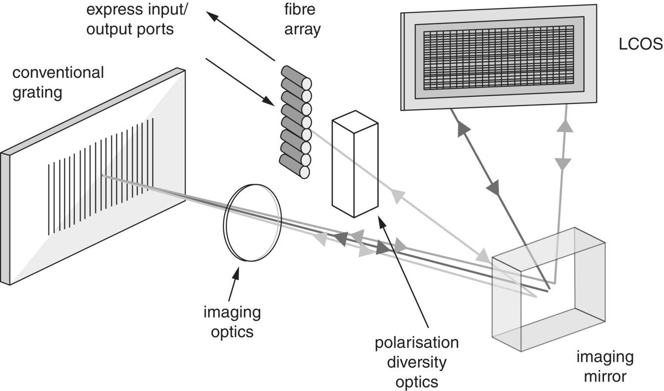
Figure 8.10 WSS architecture using LCOS beam steering.
Source: [31]/IEEE.
8.4.4.1 WSS Based on LCOS
Figure 8.10 shows a wavelength‐selective switch architecture using LCOS which provides integrated switching and optical power control in literature that include polarization diversity, control of mode [31]. In this system, the incident light from a single optical fiber is reflected from mirror and gets angularly dispersed by the grating array. This dispersed light is again reflected by the mirror and directed towards a specific portion of LCOS. This way the light of a different channel is pointed to a different section of LCOS. The same grating is used for multiplexing and demultiplexing around dynamic beam steering by LCOS, MEMS, and other elements. The wavelengths are dispersed along one dimension, and the orthogonal axis is used for port selection and possible amplitude control by beam shifts around the output fiber core center.
A multi‐pole multi‐throw (MPMT) WSS based on LCoS is presented in [69]. The MPMT function is implemented by the beam splitting with holographic phase modulation on the LCOS. It reports a 3–4.1 dB IL, maximum port crosstalk less than −20.0 dB. Both of these parameters can be further improved by the phase modulation technique. Xie et al. [70] report a Finer‐Grid WSS based on LCoS for all‐optical wavelength. To get a finer‐grid WSS, the focal length is increased here rather than decreasing the pixel size of LCoS. Based on the proposed architecture a 1 × 9 WSS was designed and tested against DPSK, QOPSK, and 16QAM signals. Authors state that both the bandwidth setting resolution and grid granularity are improved from 12.5 GHz to 6.25 GHz. Yang et al. [71] demonstrates a 1 × 12 WSS module based on a 4k LCoS device with holographic 2D beam‐steering capability and a laser‐written 3D waveguide array. It achieves an average insertion loss of −8.4 dB, crosstalk of −26.9 dB with effective passband width of 43.4 GHz.
8.5 The Future of LC switches
8.5.1 Liquid Crystal Photonic Crystal Fibers
In recent years photonic crystal fibers (PCFs) caught the attention of scientific and commercial community as new class of optical waveguides. PCFs are microstructured waveguides (in silica or polymer) with air holes located in the cladding region. In PCFs, light can be guided either by effective index mechanism related to the modified total internal reflection (TIR) or through light confinement by the photonic band gap (PBG) phenomenon. By introducing different impurities into the air holes, the propagation parameters of PCF can be tuned; in this regard LCs seem to be particularly interesting substances to infiltrate PCFs since their refractive indices can be relatively easily modified either by temperature or by an external electric field. Such a new class of micro structured fibers is known as photonic liquid crystal fibers (PLCFs).
By using the field‐dependent molecular orientation of LC, the refractive index contrast of the liquid and the fiber material can be modulated, which leads to light scattering (opaque state) or light propagation (transparent state). Thus, PLCFs allow for switching between a transparent and an opaque state. Tunable optical switches based on PLCF having a −60 dB of crosstalk, 1 dB of insertion loss with thermal tunability have been demonstrated [72]. On the other hand, PLCFs can be tuned electrically also, which allows for switching between two PBGs that depends on an ordinary refractive index of LC in OFF state and extraordinary index in ON state. This behavior offers tuning of PLCFs characterized by smooth changes in PBG positions [73, 74]. A wide and flat operating range from 600 to 1700 nm, optical switches based on PLCF with small power levels of 10 mW is reported [75], where IL is 3 dB and the CT is less than −20 dB.
8.5.2 Ring Resonators with LC
Micro‐ring resonators (mRRs) are very compact devices that can be used as routers [76] and WSS [77]. The resonant frequencies of these switches are manipulated by changing the equivalent loop length by carrier injection [78], local heating and absorption [79]. To change refractive index thermally (by introducing a heater close to the resonator) may induce problems related to power dissipation when many resonators have to be integrated in a DWDM multiplexing system. This effect is reduced by the use of silicon‐on‐insulator (SOI) wafers with an electrical tuning and nematic LCs as the waveguide side cladding, achieving a tuning range of 0.22 nm [80]. The high refractive index contrast available in SOI allows compact mRRs with low loss and high Q.
Bibliography
- 1 K.G. Vlachos, F.M. Ferreira, and S.S. Sygletos. A reconfigurable OADM architecture for high‐order regular and offset QAM based OFDM super‐channels. Journal of Lightwave Technology, 37 (16):4008–4016, 2019. doi: 10.1109/JLT.2019.2905141.
- 2 R. MacDonald, L.P. Chen, C.X. Shi, and B. Faer. Requirements of optical layer network restoration. Proceedings of Optical Fiber Communications Conference, 3:68–70, 2000. doi: 10.1109/OFC.2000.868525.
- 3 Y. Liu, E. Tangdiongga, Z. Li, S. Zhang, M.T. Hill, J.H.C. van Zantvoort, F.M. Huijskens,de H. Waardt, M.K. Smit, A.M.J. Koonen, G.D. Khoe, and H.J.S. Dorren. Ultra‐fast all‐optical signal processing: towards optical packet switching. Proceedings of SPIE: Optical Transmission, Switching and Subsystems IV, 6353:635312, 2006. doi: 10.1117/12.687147.
- 4 G.I. Papadimitriou, C. Papazoglou, and A.S. Pomoportsis. Optical switching: switch fabrics, techniques and architectures. Journal of Lightwave Technology, 21(2):372–384, 2003. doi: 10.1109/JLT.2003.808766.
- 5 S. Hardy. Liquid‐crystal technology vies for switching applications. Journal of Lightwave Technology, 44–46, 1999.
- 6 S. Chandrasekhar. Liquid Crystals (2nd edn). New York: Cambridge University Press, 1992.
- 7 N.A. Riza and S. Yuan. Low optical interchannel crosstalk, fast switching speed, polarization independent 2 × 2 fiber optic switch using ferroelectric liquid crystals. Electronics Letters, 34(13):1341–1342, 1998.
- 8 C. Vázquez, J.M.S. Pena, and A.L. Aranda. Broadband 1 × 2 polymer optical fiber switch using nematic liquid crystals. Optics Communication, 224(1–3):57–62, 2003.
- 9 F. Pain, R. Coquillé, B. Vinouze, N. Wolffer, and P. Gravey. Comparison of twisted and parallel nematic liquid crystal polarisation controllers. Application to 4 × 4 free space optical switch at 1.5 μm. Optics Communications, 139(4–6):199–204, 1997.
- 10 H. Yamazaki and M. Yamaguchi. 4 × 4 Free‐space optical switching using real‐time binary phase‐only holograms generated by a liquid‐crystal display. Optics Letters, 16(18):1415–1417, 1991.
- 11 P.C. Lallana, C. Vázquez, B. Vinouze, K. Heggarty, and D.S. Montero. Multiplexer and variable optical attenuator based on PDLC for polymer optical fiber networks. Molecular Crystals and Liquid Crystals, 502:130–142, 2008.
- 12 G.M. Zharkova, A.P. Petrov, V.N. Kovrizhina, and V.V. Syzrantsev, “Enhancing the luminophore emission of chiral polymer‐dispersed liquid crystals. Journal of Luminescence, 194:480–484, 2018. doi: 10.1016/j.jlumin.2017.10.046.
- 13 V.N. John, S.N. Varanakkottu, and S. Varghese. Flexible, ferroelectric nanoparticle doped polymer dispersed liquid crystal devices for lower switching voltage and nanoenergy generation. Optical Materials, 80:233–240, 2018. doi: 10.1016/j.optmat.2018.05.003.
- 14 E. Barsoukov and J.R. Macdonald., Impedance Spectroscopy: Theory, Experiment and Applications. New Jersey: Wiley‐Interscience, 2005.
- 15 J.M.S. Pena, I. Pérez, I. Rodríguez, C. Vázquez, V. Urruchi, X. Quintana, J. De Frutos, and J.M. Otón. Electrical model for thresholdless antiferroelectric liquid crystal cells. Ferroelectrics, 271:149–154, 2002.
- 16 I. Pérez, J.C. Torres, V. Urruchi, J.M.S. Pena, C. Vázquez, X. Quintana, and J.M. Otón. Voltage controlled square waveform generator based on a liquid crystal device. In XVII Conference on Liquid Crystals. Augustow, Poland, 2007.
- 17 C.H. Gooch and H.A. Tarry. The optical properties of twisted nematic liquid crystal structures with twist angles ≤90°. Journal of Physics D: Applied Physics, 8:1575–1584, 1975.
- 18 D.K. Yang and S.T. Wu. Fundamentals of Liquid Crystal Devices. Chichester, John Wiley, 2006.
- 19 C. Lin, H. Huang, and J. Wang. Polarization‐independent liquid‐crystal fresnel lenses based on surface‐mode switching of 90° twisted‐nematic liquid crystals. IEEE Photonics Technology Letters 22(3):137–139, 2010. doi: 10.1109/LPT.2009.2036738.
- 20 I.C. Khoo and S.T. Wu. Optics and Nonlinear Optics of Liquid Crystals. Singapore, World Scientific, 1993.
- 21 T. Choi, J. Kim, and T. Yoon, Sub‐millisecond switching of hybrid‐aligned nematic liquid crystals. Journal of Display Technology, 10(12):1088–1092, 2014. doi: 10.1109/JDT.2014.2346175.
- 22 S.P. Palto, M.I. Barnik, A.R. Geivandov, I.V. Kasyanova, and V.S. Palto. Submillisecond inverse TN bidirectional field switching mode. Journal of Display Technology, 12(10):992–999, 2016. doi: 10.1109/JDT.2016.2574929.
- 23 S.T. Lagerwall. Ferroelectric and Antiferroelectric Liquid Crystals. Weinheim: Wiley‐VCH, 1999.
- 24 N.A. Clark and S.T. Lagerwall. Submicrosecond bistable electro‐optic switching in liquid crystals. Applied Physics Letters, 36:899–901, 1980.
- 25 J.R. Moore and A.R.L. Travis. PSpice electronic model of a ferroelectric liquid crystal cell. IEEE Proceedings – Optoelectronics, 146(5):231–236, 1999.
- 26 G. Moddel, K.M. Johnson, W. Li, R.A. Rice, L.A. Pagano‐Stauffer, and M.A. Handschy. High‐speed binary optically addressed spatial light modulators. Applied Physics Letters, 55:537–639, 1989.
- 27 I. Underwood, D.G. Vass, and R.M. Sillitto. Evaluation of an nMOS VLSI array for an adaptive liquid‐crystal spatial light modulator. IEE Proceedings, Part J: Optoelectronics, 133:77–83, 1986.
- 28 A. Lelah, B. Vinouze, G. Martel, T. Perez‐Segovia, P. Geoffroy, J.P. Laval, P. Jayet, P. Senn, P. Gravey, N. Wolffer, W. Lever, and A. Tan. A CMOS VLSI pilot and support chip for a liquid crystal on silicon 8 × 8 optical cross‐connect. Proceedings of SPIE: Wave Optics and VLSI Photonic Devices for Information Processing, 4435:173–183, 2001.
- 29 Huang Y, Liao E, Chen R, Wu S‐T. Liquid‐crystal‐on‐silicon for augmented reality displays. Applied Sciences, 8(12):2366, 2018. doi: 10.3390/app8122366.
- 30 W. Hossack, E. Theofanidou, J. Crain, K. Heggarty, and M. Birch. High‐speed holographic optical tweezers using a ferroelectric liquid crystal microdisplay. Optics Express, 11:2053–2059, 2003.
- 31 G. Baxter et al. Highly programmable wavelength selective switch based on liquid crystal on silicon switching elements. 2006 Optical Fiber Communication Conference and the National Fiber‐Optic Engineers Conference, 2006. doi: 10.1109/OFC.2006.215365.
- 32 K. Heggarty, B. Fracasso, C. Letort, J.L. de Bougrenet de la Tocnaye, M. Birch, and D. Krüerke. Silicon backplane ferroelectric liquid crystal spatial light modulator for uses within an optical telecommunications environment. Ferroelectrics, 312:39–55, 2003.
- 33 C. Yu, X. Jiang, S. Horiguchi, and M. Quo. Overall blocking behavior analysis of general banyan‐based optical switching networks. IEEE Transactions on Parallel and Distributed Systems, 17(9):1037–1047, 2006.
- 34 K. Hogari, K. Noguchi, and T. Matsumoto. Two‐dimensional multichannel optical switch. Applied Optics, 30(23):3277–3278, 1991.
- 35 S. Fukushima, T. Kurokawa, and M. Ohno. Real‐time hologram construction and reconstruction using a high resolution SLM. Applied Physics Letters, 58:787–789, 1991.
- 36 R.E. Wagner and J. Cheng. Electrically controlled optical switch for multimode fiber applications. Applied Optics, 19(17):2921–2925, 1980.
- 37 L.R. McAdams, R.N. McRuer, and J.W. Goodman. Liquid crystal optical routing switch. Applied Optics, 29(9):1304–1307, 1990.
- 38 C. Vázquez, J.M.S. Pena, and A.L. Aranda. Broadband 1 × 2 polymer optical fiber switches using nematic liquid crystals. Optics Communications, 224(1–3):57–62, 2003. doi: 10.1016/S0030‐4018(03)01716‐4.
- 39 S. Sumriddetchkajorn and N.A. Riza. Fiber‐conectorized multiwavelength 2 × 2 switch structure using a fiber loop mirror. Optics Communications, 175:89–95, 2000.
- 40 R.A. Soref. Low‐cross‐talk 2 × 2 optical switch. Optics Letters, 6(6):275–277, 1981.
- 41 R.A. Soref and D.H. McMahon. Calcite 2 × 2 optical bypass switch controlled by liquid‐crystal cells. Optics Letters, 7(4):186–188, 1982.
- 42 L.R. McAdams, R.N. McRuer, and J.W. Goodman. Liquid crystal optical routing switch. Applied Optics, 29(9):1304–1307, 1990.
- 43 G.J. Grimes, L.L. Blyler, A.L. Larson, and S.E. Farleigh. A plastic optical fiber based photonic switch. Proceedings of SPIE: Plastic Optical Fibers, 1592:139–149, 1991.
- 44 Y. Fujii. Low‐crosstalk 2 × 2 optical switch composed of twisted nematic liquid crystal cells. IEEE Photonics Technology Letters, 5(6):715–718, 1993.
- 45 N.A. Riza and S. Yuan. Reconfigurable wavelength add‐drop filtering based on a banyan network topology and ferroelectric liquid crystal fiber‐optic switch. Journal of Lightwave Technology, 17(9):1575–1584, 1999.
- 46 C. Vázquez, J.M.S. Pena, and A.L. Aranda. Broadband 1 × 2 polymer optical fiber switch using nematic liquid crystals. Optics Communications, 224(1–3):57–62, 2003.
- 47 P.C. Lallana, C. Vázquez, J.M.S. Pena, and R. Vergaz. Reconfigurable optical multiplexer based on liquid crystals for polymer optical fiber networks. Opto‐Electronics Review, 14(4):311–318, 2006.
- 48 P.C. Lallana, C. Vázquez, D.S. Montero, K. Heggarty, and B. Vinouze. Dual 3 × 1 multiplexer for POF networks. Proceedings of International Conference on Plastic Optical Fibers. Torino. 33–36, 2007.
- 49 J. Yang, X. Su, X. Liu, X. He, and J. Lan. Design of polarisation‐independent bidirectional 2 × 2 optical switch. Journal of Modern Optics, 55(7):1051–1063, 2008.
- 50 X. Hu, O. Hadeler, and H.J. Coles. Ferroelectric liquid crystal mixture integrated into optical waveguides. Journal of Lightwave Technology, 30(7):938–943, 2012. doi: 10.1109/JLT.2012.2184738.
- 51 F. Zhang, H.‐H. Chou, and W.A. Crossland. PLZT‐based shutters for free‐space optical fiber switching. IEEE Photonics Journal, 8(1):7800512, 2016. doi: 10.1109/JPHOT.2015.2511090.
- 52 T. Li, Q. Chen, and X. Zhang. Optofluidic planar optical cross‐connect using nematic liquid‐crystal waveguides. IEEE Photonics Journal, 10(4):6601417, 2018. doi: 10.1109/JPHOT.2018.2853759.
- 53 J. Qi, L. Li, and G. Crawford. Switchable infrared reflectors fabricated in polymer‐dispersed liquid crystals. OFC 2003 Optical Fiber Communications Conference, 2003, 43–44. doi: 10.1109/OFC.2003.1247477.
- 54 D. Bosc, C. Trubert, B. Vinouze, and M. Guilbert. Validation of a scattering state model for liquid crystal polymer composites. Applied Physics Letters, 68:2489–2490, 1996.
- 55 B. Fracasso, J.L. de Bougrenet de la Tocnaye, L. Noirie, M. Razzak, and E. Danniel. Performance assessment of a liquid crystal multichannel photonic space‐switch. Photonics in Switching (Technical Digest), 24–26, 2001.
- 56 C. Letort, B. Vinouze, and B. Fracasso. Design and fabrication of a high‐density 2D fiber array for holographic switching applications. Optical Engineering, 47(4):045401‐1–045401‐9, 2008.
- 57 W. Klaus, S. Shinomo, M. Ide, M. Tsuchiya, and T. Kamiya. Efficient beam deflector with a blazed liquid crystal phase grating. Proc Opt Comp. Sendai. 28–29, 1996.
- 58 J.W. Goodman and A.M. Silvestri. Some effects of Fourier‐domain phase quantization. IBM Journal of Research and Development, 14:478, 1970.
- 59 N. Wolffer, B. Vinouze, R. Lever, and P. Gravey. 8 × 8 holographic liquid crystal switch. Proceedings of SPIE: European Conference on Optical Communication, III, 2000:275–276, 2000.
- 60 A. Tan, A. Bakoba, N. Wolffer, B. Vinouze, and P. Gravey. Improvement of response times of electrically addressed nematic liquid crystal blazed gratings. Proceedings of SPIE: European Conference on Optical Communication, 2000, 4089: 208, 2000.
- 61 M. Vasilyev, I. Tomkos, J.K. Rhee, M. Mehendale, B.S. Hallock, B.K. Szalabofka, M. Williams, S. Tsuda, and M. Sharma. Broadcast‐and‐select OADM in 80 × 10, 7 Gbit/s ultra‐longhaul networks. IEEE Photonics Technology Letters, 15:332–334, 2003.
- 62 J.K. Rhee, F. Garcia, A. Ellis, B. Hallock, T. Kennedy, T. Lackey, R.G. Lindquist, J.P. Kondis, B.A. Scott, J.M. Harris, D. Wolf, and M. Dugan. Variable pass‐band optical add‐drop multiplexer using wavelength selective switch. Proceedings of European Conference on Optical Communication, 2001. Amsterdam. 550–551, 2001.
- 63 P. Bonenfant and M. Loyd. OFC 2003 workshop on wavelength selective switching based optical networks. IEEE Journal of Lightwave Technology, 22(1):305–309, 2004.
- 64 Yunshu Gao, Xiao Chen, Genxiang Chen, Ying Chen, Qiao Chen, Feng Xiao, Yiquan Wang, 1 × 25 LCOS‐based wavelength selective switch with flexible passbands and channel selection, Optical Fiber Technology, 45:29–34, 2018. doi 10.1016/j.yofte.2018.05.008.
- 65 D.M. Marom, D.T. Neilson, D.S. Greywall, C.S. Pai, N.R. Basavanhally, V.A. Aksyuk, D.O. Lopez, F. Pardo, M.E. Simon, Y. Low, P. Koodner, and C.A. Bolle. Wavelength‐selective 1 × K switches using free‐space optics and MEMS micromirrors: theory, design and implementation. IEEE Journal of Lightwave Technology, 23(4):1620–1630, 2005.
- 66 J.P. Heritage, A.M. Weiner, and N.R. Thurston. Picosecond pulse shaping by spectral phase and amplitude manipulation. Optics Letters, 10:609–611, 1985.
- 67 J.S. Patel and Y. Silberberg. Liquid‐crystal and grating‐based multiple wavelength cross‐connect switch. IEEE Photonics Technology Letters, 7(5):514–516, 1995.
- 68 H. Asakura et al. A 200‐GHz spacing, 17‐channel, 1 × 2 wavelength selective switch using a silicon arrayed‐waveguide grating with loopback. In 2015 International Conference on Photonics in Switching (PS), 52–54, 2015. doi: 10.1109/PS.2015.7328950.
- 69 K. Yamaguchi, Y. Ikuma, M. Nakajima, K. Suzuki, M. Itoh, and T. Hashimoto. M × N wavelength selective switches using beam splitting by space light modulators. IEEE Photonics Journal, 8(2): 0600809, 2016. doi: 10.1109/JPHOT.2016.2527705.
- 70 D. Xie et al. LCoS‐based wavelength‐selective switch for future finer‐grid elastic optical networks capable of all‐optical wavelength conversion. IEEE Photonics Journal, 9(2):7101212, 2017. doi: 10.1109/JPHOT.2017.2671436.
- 71 H. Yang et al. 24 [1 × 12] wavelength selective switches integrated on a single 4k LCoS device. Journal of Lightwave Technology 39(4):1033–1039, 2021. doi: 10.1109/JLT.2020.3002716.
- 72 T.T. Larsen, A. Bjarklev, D.H. Sparre, and J. Broeng. Optical devices based on liquid crystal photonic bandgap fibres. Optics Express, 11(20):2589–2596, 2003.
- 73 T.R. Wolinski, K. Szaniawska, S. Ertman, P. Lesiak, and A.W. Domanski. Photonic liquid crystal fibers: new merging opportunities. In Proceedings of the Symposium on Photonics Technologies for 7th Framework Program, 95–99, 2006.
- 74 M.W. Haakestad, T.T. Alkeskjold, M.D. Nielsen, L. Scolari, J. Riishede, H.E. Engan, and A. Bjarklev. Electrically tunable photonic bandgap guidance in a liquid‐crystal‐filled photonic crystal fiber. IEEE Photonics Technology Letters, 17:819–821, 2005.
- 75 J. Tuominen, H. Hoffren, and H. Ludvigsen. All‐optical switch based on liquid‐crystal infiltrated photonic bandgap fiber in transverse configuration. Journal of the European Optical Society, Rapid Publications, 2, 2007.
- 76 C. Vázquez, S.E. Vargas, and J.M.S. Pena. Design and tolerance analysis of arouter using an amplified ring resonator and Bragg gratings. Applied Optics, 39(12):1934–1940, 2000.
- 77 J.E. Heebner and R.W. Boyd. Enhanced all‐optical switching by use of a nonlinear fiber ring resonator. Optics Letters, 24(12):847–849, 1999.
- 78 K. Djordjev, S. Choi, S. Chou, and P. Dapkus. Microdisk tunable resonant filters and switches. IEEE Photonics Technology Letters, 14(6):828–830, 2002.
- 79 B.E. Little, H.A. Haus, J.S. Foresi, L.C. Kimerling, E.P. Ippen, and D.J. Ripin. Wavelength switching and routing using absorption and resonance. IEEE Photonics Technology Letter, 10(6):816–818, 1998.
- 80 B. Maune, R. Lawson, C. Gunn, A. Scherer, and L. Dalton. Electrically tunable ring resonators incorporating nematic liquid crystals as cladding layers. Applied Physics Letters, 83(23):4689–4691, 2003.