
7
SOA‐based Optical Switches
Xuwei Xue1, Shanguo Huang1, Bingli Guo1, and Nicola Calabretta2
1 State Key Laboratory of Information Photonics and Optical Communications (IPOC), Beijing University of Posts and Telecommunications, Beijing, China
2 Eindhoven University of Technology, Eindhoven, Netherlands
7.1 Introduction
With the continuous advances in the experiments and development of the optical components and subsystems constituting the physical layer, capacity and speed in fiber‐optic communication networks have increased over the past decades. Technologies of component miniaturization and integration that continue to improve the performance in the network while maintaining economic feasibility are of paramount importance. To achieve such extremely high data rates, utilizing semiconductor optical amplifiers (SOAs) as the key element in optical communication is a feasible scheme. Amplification of optical signals is not the only application SOAs are limited to. It is also validated performing as a significant element in high‐speed optical switching, wavelength conversion, optical regeneration, demultiplexing, all‐optical triodes, and all‐optical logic doors. Benefits of SOAs are well‐known including half‐rack size, wide gain band, integration compared to the Erbium‐doped Optical Fiber Amplifier (EDFA), especially their fast switching speed and the capability to modulate pulse signals with a high extinction ratio. However, the high coupling loss with optical fiber, mixed with the considerable noise and crosstalk which are sensitive to ambient temperature, is a crucial influence factor introduced by SOAs. The purpose of this chapter is to present metrics illustrations, design criteria, and performance enhancements for SOA‐based switches. After our preface in this chapter, Section 7.2 will describe the structure of SOA. Subsequently, we will expound design criteria of SOA‐based switches in Section 7.3. Moreover, improvements on SOA‐based switches will be generalized in Section 7.4. In Section 7.5 and Section 7.6, the networks employing SOA‐based switches, discussion, and future work will be summarized and proposed.
7.2 SOA Structure
The versatile structure of the SOA is comprised of an active region encompassed with passive cladding material, similar to the semiconductor laser. As depicted in Figure 7.1, in other words, the active region is the gain region, which is made of semiconductor materials such as INP. The main difference from semiconductor lasers is an anti‐reflective coating to prevent reflection of the SOA end face and eliminate the resonator effect. A little clue, anti‐reflective coating is arranged in the end face of a single or multilayer dielectric layer.

Figure 7.1 The amplifying process of SOA.
There are four types of SOAs: Fabry–Pérot SOA (FP‐SOA), gain‐clamped SOA (GC‐SOA), traveling‐wave SOA (TW‐SOA), and quantum dot SOA (QD‐SOA), where the third due to less or no internal reflection versus a large optical bandwidth and low polarization sensitivity is widely used [1].
7.2.1 Active Region
As it is described, the active region is the place where incident light is amplified. It is the result of the stimulated emission which occurred posteriorly the population inversion (E2>E1). Actually, the process in the amplification begins with the injected electric currents. Meanwhile, these electrons in the heterojunction will be moved by the electric field to form a pair of electron holes, and when the incident light comes, the electrons will lose energy as photons and return to their ground state. Generally speaking, the active region is an attractive slide. Your children are raised by you (injection current), and they will slip when the wind (incident light) blows across the slide. Subsequently, following the children, it will generate the same frequency “wind” to enlarge the initial wind. The structure of polarization‐insensitive SOA is shown in Figure 7.2.
Figure 7.2 The structure of polarization‐insensitive SOA.

Figure 7.3 Different active region of SOAs: (a) bulk material, (b) quantum well, (c) quantum wire, (d) quantum dots.
In the SOA, the active region can be in form of bulk, quantum wells (QWs), quantum wire, and quantum dot [2]. As depicted in Figure 7.3(a), the bulk gain media density of state (DOS) increases as a parabola with the rising energy. With the improving doping technique and innovative structures, the performance of SOA keeps the momentum developing from quantum wells and quantum wires to quantum dots. The quantum well structures are constrained in one dimension, usually in the epitaxial growth direction. Figure 7.3(b) illustrates the correlation between the DOS and energy in a stepwise growing. Diverse with the quantum wells, carriers in quantum wires can only move freely in one direction due to the quantum constraints of two dimensions. Meanwhile, the delta‐like correlativity of two factors is depicted in Figure 7.3(c). Furthermore, with the best property, the structure of quantum dots is similar to the atoms, where electrons and holes are quantum‐restricted in three directions. The impulse line along with the energy level is shown in Figure 7.3(d).
7.2.2 Inter‐Band Versus Intra‐Band Transition
Based on the position of the electron transition, the excitation emission within the SOA is divided into two classes: inter‐band and intra‐band. Inter‐band variation refers to the transfer of carriers in conduction and valence bands, as shown in Figure 7.4. When there is no injection current, most of the electrons are in the valence band, only a few electrons are transferred in it. Nevertheless, with the injection of current, the electrons drift to the conduction band while the electron density of the conduction band increases and holes in the valance band before the number of population inversion. They will spontaneously recombine with holes in sub‐nanosecond time scales from the conduction band to the valence band, as well as releasing the energy by emitting photons. Moreover, the lifetime of the non‐equilibrium free carrier is reduced to picosecond magnitude as a result of the stimulated emission process. Within the procedure of current injection, population inversion will occur between valence band and higher conduction band levels when the injection is beyond a threshold [3].
Because of the continuous intra‐band energy levels, the injected hot carriers can quickly compensate for the reduced carriers due to stimulated emission by relaxation. The time of supplement is approximately 50 femtosecond or higher, much faster than the picosecond time scales of inter‐band mechanisms. Hence, carriers in the whole active region are rapidly depleted while it ensues uniform gain saturation formed.
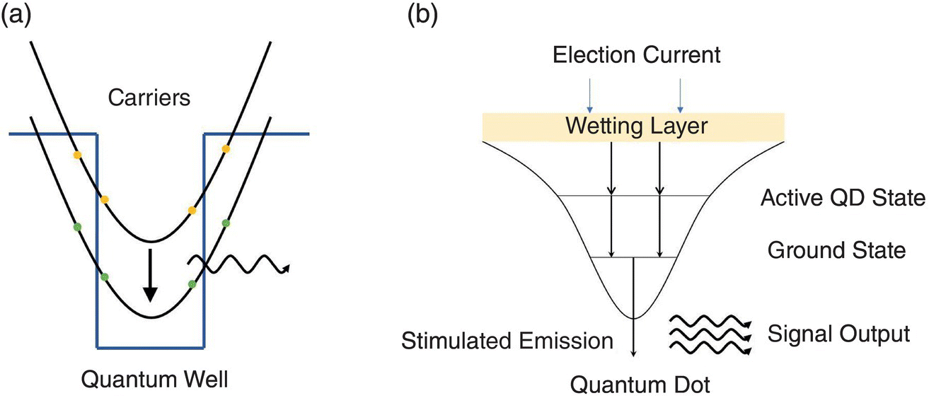
Figure 7.4 Intra‐band and inter‐band transition and stimulated emission of (a) QWs and (b) QDs.
The aforementioned intra‐band process is the ideal transition and recombination state of carriers, emitting phonons, however, there is an atypical non‐radiation process called Auger recombination. It is a significant phenomenon with the recombination of electron‐hole, where the excess energy from it is transferred to electrons or holes. Subsequently, the energy is excited to higher energy states within the same band instead of giving off photons (the radiative process). With high carrier or current density, the Auger recombination may play a crucial role in the resultant processing of gain droop.
7.2.3 Transparency Threshold
Transparency threshold in the SOA is the minimal current density of the gain media that the SOA with no amplification and absorption. Hence, if the injection current lies in or beyond the threshold current density, it can be described in a transparent state. The relationship between optical gain of SOA with the photon energy and the carrier density is quite complex. Whereas, we can simplify the whole relation in brief equations. ItA is the threshold current in active region expressed in Equation 7.1:
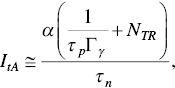
where α is the electron charge multiplied by the volume of the active region, τp is the photon’s lifetime, Γ is the confinement factor, γ is the differential gain coefficient multiplied with the group velocity, NTR is the carrier density at the transparency condition, τn is the photon’s lifetime. S0 is the steady‐state photon density above ITR [4], as depicted in Equation 7.2.

where I0 depicts the current injection of the whole process into the SOA, meanwhile, Ith equals ItA plus IF, which is the leakage current. On the basis of the relationship between the density of states and the energy of the injected current in Figure 2.3, taking the quantum wells and the bulk materials as a comparison, it is effortlessly ascertained that there is a lower transparency current achieved in QW materials compared to bulk materials. In other words, it achieves higher concentration of carriers in the same current with a smaller volume by the enhanced confinement of the electrons/holes. Meanwhile, the size of conduction and valence band offset determine the efficacy of the constraint. To postpone the saturation point, a deeper QW is a convenient scheme, whereas the deeper wells fabricate other problems such as non‐uniformity in carrier distribution across multiple wells. In the transparent pattern, moreover, several all‐optical switching devices implement the on/off function by virtue of the transparency with nonlinearity. The concept and application of gain nonlinearity will be discussed in the next dot [5].
7.2.4 Gain Nonlinearity
The value of amplifier gain G is a significant parameter in elimination for the performance of SOAs. It is defined as the Equation 7.3:

G is increasing with device length, in turn with the reduction, when the internal gain is limited by gain saturation. Where gm, α, and L are the material gain coefficient, the effective absorption coefficient of the material, and amplifier length respectively. In practice, the signal distortions are possibly introduced by SOA gain saturation, which manifests as the transmission quality degradation. In a feasible scheme, the adequate saturation output power is required at a high state to alleviate the influences of these distortions. The optical gain of SOA is defined in another form of the carrier density N by Equation 7.4:
where Γ is the confinement factor, a is the differential gain coefficient, Nt is the carrier density at transparency, and L denotes the SOA length. Therefore, the optical gain of SOA can be translated into the factor controlled by the carrier density generation. With the nonlinearities of SOAs, the main types exploited in all‐optical networks are cross‐gain modulation (XGM), cross‐phase modulation (XPM), self‐phase modulation (SPM), and four‐wave mixing (FWM) [1]. The saturation of SOAs is the basic requirement of XGM, which is, hence, converting the signal into another wavelength. In the comparison between XPM and XGM, the biggest difference may arise with the former where refractive index of the active region in SOA is not constant, which is relative to the carrier density and the material gain. The gain nonlinearity is always in used with the SOA‐MZI configuration while the SPM compensates the pulse broadening after the transition in fibers. Additionally, FWM with the strong pump for the wavelength conversion can offer the phase and amplitude information of the signals whilst the weak probe signal is injected.
7.2.5 Polarization‐Insensitive SOA
The gain polarization sensitivity of SOA can be explained in two ways: i) the different amplification for transverse electric (TE) polarization and for transverse magnetic (TM) polarization in waveguides even though the confinement to the active layer is comparable for the two states and ii) the anisotropy of the light‐matter interaction in a quantum well [6]. The amplification of TE and TM modes is different, which is due to the rectangular shape and the crystal structure of the active region. It makes gain coefficient (g) and confinement factor (Γ) dependent on polarization.
There are many scenarios for fabricating polarization‐insensitive SOAs. For example, the SOA may provide approximately polarization‐insensitive characteristics with the intrinsic polarization‐sensitive designs. It uses two identical amplifiers in cascades, where the difference of both amplifiers is the 90° included angle between them. Additionally, there are also two parallel amplifiers deploying for the two polarization directions. Furthermore, polarizing beam splitters (PBSs) are simultaneously deployed for these amplifiers front and back [7]. Besides, the polarization diversity circuit based (PDC‐based) SOAs are several polarization‐insensitive devices. One of the typical PDC‐based SOA structures can be divided into three components: polarization‐sensitive SOAs as mentioned before, half wave plates (HWPs), and PBSs, while the number of them is the same as mentioned before in two [8]. The PBS will split the incident signal into TE and TM components. Furthermore, another scheme is the use of a Faraday rotator between the device and the reflecting mirror with a bidirectional amplifier. Additionally, the balance of the gain between TE and TM mode is another feasible method. There is the introduction of tensile strain into the active layer to implement the envision. However, the requirement is an obstacle to the high‐precision control of the thickness and the strain of the active layer. Meanwhile, the crystalline reliability of the active layer is also influenced with a mass of strain. Besides, the deployment of the polarization‐dependent loss (PDL) is another approach. TE and TM polarized signal can be amplified with the application of one polarization‐insensitive SOA. Nevertheless, inasmuch as the fiber has the predetermined length of the PDL unit, it introduces extra loss and the difficulty of integrating with other devices.
In the experiment of multiple‐quantum‐well structures of SOAs, the TE‐polarized signal exceeds TM‐polarized signal in the optical gain as observed in the use of typical self‐assembled InAs/GaAs QDs, where the amplitude of output signal is affected with detrimental fluctuations [9]. Bulk and MQW achieve polarization insensitivity through choice of nearly square cross‐sections of the active layers.
7.2.6 Noise in SOA
With the deficiency of analytical architecture of noise in the SOAs, we merely calculate the noise in detection or in our mathematical models [10]. To measure the noise, we will ascertain the definition of relative factors and relations. Firstly, Optical Signal to Noise Ratio (OSNR) is a key to represent the signal quality effected with the noise generated in long transmitted distance like amplified spontaneous emission (ASE) noise etc. This is expressed in a general formula in Equation 7.5:
where S is the signal power and N is the noise power. Both of them are in watts or milliwatts. The higher ratio value of them manifests the better signal integrity after transforming the overall system, whose measurements are defined in IEC 61282‐12 / b‐IEC 61280‐2‐9 standards [11], illustrated in Equation 7.6:
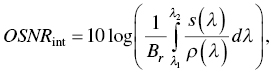
where s(λ) is time‐averaged signal spectral power density without including ASE. Additionally, ρ(λ) is the ASE spectral power density which is independent of polarization, both of which expressed in W/nm. Br is the reference bandwidth expressed in nm with the default value 0.1 nm if there is no other statement [12]. To accommodate the amplification between the signal and noise, the OSNR degradation is expressed in terms of noise factor (NF) dB as Equation 7.7:
where G is the optical power gain of the device. Posteriorly, in general, with the higher driving current or pumping input power in the SOA, the noise will increase parabolically in the SOAs [13].
Moreover, electron density fluctuation in the SOA affects the noise characteristics in the lower frequency region than 100 MHz. Hence, corresponding to an inverse value of the S/N ratio, the relative intensity noise (RIN), which is supposed to be higher after passing through the SOAs, will reach a lower level than the RIN of the incident light when there is high optical input power beneath the 100MHz. Additionally, the RIN in the SOA including the ASE for operation is higher than RIN in other amplifiers like EDFAs with low optical input power, which synchronously get higher phase noise and frequency noise in the SOAs because of the larger optical absorption.
7.3 Design Criteria of SOA‐Based Switch
Based on the different applications of SOA as the switch, differences should be highlighted in them. There are several SOA‐based switches, for example, Terahertz Optical Asymmetric Demultiplexer (TOAD), the switches derived from the structure of Mach–Zehnder interferometer (MZI) like Colliding Pulse Mach–Zehnder (CPMZ) and the variation Symmetric Mach–Zehnder (SMZ) etc. The structure of them is illustrated in Figure 7.5. Furthermore, different features of SOA can be divided the switches in two categories, on the basis of the linear (gating) or nonlinear (wavelength conversion) operation task. Besides, all of them will make corresponding fine adjustments according to different functions. Briefly described, the temporal window of TOAD is controlled with the SOA relative position of the midpoint. Control pulses will introduce a differential phase shift in the Mach–Zehnder‐based switches. Moreover, reduced current threshold with low confinement factors in the gating applications and the long active regions with high confinement factors for wavelength conversion are also considered.
7.3.1 Effect of Doping on Gain Dynamics
With the different doping techniques, it is categorized in p‐doped (hole‐doped) barriers and n‐doped (electron‐doped) barriers. In their applications, with the balk of a certain level, the unsaturated optical gain can be greatly enhanced through p‐type doping. Nevertheless, increasing p‐type concentration will be associated with saturation density declining and an increase in the transparency current. In turn, the n‐type doping used can possibly increase the saturation density and enhance the linearity of the SOA [14]. Not merely of these effects, the n‐doping strongly influences the transparency level. Meanwhile, the amplifier noise enhancement factor nsp is more effectively reduced by the n‐doping than p‐doping at a given excitation level [15], as illustrated in Figure 7.6 [16]. Meantime, there are various materials doped in the system. For instance, InAs/GaAs is the p‐doping system, simultaneously, GaAs (AlGaAs) is the n‐doping.
Above all, we will introduce the effect of p‐doping on gain dynamics. Basically, the p‐doping manifests the temperature insensitive threshold current, linewidth enhancement factor, high peak modal gain, and high modulation bandwidth [16]. Actually, the basic idea of p‐doping is the way to fill the QD hole states. In a p‐doped device, despite the occupation of electrons only aggregated at the ground state (GS) due to the low injection of carriers, the built‐in hole reservoir grants the occurrence of fast hole‐hole scattering. Subsequently, the instant in the removed implementation of a GS electron‐hole pair controlled by pump impulse, electrons will recover, while the unsaturated gain is enhanced. Nevertheless, in the p‐doped InAs/GaAs QD amplifiers, such gain dynamics will be followed by slow electron dynamics on the 100 ps scale due to the lack of electron carriers in the higher energy states. In the experiment of Cesari et al. [17], it measures the ultrafast gain dynamics of the GS transition with the emission of 1.3 μm InAs/GaAs QD amplifiers in an electrical pump at room temperature. In fabrication under same conditions, the slower gain dynamics are observed in p‐doped amplifiers compared with the undoped devices at the operation of the identical gain. In fact, the reduction of the excited‐state electrons reservoir contributes to slower gain dynamics in p‐doped quantum dot devices, which confines the recovery of the electron ground‐state occupation mediated by intra‐dot carrier‐carrier scattering. Thus, it demonstrates that the benefits of p‐doping are uncertain for the applications of ultrafast optoelectronics [16].
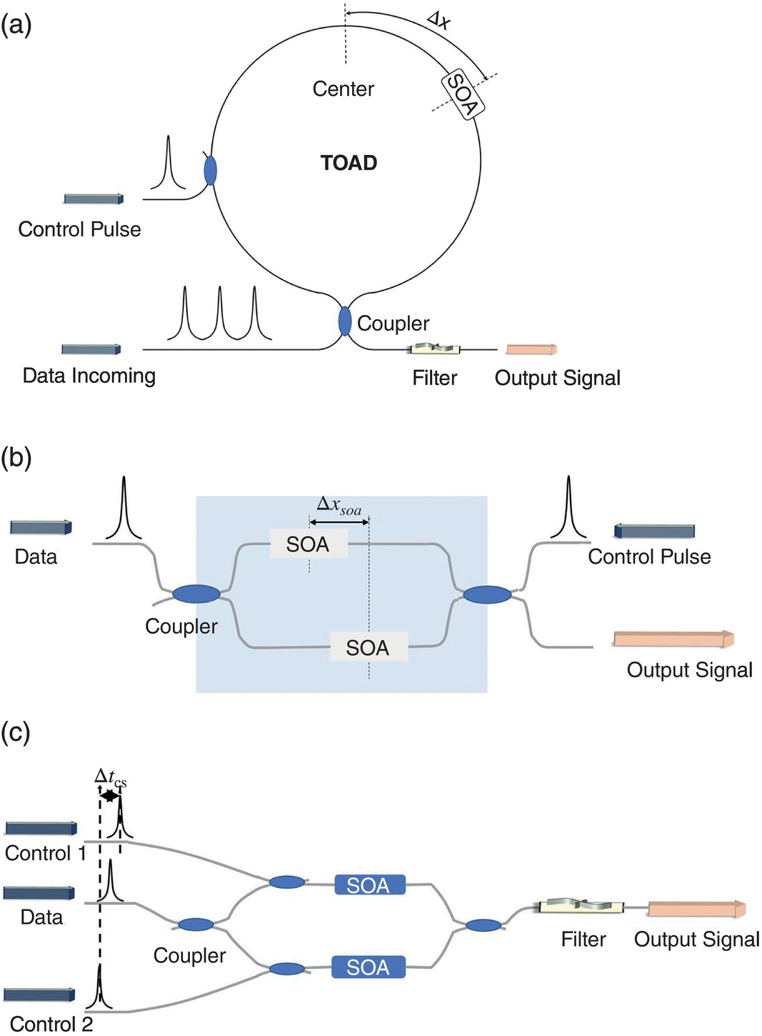
Figure 7.5 The structure of (a) TOAD, (b) CPMZ, (c) SMZ.

Figure 7.6 The differences between various doped material
With the investigation of quantum dot vertical cavity semiconductor optical amplifier (QD‐VCSOA), it is depicted that under the WL pumping operation, the gain and saturation threshold will increase with the acquisition of gain recovery dynamics [18].
7.3.2 Gain Dynamic for SOA
In the widest applications of high‐speed systems, SOAs with faster gain dynamics are the best scheme in the expected future. To accurately describe the dynamic gain in SOA, we similarly use pump‐probe spectroscopy technology to characterize the dynamic gain performance. In most experiments, the gain dynamic can be represented in the electron density, the recovery time, and the recombination time of the electron‐hole pairs etc. On the basis of these characteristic analysis methods, the difference on gain dynamics between the configuration of co‐propagating and counter‐propagating for SOAs will be described briefly, and not merely this, but the different gain dynamics between the form of materials, the bulk, quantum well, and quantum dot amplifiers will be also organized in order subsequently.
The basic rate equation can be written in the same way as the propagation Equation 7.8:
where ![]() and
and ![]() are the power of the forward‐ and backward‐propagating ASE beam, respectively, λase is a parameter only for the units to analyze, and σ is the cross‐section of the gain region. I is the bias current, gase is modal gain of the ASE. Meanwhile, the effective value ηI is the efficiency coefficient of the injection of carriers, V is the volume of the active region, R(n) is the recombination rate totally, q is the constant of electron charge, and g is the modal gain. Meantime, P is the value of power and λsig is the wavelength of the input signal [19].
are the power of the forward‐ and backward‐propagating ASE beam, respectively, λase is a parameter only for the units to analyze, and σ is the cross‐section of the gain region. I is the bias current, gase is modal gain of the ASE. Meanwhile, the effective value ηI is the efficiency coefficient of the injection of carriers, V is the volume of the active region, R(n) is the recombination rate totally, q is the constant of electron charge, and g is the modal gain. Meantime, P is the value of power and λsig is the wavelength of the input signal [19].
Based on this equation, according to experimental results, in the co‐propagating configuration, it is observed that the gain for a bias current and input power before the threshold can be evaluated with the present overshoot in the gain recovery. Nevertheless, with the input power constantly increasing, another turning point brings the disappearance of the overshoot because of the recovery time rising. But with the differently injected wavelength, the performance and the effects will demonstrate distinctive properties. Moreover, in the counter‐propagating configuration, the increase of injected power induces a considerable reduction in the recovery time. If the wavelength matches to the gain region, the improvement of counter‐propagating will reduce as compared to the co‐propagating scheme for high‐injected power. Altogether, in the gain recovery, with the comparison to the two configurations in the same injected power, it is obvious that the counter‐propagating with the overshoot is present, which is the cause of the carrier dynamics.
7.3.2.1 Bulk‐Active Regions
In the experimental simulations, the bulk‐active region should be able to achieve significantly 40 ps gain recovery time. Utilizing butt‐joint growth (BJG) for bulk‐active region definition, the bandgap of the bulk‐active layer is 1565 nm and the layer thickness is 180 nm. The bulk‐active region presents high confinement, which shows the excellent performance at 40 Gb/s [20]. Meantime, in order to use the SOA intra‐band fast dynamics for high‐speed applications, the slow gain compression should be kept to the smallest value possible for the slow dynamics of it. Furthermore, in the general of bulk‐SOAs, the fast gain recovery time increases with increasing current and pulse energy [21]. Nevertheless, the time is slightly independent on the active region length. With varying the pulse energy, it is observed with the values of gain recovery time reducing. In fact, the different polarization waves of bulk SOAs are also containing the distinct gain recovery time [22]. In the TM axis, longer carrier recovery time is due to the fact that for a bulk tensile strained device there are more TM transitions than TE transitions because of the shifting of the sub‐bands in the valence band. In this situation, the light holes giving rise to the TM transitions are favored.
7.3.2.2 Quantum Well/Multi‐Quantum Well (MQW) Active Regions
The applications of MQW structures are related to the predictions of differential gain enhancement and of current threshold reduction with a high differential gain which has a positive impact on the performances on SOAs [23]. In MQW, there is also an overshoot occurring. At high current bias, in the region of the SOA where carriers are strongly depleted, as a sequence, the injection rate becomes slightly faster than the cumulative recombination rates. Moreover, another characteristic of MQW‐SOAs will appear, the non‐uniform distribution of carriers, under strong optical excitation. As a comparison, the tendency of results in experiment are similar. It indicates the QWs exchanges the necessary carriers to support stimulated recombination, creating a carrier flux toward the middle portion of the structure. The recombination procedures become faster as carrier density increasing to higher values, consequently, the smaller gain recovery time compared the MQWs, 170 ps. These recovery times are directly related to the maximum repetition rate at the performance of the amplifier in wavelength multiplexing.
7.3.2.3 Quantum Dots
In semiconductor quantum dot optical amplifiers, some researches have proposed some quantitative analysis methods. Furthermore, it is very different in the QD, and carrier dynamics in the QDs are critical for distinguishing these SOAs [24]. In these experiments, fast gain recovery (~100 fs) dynamics have been preciously observed in an InAs‐InGaAs QD active waveguide [25]. To describe the relations in QD‐SOA in details, the factors influenced the gain dynamics are exhibited below. The DOS for the QD, ρG, is extrapolated in Equation 7.9:
where ![]() is a parameter of the influence of FWHM in the GS transition, the phenomenon manifests as inhomogeneous broadening. n1 is the number of QD layers, decided after the fabrication in the device. D3D is the density of 3D dot in a single dot layer versus the volume V. Moreover, εG is the degeneracy of the GS of a single dot, which is constant 2 because of spin. With the approximation to the GS transition, the majority of inhomogeneous broadening is arising from the same electron states in assumption.
is a parameter of the influence of FWHM in the GS transition, the phenomenon manifests as inhomogeneous broadening. n1 is the number of QD layers, decided after the fabrication in the device. D3D is the density of 3D dot in a single dot layer versus the volume V. Moreover, εG is the degeneracy of the GS of a single dot, which is constant 2 because of spin. With the approximation to the GS transition, the majority of inhomogeneous broadening is arising from the same electron states in assumption.
The rate equations indicating the time revolution of the electrons are Equations 7.10 and 7.11:

where I is the injected current, and NW is the carrier density of the wetting layer (WL). The latter is also standardized versus to the volume, meanwhile, τC is the capture time. τG and τW are, respectively, the spontaneous recombination time of the QD GS and WL. Furthermore, ![]() and
and ![]() are the electron and hole filling fractions of the QD states severally.
are the electron and hole filling fractions of the QD states severally. ![]() is the maximum modal gain, L is the length of one unit of the amplifier. PG is the optical power of the signal injected at the center of the GS transition.
is the maximum modal gain, L is the length of one unit of the amplifier. PG is the optical power of the signal injected at the center of the GS transition. ![]() is the electron occupation probability at the edge of the WL, and the escape time is related to τC through considerations in a detailed balance.
is the electron occupation probability at the edge of the WL, and the escape time is related to τC through considerations in a detailed balance.
For further illustration, the DOS of the QD holes ![]() is validated as Equation 7.12:
is validated as Equation 7.12:

where mh is the mass of the hole and ![]() the location of the lowest QD hole state.
the location of the lowest QD hole state. ![]() is a traditional step function for a QW with a single bound state with the state located at
is a traditional step function for a QW with a single bound state with the state located at ![]() .The Fermi energy of the valance band, EF,V, is solved by following equation, while
.The Fermi energy of the valance band, EF,V, is solved by following equation, while ![]() is the volume of a single dot and VW is the volume of the WL. The whole relationship between them is expressed in Equation 7.13.
is the volume of a single dot and VW is the volume of the WL. The whole relationship between them is expressed in Equation 7.13.

Measurements on QD devices have been observed with the consecutive varieties in the process of complete gain recovery in less than 1 ps. With analysis of results, it is demonstrated that the imbalanced states between the dot and wetting layer and the time scale of the equilibrium of electrons and holes decide the fast dynamics of quantum dot devices. Altogether, the gain dynamics on QD‐SOA are better than the bulk and MQW. It is the major development tendency in the future.
7.3.3 Noise Suppression
There is a variety of noises in the SOA, like intensity noise, beat noise etc. The nonlinearity and saturation of optical gains in SOAs plays an important role for optical signal processing. To suppress the noise, there are two methods like using the gain‐saturated SOAs or cascading the SOAs with the same level. But the bandwidth for the intensity noise reduction is limited by effective carrier lifetime, while it would still be favorable for few‐Gbit/s optical communication systems [26].
In the suppression of intensity noise in SOA, the process is illustrated in Figure 7.7 [27]. For the beat noise, it exists in forms such as spontaneous‐spontaneous beat noise, spontaneous emission beat noise, and so on. At a high frequency, in other words beyond several GHz, increasing the SOA length is very useful for reducing the spontaneous emission beat noise in spectrum‐sliced incoherent light and suppressing the intensity noise. The property of the aforementioned schemes has reached a 13 dB noise suppression ratio basically, which is enhanced by the cascading and lengthening the SOAs [26].
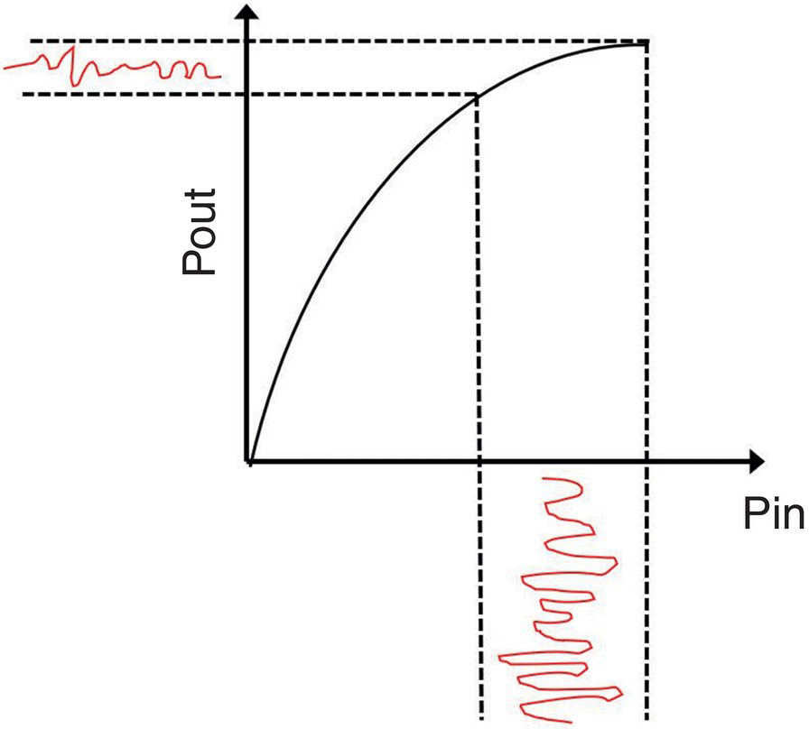
Figure 7.7 The noise suppression of SOA.
Source: [27]/IEEE.
7.3.4 Scalability
The scalability of switches‐based SOAs can be implemented in various schemes. One is the extension of a single stage, another is cascading more stages. Additionally, there are techniques to augment the capability of switching and expanding. For example, the enhanced extinction ratio is offered by the combination of SOA gates and an interferometer, which is a significant index for the scalable network. Moreover, the scaling of switched arrayed waveguide grating is also a feasible method.
Above all, it should first be pointed out: the potential capability for single‐stage 8 × 8 switches at a data capacity of 10 × 10 Gbit/s is predicted to move switch performance to Tbit/s in a relatively simple single‐stage switch fabric with a 1.6 dB power redundancy [28]. Nevertheless, the scalability to even higher levels of connectivity is confined by the incompatibility of existing waveguide crossing and waveguide bend techniques, which contributes to the lack of 8 × 8 switches and the focus on the effort of 1 × 8 monolithic connectivity [29].
Multi‐stage in photonic networks is more complex than the implementation of broadcast‐and‐select architecture. As Figure 7.8 [29] illustrates, it is a switch network proposed to allow the scaling of four outputs per stage using the hybrid Clos/broadcast‐and‐select architecture [30]. The instance is interconnected with three stages to create the larger 16 × 16 network. It is noteworthy that an intermediate loss between each SOA gate in scalable stages limits the connectivity for Tbit/s.
In the experiment of White et al. [30], the power‐ and hardware‐efficient scaling of switched optical networks has been demonstrated with the hybrid architectural approach combining Clos and broadcast‐and‐select routing. The Clos network balances the number of stages and complexity of each switch stage in a suitable case [30]. In the example depicted in Figure 7.9 [30], it is the universal architecture of a three‐stage Clos network. Each twofold scaling in size for the n × n switch is implemented recursively with splitters around 2 × 2 switching elements.

Figure 7.8 The scalable multi‐stage switch architecture with SOAs.
Source: Modified from [29].

Figure 7.9 The architecture of 32 × 32 Clos network.
Source: Modified from [30].
Physical layer scalability is another form of the network. Noteworthily, if we want to create multiport switch from SOA gates, it requires additional interconnecting passive circuit elements. Moreover, the impact of cumulative PDG on the physical layer scalability of space switch can be reduced through proper active region design for an expected SOA gain. However, it can be observed that though the measured noise figure (NF) is slightly smaller at higher gain, the SOA saturates more rapidly, leading to lower space switch scalability. There are many factors influencing the scalability. In our consideration of total power consumption, a larger number of cascaded SOAs at lower gain will not necessarily lead to better performance. While for the same number of ports, the architectures of a space switch determine the number of cascaded SOAs in the routing path and SOAs in the whole system.
Crosstalk will be taken into consideration with the disadvantages on scaling, which are due to non‐ideal filtering and switching. The different order of crosstalk has various contributions on the scalability [31]. The interfering signal if suppressed once is called first‐order crosstalk, of twice is called second‐order crosstalk etc. To maintain the property of system after scaling, the crosstalk must eliminate or suppress in signal switching.
Not merely this, the feasibility demonstration of the scalability in the future is also a noteworthy topic. In the research of Cheng et al. [32], the 64 × 64 SOA‐based optical switch has been theoretically substantiated with an experiment of an 8 × 8 SOA switch. In the simulation of the monolithically‐integrated switch, the results depicted reaching the power penalty minimum as low as 1 dB with such a fully integrated switch.
7.4 Advancements on SOA‐Based Switch
Before the chapter moves on to advanced SOA‐based switches, it is worth concisely indicating the background to retain your perception of the theory of SOA switches. On the configuration of the electrical driving current, it is distinct of the control of the amplifier gain to deploy the on or off state, as shown in Figure 7.10. On the other hand, it is necessary to confirm our reference frequency, shown in Figure 7.11. The conception of switching rise time, which is the important figure of merit in the estimate of the optical space switches, is calculated on the 90–10% of steady‐state output power. With the percentage of the exceeding steady optical signal, the overshoot is defined as the results of calculation. Moreover, the settling time is measured by the difference between the instant in steady level and the pulse start where the steady‐level point is defined as the amplitude no longer higher than 5% of the steady‐state level. Nevertheless, the stabilization point is correlated with the demand of different applications [33].
Afterward, techniques applied on the advancement and aspects are introduced respectively. Above all, the rise time is reduced by the preimpulse step‐injected current (PISIC) in [34], which is based on the control of the injected current for on or off state in the SOA switch. The technique is deployed in the manipulation of carrier density and achieved by the injection of a narrow electric pulse before the valid switching signal impulse, which is implemented on the leading edge. The guarantee of sharp injection of electric carriers allows the increase of the carrier density in the active region of SOAs, which, in consequence, contributes to the faster transition of switching controls. The experimental results show an abrupt reduction of rise time from 2 ns to 200 ps in a bulk material of SOAs.

Figure 7.10 (a) The different electrical switching current drives SOA in on/off state. (b) The consecutive input of modulated optical signal. (c) The gated output signal comes after the pass‐through of SOA biased by the switching current.
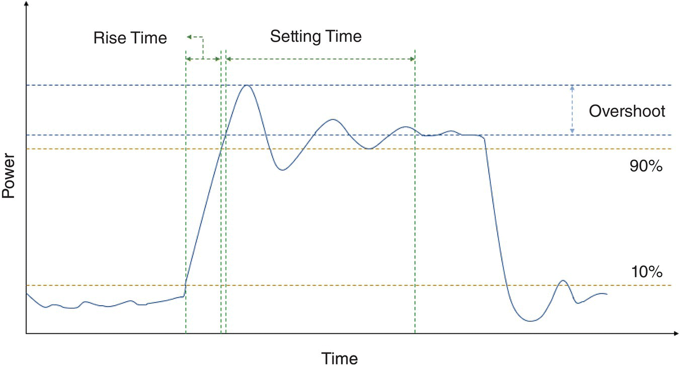
Figure 7.11 The definition of the rise time, settling time, and overshoot.
Nevertheless, to reduce the defect introduced by the PISIC, like the increase of the overshoot and a longer settling time etc., the multi‐impulse step‐injected current (MISIC) is proposed to possibly eliminate the practical impact of the potential results of SOA saturation and longer guard time [35]. The basic operation of the MISIC is the momentary injection of electrical carriers, which will compensate the different impairment in switches of various periods, for example, the undershoot, the gain oscillations, and the relaxation of carriers in SOAs. Altogether, the MISIC employs the extra carriers injected for the increase of the SOA optical gain. However, the stringent impulses synchronized and the evaluations of amplitude oscillation location and duration should be recognized. Moreover, the pulse intensity of every operated point and the higher energy consumption will be also the considerable effects on the implementation. Despite this, the applications of MISIC techniques are possibly waiting below the horizon.
Irrespective of which scheme can eventuate in the design on the basis of electrical switching, the signal is devoted to the compensation for oscillations of the electrical carriers in the SOA active region. Additionally, there are other scenarios like the enhancement of electro‐optical performance through impedance matching and encapsulation optimization. The integration of the devices dramatically scales down while reducing the physical dimensions, improving the energy efficiency, and increasing the optical response bandwidth and stability. For example, the on‐chip SOA‐based optical space switch indicates it is competitive when used in practical applications in datacenters [36, 37].
To demonstrate this scheme, experimental results of the ultra‐wideband in 2020 will be briefly described in this section. Renaudier et al. [38] developed the polarization diversity architecture, leveraging the single polarized SOAs to implement the 100+ Tb/s transmissions with tailor‐made packaged devices. The schematic description of the structure is illustrated in Figure 7.12 [38]. Altogether, the complete integration of electro‐optical parts is the most efficient manner for performance optimization in the application of SOA switches.
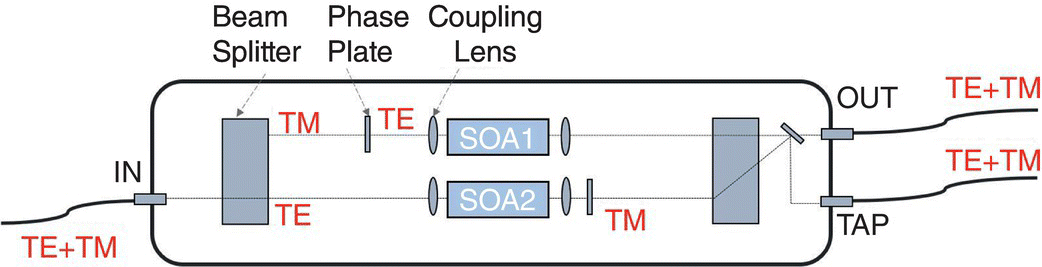
Figure 7.12 Schematic description for the polarization diversity architecture of SOAs.
Source: [38]/IEEE.
7.5 Networks Employing SOA‐Based Switch
Based on the commercial information, theses, and monographs, there are various architectures on the applications of SOAs. The classifications of networks may be based on the application scenario, or the role and position of SOA in the switches to separate them. In this section, the division will be on the basis of application scenarios and optical signal modulations. Moreover, each network deploying SOA‐based switches will be depicted comprehensively.
7.5.1 Metro‐Access Network
The work of Koenig et al. [39] demonstrated the cascade of at least four SOAs that can amplify the advanced‐modulated optical signals in the format of BPSK, QPSK, 8PSK, and 16QAM in the convergence of optical metro networks and access networks. Furthermore, in the work of Calabretta et al. [40], the SOA‐based photonic integrated wavelength division multiplexing (WDM) cross‐connects for optical metro‐access networks realized the switching speed by using an SOA. The main function of SOA enables the selection of any wavelength in the C band and compensates for the losses.
7.5.2 RF Network
Radio over fiber (RoF) is the technique to transmit the radio frequency signals with low dissipation. Shown in the paper of Qian et al. [41], 50 μs switching time has been attained while a proof‐of‐principle 10 × 10 switch is applied in a time‐domain RoF network. It achieved a spurious‐free dynamic range (SFDR) of 96.5dB·Hz2/3 and an error vector magnitude (EVM) of 1.48%, moreover, based on which is scalable and cascaded enabled. Furthermore, the millimeter waves meet the definition of radio simultaneously, 30–300 GHz band. The nonlinear phenomena mentioned before like FWM, SPM, and XGM effects in SOA promote the performance improvement of switches in MMW‐based 5G networks [42].
7.5.3 Silicon Photonic Switching
In the paper of Budd et al. [43], the design of a 4‐channel SOA flip‐chip based on the miscellaneous integration of III–V SOA is implemented in the silicon photonic switches. The photonic carrier with unique SiN waveguide coupling structures were arranged with individual SOAs using the precise flip‐chip bonder (FCB), while a greater than 10 dB net SOA optical gain was recorded. Furthermore, the precise FCB is used in subsequent experiments like the thesis of Matsumoto et al. [44], in which the mode field on both the InP‐SOAs and the Si waveguides was extended by spot‐size converts (SSCs). The gain of the inline optical amplification based on the application of techniques mentioned and inline integration of SOAs with angled waveguides achieved 15 dB. Dramatically, the first demonstration of a lossless Si switch was achieved with the hybrid‐integrated 4‐ch SOA for the 4 × 4 Si switch. Not merely this, the experiment of Konoike et al. [45] is considerable, which fabricated even a four‐stage transmission containing a bit error rate of the transmission signal below 20% forward‐error‐correction confinement with WDM channels.
7.5.4 Data Center Network
With the capacity demand of data center network (DCN), the applications of SOA‐based switches are continuously increasing. In the concise introduction of SOA‐based switches in Cheng et al. [46], the square principle increase of broadcast‐and‐select topology discourages scaling beyond 4 × 4 connectivity on the monolithic integration, which facilitates the application of stages. In the experiment, SOAs as on‐chip gain in photonic WDM switches indicate the fast switching time and high contrast ratio of SOA, designed by Calabretta et al. [47]. Moreover, the SOA gates with nanoseconds switching completely compensated for the loss caused by the photonic integrated wavelength‐selective switch (PIC‐WSS), 8.1 dB, in the paper of Xue [48]. Not merely integrated in the switches, the SOA gain can take a role in the gain of compensating the loss of each buffer module in DCNs, as shown in the experiment of Singh et al. [49].
7.6 Discussion and Future Work
In view of the various researches on SOAs and SOA‐based switches, this section will cover an outline of the matrix switch architectures, a variety of switches of different sorts, and SOAs used in spectrum‐sliced systems. Altogether, the merits and impairments with the future work will be discussed.
The matrix architectures have been indicated by Stabile et al. [50] with space‐division and wavelength division switching, which are classified into four types: (1) multi‐stage, (2) cross‐point, (3) broadcast‐and‐select (B&S) switch, and (4) wavelength‐selective [51]. The basic point‐to‐point structure and point‐to‐multipoint switching architecture are both worth considering. Based on space division, the B&S has the potential to be implemented on the polarization division and mode division.
In the ideal SOA‐based switch, the dynamic procedure is depended on the lifetime of carriers, which in the commercial devices are also influenced by the parasitic elements on switching velocity and overall property. Discussed in the research of Sutili et al. [33], the effects of parasitic elements are the quality of electrical switching pulses, the switch bandwidth reduction, and the dynamic stability, which are identified and quantified based the model presented by them. Moreover, a type of SOA‐based polarization rotation switch on the basis of cross‐polarization modulation in the communication of Raja et al. [52] is proposed and analyzed due to high extinction ratio and low switching energy. In the whole project, the presence or absence of light if polarized with a distinctive state are demonstrated as the feasible operation for the proposed designs. Additionally, on the basis of WSS technique, the optical network for the future adoption is studied by Martín González et al. [53]. The experimental results will be not cited particularly in this chapter, which manifest the performance of the SOA‐based switch depending on the number of SOAs limits.
Furthermore, the thin‐film facet integration is another lively research gate, which has the symmetrical thin‐film resistive, thin‐film microwave coupler etc. Take a brief description of both. The former replaced the typical 47 Ω resistor in the thesis of Figueiredo et al. [54], which achieve the reduction of parasitic elements, 225 ps OFF‐ON time, and 12% overshoot with the fast injection of PISIC, reaching the approximate Gaussian‐response in the electro‐optical spatial switching. Meantime, Sutili et al. [55] led the switch‐time improvements and the reduction of settling time in a near 200 ps spatial switching time. Not merely this, coarse wavelength division multiplexing (CWDM) system with the impetus of capacity and distance extension requires the favorable performance of SOAs on the entire optical bandwidth (from 1260 nm to 1620 nm) meeting the demands. Additionally, the researches on SOA‐based space switch of BER improvement and guard‐time reduction through feed‐forward filtering is also in the scope as Taglietti et al. [56].
Eventually, with the combination of SOAs, it may also be employed in spectrum‐sliced systems in the future, manipulating as both noise suppression and other functions like wavelength conversion in WDM systems. Utilizing the optical nonlinearity properties of a saturated‐SOA, it is a promising approach to reach the intensity noise suppression with the best suited performance as mentioned in the comparison of Jindal et al. [57]. The advantages of SOAs broadens the applications of SOA‐based switches.
Altogether, with the development of hybrid architecture of SOAs and other techniques, the merits of integration, doping, nonlinearity, noise suppression, scalability, simplicity, high efficiency, and relative low cost will consecutively facilitate switching or other applications on the basis of SOAs.
Bibliography
- 1 D. Forsyth and F. Mahad. Semiconductor optical amplifiers: present and future applications. In N. Zulkifli, editor, Recent Developments in Optical Communication and Networking, Penerbit UTM Press, 2020.
- 2 T. Akiyama, M. Sugawara, and Y. Arakawa. Quantum‐dot semiconductor optical amplifiers. Proceedings of the IEEE, 95:1757–1766, 2007.
- 3 A. Assadihaghi, H. Teimoori, and T.J. Hall. 6 – SOA‐based optical switches. In: B. Li, S.J. Chua, editors. Optical Switches. Woodhead Publishing, 2010, 158–180.
- 4 R.C. Figueiredo, E.C. Magalhães, N.S. Ribeiro, C.M. Gallep, and E. Conforti, editors. Equivalent circuit of a semiconductor optical amplifier chip with the bias current influence. In 2011 SBMO/IEEE MTT‐S International Microwave and Optoelectronics Conference (IMOC 2011, 29 Oct – 1 Nov 2011.
- 5 G.T. Kennedy, P.D. Roberts, W. Sibbett, D.A.O. Davies, M.A. Fisher, and M.J. Adams, editors. Intensity dependence of the transparency current in InGaAsP semiconductor optical amplifiers. Summaries of papers presented at the Conference on Lasers and Electro‐Optics, 2–7 June 1996.
- 6 D.V. Taco, L. Daan, and B. Hans, editors. Polarization sensitivity of the amplification in semiconductor optical amplifiers. In Proc. SPIE 2994, Physics and Simulation of Optoelectronic Devices V, 6 June 1997. doi: 10.1117/12.275612.
- 7 D.R. Paschotta. Optical amplifiers based on semiconductor gain media. Encyclopedia of Laser Physics and Technology. www.rp‐photonics.com/semiconductor_optical_amplifiers.html. 2008.
- 8 Z. Zhu, X. Li, and Y. Xi. A polarization insensitive semiconductor optical amplifier. IEEE Photonics Technology Letters, 28(17):1831–1834, 2016.
- 9 T. Kaizu, T. Kakutani, K. Akahane, and T. Kita. Polarization‐insensitive fiber‐to‐fiber gain of semiconductor optical amplifier using closely stacked InAs/GaAs quantum dots. Japanese Journal of Applied Physics, 59(3):032002, 2020.
- 10 M. Yamada, editor. Noise in semiconductor optical amplifiers (SOA). In 2016 IEEE 6th International Conference on Photonics (ICP), 14–16 March 2016.
- 11 Vitextech. OSNR in Fiber Optic Communications. https://vitextech.com/osnr‐meaning/.
- 12 OSNR: What does this mean; Why do we need and How to take care of it? 18 July, 2019. https://mapyourtech.com/entries/general/osnr‐what‐does‐this‐mean‐why‐do‐we‐need‐and‐how‐to‐take‐care‐of‐it‐.
- 13 M. Yamada. Analysis of intensity and frequency noises in semiconductor optical amplifier. IEEE Journal of Quantum Electronics, 48(8):980–990, 2012.
- 14 O. Qasaimeh. Effect of doping on the optical characteristics of quantum‐dot semiconductor optical amplifiers. Journal of Lightwave Technology, 27(12):1978–1784, 2009.
- 15 K. Vahala and C. Zah. Effect of doping on the optical gain and the spontaneous noise enhancement factor in quantum well amplifiers and lasers studied by simple analytical expressions. Applied Physics Letters, 52:1945–1947, 1988.
- 16 V. Cesari, W. Langbein, and P. Borri. The role of p‐doping in the gain dynamics of InAs/GaAs quantum dots at low temperature. Applied Physics Letters, 94:041110, 2009.
- 17 V. Cesari, W. Langbein, P. Borri, M. Rossetti, A. Fiore, S. Mikhrin et al. Ultrafast gain dynamics in 1.3μm InAs/GaAs quantum‐dot optical amplifiers: The effect of p doping. Applied Physics Letters, 90:201103, 2007.
- 18 D. Razmjooei, A. Zarifkar, M.H. Sheikhi, editors. Effect of optical pumping to the wetting layer and excited state on the gain dynamics of QD‐VCSOA: An equivalent circuit approach. In 2017 Iranian Conference on Electrical Engineering (ICEE), 2–4 May 2017.
- 19 G. Talli and M.J. Adams. Gain dynamics of semiconductor optical amplifiers and three‐wavelength devices. IEEE Journal of Quantum Electronics, 39(10):1305–1313, 2003.
- 20 V. Lal, M.L. Masanovic, J.A. Summers, G. Fish, D.J. Blumenthal. Monolithic wavelength converters for high‐speed packet‐switched optical networks. IEEE Journal of Selected Topics in Quantum Electronics, 13(1):49–57, 2007.
- 21 L. Occhi, Y. Ito, H. Kawaguchi, L. Schares, J. Eckner, and G. Guekos. Intraband gain dynamics in bulk semiconductor optical amplifiers: measurements and simulations. IEEE Journal of Quantum Electronics, 38(1):54–60, 2002.
- 22 B.F. Kennedy, P. Landais, and A.L. Bradley, editors. Experimental analysis of polarization dependence of ultrafast gain dynamics in SOAs. In Proceedings of SPIE, 5825, Opto‐Ireland 2005: Optoelectronics, Photonic Devices, and Optical Networks, 2005.
- 23 A. Reale, A.D. Carlo, and P. Lugli. Gain dynamics in traveling‐wave semiconductor optical amplifiers. IEEE Journal of Selected Topics in Quantum Electronics, 7(2):293–299, 2001.
- 24 T.W. Berg, J. Mørk, and J.M. Hvam. Gain dynamics and saturation in semiconductor quantum dot amplifiers. New Journal of Physics, 6:178, 2004.
- 25 K. Kim, J. Urayama, T. Norris, J. Singh, J. Phillips, and P. Bhattacharya. Gain dynamics and ultrafast spectral hole burning in In(Ga)As self‐organized quantum dots. Applied Physics Letters, 81:670–672, 2002.
- 26 T. Yamatoya, F. Koyama, and K. Iga, editors. Noise suppression and intensity modulation using gain‐saturated semiconductor optical amplifier. In Proceedings Optical Amplifiers and Their Applications, 9 July 2000, Québec City: Optical Society of America.
- 27 F. Koyama, and H. Uenohara, editors. Noise suppression and optical ASE modulation in saturated semiconductor optical amplifiers. In Conference Record of the Thirty‐Eighth Asilomar Conference on Signals, Systems and Computers, 7–10 November 2004.
- 28 T. Lin, K.A. Williams, R.V. Penty, I.H. White, M. Glick, and D. McAuley. Performance and scalability of a single‐stage SOA switch for 10×10 Gbs wavelength striped packet routing. IEEE Photonics Technology Letters, 18(5):691–693, 2006.
- 29 R. Stabile and K.A. Williams. Photonic integrated semiconductor optical amplifier switch circuits. In P. Urquhart, editor. Advances in Optical Amplifiers. InTechOpen, 2011.
- 30 I.H. White, E.T. Aw, K.A. Williams, H. Wang, A. Wonfor, R.V. Penty. Scalable optical switches for computing applications. Journal of Optical Networking, 8:215–224, 2009.
- 31 L. Gillner, C.P. Larsen, M. Gustavsson. Scalability of optical multiwavelength switching networks: crosstalk analysis. Journal of Lightwave Technology, 17(1):58–67, 1999.
- 32 Q. Cheng, M. Ding, A. Wonfor, J. Wei, R.V. Penty, and I.H. White, editors. The feasibility of building a 64×64 port count SOA‐based optical switch. 2015 International Conference on Photonics in Switching (PS), 22–25 September 2015.
- 33 T. Sutili, R.C. Figueiredo, B. Taglietti, C.M. Gallep, E. Conforti. Ultrafast electro‐optical switches based on semiconductor optical amplifiers. In: A. Paradisi, R. Carvalho Figueiredo, A. Chiuchiarelli, and E. de Souza Rosa, editors. Optical Communications: Advanced Systems and Devices for Next Generation Networks. Cham, Springer International Publishing, 2019. p. 17–40.
- 34 C.M. Gallep and E. Conforti. Reduction of semiconductor optical amplifier switching times by preimpulse step‐injected current technique. IEEE Photonics Technology Letters, 14(7):902–904, 2002.
- 35 R.C. Figueiredo, N.S. Ribeiro, A.M.O. Ribeiro, C.M. Gallep, and E. Conforti. Hundred‐picoseconds electro‐optical switching with semiconductor optical amplifiers using multi‐impulse step injection current. Journal of Lightwave Technology, 33(1):69–77, 2015.
- 36 A. Wonfor, H. Wang, R. Penty, I. White. Large port count high‐speed optical switch fabric for use within datacenters [Invited]. IEEE/OSA Journal of Optical Communications and Networking, 3(8):A32–A39, 2011.
- 37 R. Stabile, A. Albores‐Mejia, and K.A. Williams. Monolithic active‐passive 16×16 optoelectronic switch. Optics Letters, 37(22):4666–4668, 2012.
- 38 J. Renaudier, A. Arnould, A. Ghazisaeidi, D.L. Gac, P. Brindel, E. Awwad, M. Makhsiyan, K. Mekhazni, F. Blache, A. Boutin, L. Letteron, Y. Frignac, N. Fontaine, D. Neilson, and M. Achouche. Recent advances in 100+nm ultra‐wideband fiber‐optic transmission systems using semiconductor optical amplifiers. Journal of Lightwave Technology, 38(5):1071–1079, 2020.
- 39 S. Koenig, R. Bonk, H. Schmuck, W. Poehlmann, T. Pfeiffer, and C. Koos, et al. Amplification of advanced modulation formats with a semiconductor optical amplifier cascade. Optics Express, 22(15):17854–17871, 2014.
- 40 N. Calabretta, W. Miao, K. Mekonnen, and K. Prifti. SOA based photonic integrated WDM cross‐connects for optical metro‐access networks. Applied Sciences, 7(9):865, 2017.
- 41 Q. Xin, P. Hartmann, L. Sheng, R.V. Penty, and I.H. White, editors. Application of semiconductor optical amplifiers in scalable switched radio‐over‐fiber networks. In 2005 International Topical Meeting on Microwave Photonics, 14 October 2005.
- 42 F. Saadaoui, M. Fathallah, A.M. Ragheb, M.I. Memon, H. Fathallah, S.A. Alshebeili. Optimizing OSSB generation using semiconductor optical amplifier (SOA) for 5G millimeter wave switching. IEEE Access, 5:6715–6723, 2017.
- 43 R.A. Budd, L. Schares, B.G. Lee, F.E. Doany, C. Baks, and D.M. Kuchta, et al., editors. Semiconductor optical amplifier (SOA) packaging for scalable and gain‐integrated silicon photonic switching platforms. In 2015 IEEE 65th Electronic Components and Technology Conference (ECTC), 26–29 May 2015.
- 44 T. Matsumoto, T. Kurahashi, R. Konoike, K. Suzuki, K. Tanizawa, A. Uetake, et al. Hybrid‐Integration of SOA on Silicon Photonics Platform Based on Flip‐Chip Bonding. Journal of Lightwave Technology, 37(2):307–313, 2019.
- 45 R. Konoike, K. Suzuki, T. Inoue, T. Matsumoto, T. Kurahashi, A. Uetake, K. Takabayashi, S. Akiyama, S. Sekiguchi, S. Namiki, H. Kawashima, and K. Ikeda. SOA‐integrated silicon photonics switch and its lossless multistage transmission of high‐capacity WDM signals. Journal of Lightwave Technology, 37(1):123–130, 2019.
- 46 Q. Cheng, S. Rumley, M. Bahadori, and K. Bergman. Photonic switching in high performance datacenters [Invited]. Optics Express, 26(12):16022–16043, 2018.
- 47 N. Calabretta, K. Prifti, N. Tessema, X. Xue, B. Pan, and R. Stabile, editors. Photonic integrated WDM cross‐connects for optical metro and data center networks. ProcSPIE, Metro and Data Center Optical Networks and Short‐Reach Links II, 2019.
- 48 X. Xue, F. Nakamura, K. Prifti, B. Pan, F. Yan, and F. Wang, et al. SDN enabled flexible optical data center network with dynamic bandwidth allocation based on photonic integrated wavelength selective switch. Optics Express, 28(6):8949–8958, 2020.
- 49 P. Singh, J. Rai, and A. Sharma. Analysis of AWG‐based optical data center switches. Journal of Optical Communications, 42, 2019. doi: 10.1515/joc‐2019‐0140.
- 50 R. Stabile, A. Albores‐Mejia, A. Rohit, and K.A. Williams. Integrated optical switch matrices for packet data networks. Microsystems & Nanoengineering, 2(1):15042, 2016.
- 51 R. Soref. Tutorial: Integrated‐photonic switching structures. APL Photonics, 3(2):021101, 2018.
- 52 A. Raja, K. Mukherjee, and J.N. Roy. Design analysis and applications of all‐optical multifunctional logic using a semiconductor optical amplifier‐based polarization rotation switch. Journal of Computational Electronics, 20(1):387–396, 2021.
- 53 L. Martín González, S. Van der Heide, X. Xue, J. Van Weerdenburg, N. Calabretta, and C. Okonkwo, et al. Programmable adaptive BVT for future optical metro networks adopting SOA‐based switching nodes. Photonics, 5(3):24, 2018.
- 54 R.C. Figueiredo, T. Sutili, N.S. Ribeiro, C.M. Gallep, and E. Conforti. Semiconductor optical amplifier space switch with symmetrical thin‐film resistive current injection. Journal of Lightwave Technology, 35(2):280–287, 2017.
- 55 T. Sutili, R. Figueiredo, N. Ribeiro, C.M. Gallep, and E. Conforti. Improvements evaluation of high‐speed electro‐optical integrated thin‐film microwave coupler SOA‐based space switch. Journal of Microwaves, Optoelectronics and Electromagnetic Applications, 17:477–485, 2018.
- 56 B. Taglietti, T. Sutili, R.C. Figueiredo, R. Ferrari, and E. Conforti. Semiconductor optical amplifier space switch BER improvement and guard‐time reduction through feed‐forward filtering. Optics Communications, 426:295–301, 2018.
- 57 J. Jindal, A. Kumar, and R. Kumar. Evaluation and analysis of different spectrum slicing techniques in free space optical systems. In IOP Conference Series: Materials Science and Engineering, 1033:012074, 2021.