
Chapter 2
Antenna Matching
The most important thing one must always remember when designing a matching circuit for antenna is that only inductors or capacitors can be used. In active microwave circuit designs, such as amplifier designs, resistors are frequently used to improve the port matching and circuit stability [1]. But in antenna designs, one should NEVER use resistors or other lossy components. The whole purpose of an antenna in a cellular device is to transmit or receive power, so the efficiency of the antenna is the most critical parameter. Whenever a resistor is added to a matching circuit, the efficiency always drops and that is not our goal. This mistake is repeatedly made by amateur antenna designers, so it is better to set the record straight before we start this chapter.
In this chapter, familiarity with basic electromagnetic concepts, such as characteristic impedance, return loss, reflection coefficient, voltage standing wave ratio (VSWR), and transmission line is assumed. If not, then the following textbooks are recommended before continuing [2–5]. An understanding of the Smith Chart, which is the essential tool used in any antenna matching, is also recommended.
For those who want to have an in-depth report of matching techniques used in microwave circuit matching, the book by Professor Gonzalez, Microwave Transistor Amplifiers: Analysis and Design, [1] is a good reference. A paper by Professor Cripps [6] also provides some good discussions on the matching issue from a different point of view.
Matching is a useful technique in antenna designs. It gives engineers some more design freedom. But one has to remember that matching is not the silver bullet to solve all antenna design problems. Matching circuits are always associated with some degree of loss, which is due to the limited quality factor inherent in all components, no matter whether they are inductors, capacitors, or distributed networks. If an antenna has a reasonable initial resonance, the improvement obtained from the matching circuit will compensate for the loss it introduces. But if the antenna is not well designed, good performance will never be achieved by any matching circuit.
Free software, ZJ_Antenna_Matching, can be found on this book's companion web site. Detailed instructions of how to use this software can be found in the Appendix. The data files of all examples of this chapter can also be found on the companion web site. To really master the matching techniques, it is strongly recommended that these examples are attempted.
The essential aim of matching is to convert the original antenna impedance to a new one, which is as close to the system's characteristic impedance as possible. In the case of the mobile phone, the target impedance is normally 50 Ω. The 50 Ω is not a magic value existing exclusively in the world, there are other standards, for example, 75 Ω and 300 Ω, which are widely used in the broadcasting industry. The 50 Ω is only an industry standard for cellular antenna business. Most radio frequency (RF) equipment used by cellular phone companies and cellular phone antenna vendors use 50 Ω ports as the standard interface. The 50 Ω is chosen as the default characteristic impedance in this book. Nevertheless the matching techniques discussed here can be used in antenna designs of any characteristic impedance.
To measure the effectiveness of a matching circuit, one needs a quantitative value. The voltage reflection coefficient Γ can serve this purpose. The voltage reflection coefficient Γ is the ratio between the reflected wave and the incidence wave. Γ is defined in Equation (2.1).
where ![]() and
and ![]() , both of them are complex values and can be represented by amplitude and phase, are voltages of reflected wave and incident wave respectively. Voltage reflection coefficient Γ is also a complex value. To evaluate the matching of antennas, only the amplitude of Γ, which is denoted as |Γ|, matters.
, both of them are complex values and can be represented by amplitude and phase, are voltages of reflected wave and incident wave respectively. Voltage reflection coefficient Γ is also a complex value. To evaluate the matching of antennas, only the amplitude of Γ, which is denoted as |Γ|, matters. ![]() is the phase angle of Γ. When a signal is fed to a load, in our case the load is an antenna, if the load has the same characteristic impedance as the transmission line, this load is a matched one and only the incidence wave travels from the source to the load on the transmission line, and the minimum reflection coefficient |Γ|, which is 0, is achieved. When the load is open or short circuit, all the incidence wave is reflected back and travels from the load to the source, and the reflection coefficient |Γ| reaches the maximum value 1.
is the phase angle of Γ. When a signal is fed to a load, in our case the load is an antenna, if the load has the same characteristic impedance as the transmission line, this load is a matched one and only the incidence wave travels from the source to the load on the transmission line, and the minimum reflection coefficient |Γ|, which is 0, is achieved. When the load is open or short circuit, all the incidence wave is reflected back and travels from the load to the source, and the reflection coefficient |Γ| reaches the maximum value 1.
Figure 2.1 shows the complex plane of Γ. These are a set of concentric circles; the amplitudes of any Γ located in the same circle are all equal, thus they have the same level of reflection and can achieve the same level of matching. The worst matching happens when Γ falls in the outmost circle, where |Γ| = 1 and it is also the boundary of Γ plane of any passive system. The origin point of the coordinate system represents the best matching, where |Γ| = 0 and there is no reflection at all.
Figure 2.1 Complex plan of Γ

Γ can also be defined as Equation (2.2). The detailed derivation of Equation (2.2) is omitted in this book. For more information on the derivation, refer to the classical textbooks [2–5].
where ![]() is the load impedance and
is the load impedance and ![]() the characteristic impedance of the source.
the characteristic impedance of the source. ![]() is the normalized load impedance and is a complex value, which can be presented as a real part and an imaginary part given in Equation (2.3).
is the normalized load impedance and is a complex value, which can be presented as a real part and an imaginary part given in Equation (2.3).
where ![]() and
and ![]() are normalized load resistance and normalized load reactance respectively.
are normalized load resistance and normalized load reactance respectively.
As shown in Figure 2.1, when the load is a short circuit ![]() , the Γ takes the value of −1, which is the leftmost point on the real axis. When the load is an open circuit
, the Γ takes the value of −1, which is the leftmost point on the real axis. When the load is an open circuit ![]() , the Γ equals +1, which is the rightmost point on the real axis.
, the Γ equals +1, which is the rightmost point on the real axis.
If we keep the ![]() constant and change the
constant and change the ![]() , the complex value Γ, which can be calculated by Equation (2.2), will generate a curve on the complex Γ plane. If a set of
, the complex value Γ, which can be calculated by Equation (2.2), will generate a curve on the complex Γ plane. If a set of ![]() values is used, a family of curves can be generated. Figure 2.2a shows four curves of constant
values is used, a family of curves can be generated. Figure 2.2a shows four curves of constant ![]() , which are
, which are ![]() , 1 and 2 respectively. The
, 1 and 2 respectively. The ![]() curve is superimposed on the |Γ| = 1 circle shown in the Figure 2.1, which represents situations when the load is lossless and formed by only the reactance component.
curve is superimposed on the |Γ| = 1 circle shown in the Figure 2.1, which represents situations when the load is lossless and formed by only the reactance component.
Figure 2.2 Family of curves of constant ![]() and
and ![]()

In Figure 2.2b, as well as the |Γ| = 1 circle, there are seven constant ![]() line/curves, where
line/curves, where ![]() , ±0.5, ±1 and ±2 respectively. When
, ±0.5, ±1 and ±2 respectively. When ![]() ,
, ![]() is always a real value, thus Γ is also a real value, and the corresponding constant
is always a real value, thus Γ is also a real value, and the corresponding constant ![]() trace superimposes on the real axis in the Γ plane.
trace superimposes on the real axis in the Γ plane.
If we overlay both Figure 2.2a and 2.2b, what we get is the famous Smith Chart, which is shown in Figure 2.3. Compared with Figure 2.2, there are many more curves of constant ![]() and
and ![]() in Figure 2.3, which makes the Smith Chart looks much complicated than it really is.
in Figure 2.3, which makes the Smith Chart looks much complicated than it really is.
Figure 2.3 The Smith Chart

The correct name for the Smith Chart shown in Figure 2.3 is the Impedance Smith Chart, which represents curves by fixing either the real or the imaginary part of the normalized load impedance.
To get the admittance Smith Chart, one needs to calculate curves by fixing either the real part ![]() or the imaginary part
or the imaginary part ![]() of the normalized load admittance.
of the normalized load admittance.
(2.4) ![]()
The curves of the admittance Smith Chart can be obtained by simply rotating the Impedance Smith Chart by 180°.
Figure 2.4 shows the superposition of both the impedance and the admittance Smith Chart; we will borrow the name from [1] and refer to it as the ZY Smith Chart. A color version of the ZY Smith Chart can be found on the companion web site. The file is from ZY-01-N and is colored by J. Colvin [7].
Figure 2.4 The normalized impedance and admittance Smith Chart (ZY Smith Chart) (Reproduced from J. Colvin, “Color,” Smith Chart Form ZY-01-N, University of Florida, 1997.)

For any complex load impedance, there is only one unique corresponding position in the Smith Chart. Because both the impedance and the admittance Smith Charts are drawn on the same complex Γ plane, the absolute position of a complex load in the Smith Charts is always the same, no matter whether the load is represented by ![]() or
or ![]() .
.
In some textbooks [3–8], the admittance Smith Chart is identical to the impedance Smith Chart. In that case, whenever a conversion between impedance and admittance is needed, the impedance or admittance point must be rotated by 180° on the Γ plane. That method is technically correct, however, it is too cumbersome for hands-on engineering, therefore it can be omitted.
As a reminder, whenever you see a Smith Chart, always remember it is drawn on a complex Γ plane as shown in Figure 2.1. There is a set of hidden concentrical circles of equal |Γ|. The goal of matching is to move the load impedance toward the center, where |Γ| is 0 and is the perfect matching point.
In most test equipment or simulation software, you can only see the impedance Smith Chart or the admittance Smith Chart one at a time, so it is much more convenient if you can virtually superimpose a complementary Smith Chart in your mind to the one displayed on the screen.
When the Smith Chart was invented in the 1930s, it was a design tool. RF engineers could design a circuit with the Smith Chart and a ruler calculator. Of course there are some hand calculations involved. Some might have done this as homework in universities to practice that skill. The most important part is to decide on the circuit. Calculating the component value by hand is no longer necessary because there is software to help you. There are several commercial software packages available, such as Agilent ADS [9], Microwave Office [10], and so on, which can be used to simulate and optimize a matching network. The companion web site to this book includes matching software, ZJ_Antenna_Matching, which is written by the author and distributed as freeware. For most normal antenna matching tasks, ZJ_Antenna_Matching is good enough. It can read a data file saved as TOUCHSTN or in CITIFILE format. A mini-version of the software, which can be executed on Windows® based network analyzers, is also included on the companion web site. Detailed instructions on how to use this software can be found in the Appendix.
2.2.1 Matching with Lumped Elements
As mentioned at the beginning of this chapter, when designing a matching circuit for antennas, only reactance components can be used. In the lumped-element-only matching method, that means only inductors and capacitors can be used. Thus a matching component can only move the antenna impedance or admittance along the curves of equal ![]() or
or ![]() in the ZY Smith Chart respectively. In such situations, the ZY Smith Chart can be simplified like the one shown in Figure 2.5, which has only two sets of circles instead of four sets of curves in a standard ZY Smith Chart. All circles crossing the leftmost point are fixed
in the ZY Smith Chart respectively. In such situations, the ZY Smith Chart can be simplified like the one shown in Figure 2.5, which has only two sets of circles instead of four sets of curves in a standard ZY Smith Chart. All circles crossing the leftmost point are fixed ![]() curves, and all circles crossing the rightmost point are equal
curves, and all circles crossing the rightmost point are equal ![]() curves.
curves.
Figure 2.5 Simplified ZY Smith Chart for lumped-element-only matching

For any antenna impedance located on the ZY Smith Chart, there are always two circles run through it, as shown in Figure 2.6. The right circle is the constant ![]() circle and the left circle is the constant
circle and the left circle is the constant ![]() circle. Starting from the antenna impedance, which is marked by a cross in Figure 2.6, there are four directions, a, b, c, and d. Each of them represents one kind of circuit topologic:
circle. Starting from the antenna impedance, which is marked by a cross in Figure 2.6, there are four directions, a, b, c, and d. Each of them represents one kind of circuit topologic:
- When a series inductor is connected to the antenna, which is shown as Figure 2.7a, the combination impedance of the antenna and the series inductor at the output will move in direction a.
- A series capacitor, shown as Figure 2.7b, will move the impedance in direction b.
- A shunt inductor, shown as Figure 2.7c, will move the impedance in direction c.
- A shunt capacitor, shown as Figure 2.7d, will move the impedance in direction d.
Figure 2.6 Always two circles running through a given impedance on the Smith Chart

Figure 2.7 Four possible connecting methods of matching components

To design antenna matching network frequently, it is strongly recommended that you MEMORIZE the above four scenarios. The whole practice of matching is using these four components to move antenna impedances around on the Smith Chart. Actually the memorization process should not be difficult. In most cases when doing antenna matching, you only need to remember two rules. The first rule is the upper half plane is inductive and the bottom half plane is capacitive, so whenever the impedance needs to be moved up, an inductor is needed, otherwise use a capacitor. The second rule is the right circle is the shunt circle and the left circle is the series circle, so if the impedance needs to be moved along the left circuit, a shunt component is needed, otherwise use a series component. As an example, assume we want to move the impedance from the cross marker to the “b” direction. Because it is down, a capacitor is required. Because it is on the right circle, a series component is needed. Combining both, a series capacitor is the correct choice.
Note the phrase “in most cases” is used in the last paragraph. That means in some cases, the rules are not applied. There are four triangle markers in Figure 2.6, which mark the maximum and minimum points of both circles. After those extreme points, the moving direction of impedance, which is either up or down, will flip, but the component selection should not be changed. For instance, if we want to move the impedance toward direction “b” as shown in Figure 2.6, it does not matter whether the final position is above or below the original location, a series capacitor should always be used. Two points, where the impedance equals 0 or infinity, are the stopping points of impedance movement. For instance, a series capacitor can move an impedance along direction “b” but can never move it over the Z = ∞ point.
Theoretically, all capacitors and inductors are equal. But in reality, components have different specifications. It is an engineer's responsibility to check whether a component is suitable for the matching purpose. On the data sheet of high frequency capacitors, the quality factor Q. is normally specified. For antenna engineers, a higher Q is better. However, Q is a variable dependent on the measured frequency. The measured Q of a capacitor is lower when measured at higher frequency. Different manufacturers might measure Q at different frequencies, so be careful when evaluating capacitors from different manufacturers. As a rule of thumb, the Q should be at least around 1000@1 MHz. There are quite a few manufacturers in the RF capacitor business; the brands the author has used include the Murata® GQM series [11] and the Johanson Technology® S series [12].
For high frequency inductors, there are some more specification needs to be attended to. They are: the quality factor Q, the DC resistance, and the self-resonance frequency (SRF). The selection of Q is similar to that of a capacitor, the higher the better. However, the relation between the Q of an inductor and the measured frequency is reversed. The higher the measured frequency, the higher the Q is. With regard to the DC resistance, of course, lower is better. The SRF is the resonance frequency of an inductor. Because in reality, there is always parasitic capacitance in any inductor, the inductance and parasitic capacitance can form a shunt resonator. The SRF tells us at which frequency the inductor starts to resonante. After SRF, the inductor will no longer function as an inductor. When selecting an inductor, the SRF needs to be safely higher than the working frequency. The highest grade inductor is the wire coil chip inductor. The SRF of wire coil inductors is at least twice as high as their film counterpart; and their DC resistance is less than half that of film inductors. The brands of coil inductors the author has used include the Murata® LQW series [13] and the Coilcraft® 0402HP series [14]. Coil inductors are the most expensive inductors of all kinds. For antenna applications, whose performance is not that critical, a high Q film inductor can also be used. The author has used the Murata® LQG15H series [13] and the Johanson Technology® L series [15]. Coil inductors are suitable for the surface-mount technology (SMT) process, but it is quite difficult to handle manually, so be prepared.
Always remember to check the antenna response whenever the vendor of a component is changed, or the component is replaced by a different type. Although two components are marked with the same inductance or capacitance value, this does not necessarily mean they are identical. Basically, an efficiency measurement in a 3D chamber is the ultimate evaluation method one can always count on.
2.2.2 Different Ways to Accomplish a Single Band Matching
By combining the series inductor, the series capacitor, the shunt inductor, and the shunt capacitor, any value of the load impedance in the Smith Chart can be matched except those spots located on the |Γ| = 1 circle, where the impedance is purely reactive. The purpose of matching is to convert the real part of the load impedance to the source impedance ![]() , and eliminate the imaginary part. If there is no real part in a load impedance, which is the case of any spot on the |Γ| = 1 circle, there is nothing to be converted from.
, and eliminate the imaginary part. If there is no real part in a load impedance, which is the case of any spot on the |Γ| = 1 circle, there is nothing to be converted from.
Figure 2.8 shows two circles in the Smith Chart. The left circle is ![]() and the right circle is
and the right circle is ![]() . Any impedance falling in these two circles can be matched by a single component. A spot on the left or right circle can be matched by a shunt or a series component respectively. Now, it is obvious that any matching task can be broken down into two steps: first, move the impedance to these two circles, then use one single element to move the impedance to the center of the Smith Chart.
. Any impedance falling in these two circles can be matched by a single component. A spot on the left or right circle can be matched by a shunt or a series component respectively. Now, it is obvious that any matching task can be broken down into two steps: first, move the impedance to these two circles, then use one single element to move the impedance to the center of the Smith Chart.
Figure 2.8 Two circles which can be matched by single components

At any spot inside |Γ| = 1 circle on the Smith Chart, there are up to four ways to achieve matching. For example, if an antenna with impedance ![]() , as shown in Figure 2.8, needs to be matched, four sets of matching circuits, which are illustrated in Figure 2.9, can be used.
, as shown in Figure 2.8, needs to be matched, four sets of matching circuits, which are illustrated in Figure 2.9, can be used.
Figure 2.9 Four matching options of single load impedance

- A shunt inductor cascade by a series inductor, as shown in circuit (a) in Figure 2.9a.
- A shunt inductor cascade by a series capacitor, as shown in circuit (b) in Figure 2.9a. Compared to circuit (a), both circuits start with the shunt inductor and move the antenna load toward the r = 1 circle, but the value of the shunt inductor used by circuit (a) and (b) is different. The circuit (a) moves the impedance to hit the bottom part of the r = 1 circle. The inductor of circuit (b) has a smaller value than circuit (a), thus moving the impedance further up, bypassing the spot circuit (a) and hitting the top part of r = 1 circle. When used as a shunt component, an inductor with a smaller value has a larger admittance, and thus moves the load further. On the other hand, a capacitor with a smaller value moves the load less.
- A series inductor cascade by a shunt inductor, as shown in circuit (c) in Figure 2.9b.
- A series inductor cascade by a shunt capacitor, as shown in circuit (d) in Figure 2.9b. Similar to the cases shown in Figure 2.9a, two inductors with different values are used to move the load to two different spots on the g = 1 circle. When used as series component, an inductor with a larger value has a larger impedance, and thus moves the load further. On the other hand, a capacitor with a larger value moves the load less.
The four possible matching schemes give an engineer quite some leeway in actual designs. When the metal surface of an antenna element is exposed to the outside environment, the ESD (Electro-Static Discharge) is a potential hazard to the internal circuit. In this kind of circumstance, both matching circuits (a) and (b) can be used to eliminate the danger, because there is a shunt inductor which electrically shorts the antenna element to the ground from the DC point of view. As a reminder, the effectiveness of using an inductor as the grounding depends on the inductance value. If the inductance is too large, say, above 10 nH, the inductor itself is not enough to take care of the ESD issue, thus only circuit (a), which has a series capacitor functioning as a DC blocker to provide the extra measure, is a feasible solution.
To provide a more intuitive feeling for this event, the component values of circuits shown in Figure 2.9 are illustrated in Figure 2.10. The normalized load impedance is chosen as 0.2-j0.64 [Simulation file: Chap2_Fig.10.s1p], and the working frequency is chosen as 1.0 GHz. When using the ZJ_Antenna_Matching as practice in this example, the highlight feature should be used. The impedance in this example is a point impedance. Without the highlight, the impedance dot is too small to be easily distinguished.
Figure 2.10 Component values of the four circuits used in Figure 2.9

Figure 2.11 illustrates the actual layout of Figure 2.10a on a printed circuit board (PCB). The PCB is a double-sided board. On the back of the PCB there is a whole piece of copper layer functioning as the ground. The signal trace and components are placed on the front of the PCB. The output of the matching circuit is a 50 Ω transmission line. When doing a return loss test, this 50 Ω transmission line can be connected to a network analyzer by a coaxial cable. The pad on the top-right corner is the launch point of the antenna. The component on the left side of the antenna pad is the shunt inductor L1. A shunt component is always bridged between a transmission line and the ground. The component on the bottom-right side of L1 is the series inductor L2. A series component is always inserted in the transmission line. When laying out a series component, the transmission line is broken into two segments by inserting a gap and then the series component is used to bridge the gap.
Figure 2.11 Layout of Figure 2.10a on a printed circuit board

When the load impedance is inside either circles r = 1 or g = 1, as shown in Figure 2.12a or Figure 2.12b, the possible options of matching circuits will drop from four to two. Let's use Figure 2.12a as an example. Because the load is inside the g = 1 circle, there is no component that can move the load impedance to the r = 1 circle. Two possible matching circuits, a series inductor cascade by a shunt capacitor or a series capacitor cascade by a shunt inductor, are shown in Figure 2.12a.
Figure 2.12 Two matching options of single load impedance

For the load impedance shown in Figure 2.12b, these two matching circuits are a shunt capacitor cascade by a series inductor or a shunt inductor cascade by a series capacitor.
2.2.3 Matching with Both Transmission Line and Lumped Elements
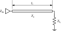
Besides using lumped elements, transmission lines can also move the load impedance around on the Smith Chart. As shown in Figure 2.13, an impedance ![]() is connected by a transmission line with a characteristic impedance of
is connected by a transmission line with a characteristic impedance of ![]() and a length of
and a length of ![]() .
.
Figure 2.13 Load impedance connected by a segment of transmission line
The output impedance ![]() can be expressed by Equation (2.5) [1–5, 8].
can be expressed by Equation (2.5) [1–5, 8].
Here ![]() is a guided wavelength in the transmission line. In Equation (2.5), when
is a guided wavelength in the transmission line. In Equation (2.5), when ![]() , the
, the ![]() , which means the moving path of a transmission line always starts from the
, which means the moving path of a transmission line always starts from the ![]() on the Smith Chart. When
on the Smith Chart. When ![]() , we get
, we get ![]() again, which means the output impedance moves back to the original position when the length of transmission line is half the guided wavelength.
again, which means the output impedance moves back to the original position when the length of transmission line is half the guided wavelength.
Figure 2.14 shows the moving paths of three transmission lines with different ![]() . In this example, the load impedance is
. In this example, the load impedance is ![]() , which is the lower crossing point of all three circles on the Smith Chart. The leftmost circle is the moving path of a transmission line with normalized impedance
, which is the lower crossing point of all three circles on the Smith Chart. The leftmost circle is the moving path of a transmission line with normalized impedance ![]() . The circle in the center corresponds to a transmission line of
. The circle in the center corresponds to a transmission line of ![]() , and the rightmost circle corresponds to
, and the rightmost circle corresponds to ![]() . It can be seen, by increasing the characteristic impedance of the transmission line, that the circle of the moving path shifts from left to right on the Smith Chart. The center of the
. It can be seen, by increasing the characteristic impedance of the transmission line, that the circle of the moving path shifts from left to right on the Smith Chart. The center of the ![]() circle always is superposed on the center of the Smith Chart.
circle always is superposed on the center of the Smith Chart.
Figure 2.14 The impedance's moving path on the transmission lines

A transmission line always moves the load impedance in a clockwise direction on a circle. Thus, to move the impedance to a nearby position on the circle in the anti-clockwise direction, nearly half a wavelength transmission line has to be used.
For any antenna impedance inside or on the r = 1 or g = 1 circles, a perfect matching can be achieved by a single segment of transmission line. For any impedance outside those two circles, it is impossible to obtain a perfect match in this way. However, a match can be achieved by a combination of transmission lines or a combination of transmission line and lumped elements. This book only discusses the latter option. More information on matching with only transmission lines can be found in references [3, 4, 8].
As an example, an impedance ![]() , as shown in Figure 2.15a, needs to be matched. The working frequency is 1 GHz. The design procedure can be divided into two steps. First, move the
, as shown in Figure 2.15a, needs to be matched. The working frequency is 1 GHz. The design procedure can be divided into two steps. First, move the ![]() in a clockwise direction to location a' on the g = 1 circle by a segment of transmission line. Then use a shunt capacitor to move the impedance along the g = 1 circle to the origin of the Smith Chart. The corresponding matching circuit diagram is shown in Figure 2.15 b. To match an impedance of 0.3 + j0.3, a 10 mm-long 50 Ω transmission line and a 2.5 pF shunt capacitor are needed. As demonstrated in Figure 2.14, to move the impedance in the clockwise direction, the characteristic impedance of the transmission line does not have to be 50 Ω. Any transmission line will do. However, the value of the capacitor must be changed accordingly.
in a clockwise direction to location a' on the g = 1 circle by a segment of transmission line. Then use a shunt capacitor to move the impedance along the g = 1 circle to the origin of the Smith Chart. The corresponding matching circuit diagram is shown in Figure 2.15 b. To match an impedance of 0.3 + j0.3, a 10 mm-long 50 Ω transmission line and a 2.5 pF shunt capacitor are needed. As demonstrated in Figure 2.14, to move the impedance in the clockwise direction, the characteristic impedance of the transmission line does not have to be 50 Ω. Any transmission line will do. However, the value of the capacitor must be changed accordingly.
Figure 2.15 Matching with both transmission line and lumped element

Similarly, impedances (b), (c), and (d), shown in Figure 2.16a, can also be matched by a transmission line and a lumped element. The corresponding matching circuits of different loads are shown in Figures 2.16b–d. In the case of load (b), the lumped matching element is a series capacitor. For the case of loads (c) and (d), the lumped matching elements are a series inductor and a shunt inductor respectively.
Figure 2.16 Matching circuits of load impedance b, c, and d (1 GHz)

In fact, impedances (a), (b), (c), and (d), shown in Figures 2.15 and 2.16, can also be matched by the lumped element only matching techniques. Depending on the location of the load impedance on the Smith Chart, the transmission line can be replaced by different lumped elements. For the impedances (a) and (d), the transmission line can be replaced by a series inductor. In the case of the impedances (b) and (c), the replacing lumped element is a shunt capacitor.
Although the transmission line can move any load impedance to the r = 1 circle or g = 1 circle, thus, in theory, the matching technique introduced in this section can be used in all situations. In practice, the transmission line only is used in circumstances when the load impedance is close to the r = 1 or g = 1 circle and is on the anti-clockwise side of either circle. The reason is that the transmission line does not accommodate the lumped element, it occupies the PCB space. The further it needs to move a load impedance, the longer the transmission line is, thus the larger PCB area it occupies. In addition, the PCB also has inherent loss; a long transmission line degrades the efficiency of an antenna even though it matches the antenna impedance.
2.2.4 Bandwidth Consideration
In the discussion above, the antenna impedance is treated as a constant. However, in reality, the antenna impedance varies with frequency. It is always a curve on the Smith Chart. Any matching network can only move a limited portion of the impedance curve to the target matching circle on the Smith Chart, which means there is a bandwidth limit for any matching network. When using the matching techniques described above, the achievable bandwidth does not vary too much, no matter which match circuit is used.
In this section, the emphasis is on various techniques which can expand the antenna bandwidth. Using matching to increase the bandwidth can also be treated as a wide band impedance matching problem. Professor Cripps' article [6] is a very good reference on this topic, and it provides a short list of references to investigate this area further. This section focuses on techniques frequently used in antenna matching designs. Those complex techniques and theoretical analyses are outside the scope of this book. In this section, three examples are discussed. The Example 2.1 antenna has a decent return loss without any matching, so the matching circuit is used to mainly widen the bandwidth. Example 2.2 describes how to achieve both impedance matching and bandwidth enhancement by an π-shape matching circuit. The techniques discussed in Section 2.2.2 are also applied to Example 2.2 to provide a straightforward comparison between different matching methods. Example 2.3 briefly demonstrates how to use the T-shape network to achieve matching and bandwidth improvement.
Example 2.1
Let's look at Example 2.1 [Simulation file: Chap2_example1.s1p]. Assuming there is an antenna with decent self-resonance at 1.35 GHz, as shown in Figure 2.17, Figure 2.17a and Figure 2.17b are the reflection coefficient and the impedance curve of the antenna. The antenna impedance at a frequency lower or higher than 1.35 GHz is capacitive or inductive respectively. The solid line circle in Figure 2.17b is the S11 equal to −15 dB circle. To increase the bandwidth, an intuitive thought is to squeeze more impedance curve into the −15 dB circle.
To squeeze the impedance line of higher frequency, a shunt capacitor is needed. However, to squeeze the impedance line at a lower frequency band, a shunt inductor is needed. It seems a contradictory requirement at first glance. Fortunately, a shunt LC resonator has the preferred characteristic. The resonant frequency of a circuit shown in Figure 2.18a is decided by:
Figure 2.17 Antenna example – bandwidth widened

Figure 2.18 Shunt LC resonator as a matching circuit

where L and C are the inductance and the capacitance respectively. By selecting the appropriate L and C, the resonant frequency can be allocated to 1.35 GHz; this provides the required reactance condition to bend the impedance curve into the −15 dB circle. From Equation (2.6), it is clear that there are infinite combinations of L and C which generate the same resonant frequency. But different L and C combinations bend the impedance curve differently, thus the achieved bandwidth is also different. Figures 2.18b and c show simulated results. In both figures, the solid line is the result of L = 4.8 nH and C = 2.9 pF. The dashed line is the result of L = 6.7 nH and C = 2.1 pF. In this example, the circuit of L = 4.8 nH and C = 2.9 pF gives the widest −15 dB bandwidth.
Example 2.2
Figure 2.19 shows the original S11 and complex impedance on the Smith Chart of Example 2.2 [Simulation file: Chap2_example2.s1p]. The best matching is achieved at 1.35 GHz with a S11 of merely −3.5 dB. The specification of return loss used in the example is −10 dB.
For the purposes of comparison, a basic two-element circuit shown in Figure 2.20a is used to achieve the required matching. Looking from the antenna side, the matching circuit is composed of a 2.1 nH series inductor and a 3.7 pF shunt capacitor. As shown in Figure 2.20c, the 2.1 nH inductor moves the impedance at 1.4 GHz along the clockwise direction to hit the g = 1 circle, then the 3.7 pF capacitor moves the impedance along the g = 1 circle to the matching area. Figure 2.20b is the S11 of the matched antenna. The S11 is better than −16 dB at 1.4 GHz, and the −10 dB bandwidth is 70 MHz.
Figure 2.21a shows a π-shape matching network, which achieves both antenna matching and bandwidth expanding. Looking from the antenna side, the matching network is composed of a 15.3 pF shunt capacitor, a 2.1 nH series inductor, and an 8.9 pF shunt capacitor. From Figure 2.21b, it is clear that the −10 dB bandwidth is 180 MHz, which is more than twice as much as the bandwidth achieved by the matching network shown in Figure 2.20. Comparing Figure 2.20c and Figure 2.21c, it is clear that the impedance curve of the two-element matching simply passes by the origin point of Smith Chart, meanwhile the impedance curve of the π-shape matching circles around origin point, which generates the double resonance phenomena on S11 results shown in Figure 2.21b.
The working principle of π-shape matching can be explained by mathematically deduced formulas, which can be found in various books on filter designs. A more intuitive explanation is given in this book. There are three components in the π-shape matching circuit. Each component serves a distinct purpose. To separate the con-tribution of each matching component, components are added to the circuit one by one. Figure 2.22a shows the effect of the first capacitor if looking from the antenna side. The dashed line curve in Figure 2.22a is the original impedance curve without matching. The solid line curve is the impedance with the first capacitor added. Compared with the shunt capacitor used in Figure 2.20, which is 3.7 pF, the capacitance of the first capacitor is much larger, up to 15.3 pF. For a shunt capacitor, a higher value means it moves the impedance further on the Smith Chart. The other property of a shunt capacitor is that it moves the impedance at the higher frequency band faster than that at the lower band. In this example, the impedances at lower and the higher frequencies are moved around 110° and 200° respectively. It is the first shunt capacitor which tightens up the impedance curve to generate a loop.
Figure 2.22b shows the impedance curve when both C1 and L1 are added. The effect of L1 is quite clear, which is moving the impedance along in a clockwise direction to hit the g = 1 circle. A series inductor has a similar frequency dependence property as a shunt capacitor, thus besides the impact of moving impedance, it also makes the loop tighter. Figure 2.22c shows the effect of the third matching component, the 8.9 pF shunt capacitor. It moves the impedance on the g = 1 circle to the center of the Smith Chart. Compared with the basic matching circuit shown in Figure 2.20, the C2 capacitor needs to move the impedance further, thus its capacitance is also much larger.
Besides using a shunt capacitor as the first component to generate the required loop as shown in Figure 2.22a, a shunt inductor also has a similar effect. Figure 2.23a shows another version of the π-shape matching circuit. Starting from the antenna side, the first matching component is a 0.73 nH shunt inductor, followed by a 6.9 pF series capacitor and a 1.35 nH shunt inductor. The 0.73 nH shunt inductor L1 generates the required loop. The capacitor C2 moves the impedance along the anti-clockwise direction to hit the bottom part of g = 1 circle. The L2 moves the impedance on the g = 1 circle to the center of the Smith Chart. When an inductor is used as a shunt component, the smaller the value, the larger the impact. Compared with inductor values used in a basic two-element matching circuit, both inductors shown in Figure 2.23 have quite small values. That means both of them move the impedance further. The −10 dB bandwidth obtained by Figure 2.23 is 180 MHz, which is same as the one achieved by the matching circuit shown Figure 2.21.
Figure 2.19 Original antenna impedance before matching

Figure 2.20 Two-element matching circuit
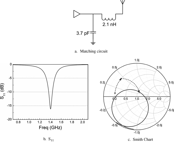
Figure 2.21 π-shape matching circuit
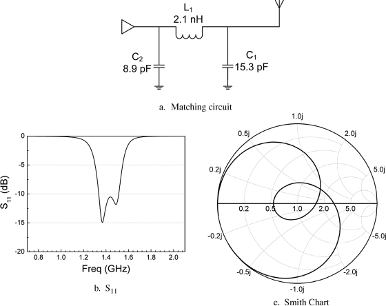
Figure 2.22 Contribution of each component

Figure 2.23 Another version of the π-shape matching circuit

Figure 2.24 T-shape matching circuit

Example 2.3
For an antenna with an impedance similar to the one shown in Figure 2.19, only a π-shape matching circuit can serve the purpose of expanding the antenna bandwidth. In Example 2.3, the original antenna impedance is shown in Figure 2.24a [Simulation file: Chap2_example3.s1p]. For this type of antenna impedance, a T-shape matching network shown in Figure 2.24b is the appropriate choice. Starting from the antenna side, the first matching component is a 0.33 pF series capacitor, followed by a 15.8 nH shunt inductor and a 0.56 pF series capacitor. A detailed explanation is omitted here, because the design consideration is similar to those demonstrated in Figures 2.21 and 2.23.
When compared with a two-element matching, a π-shape matching or a T-shape matching can significantly improve the antenna bandwidth, however, there is a price to pay. Because the components used in π-shape matching or a T-shape matching must move the impedance further, they are more sensitive to manufacturing variation. Figure 2.25 is the yield analysis results of circuits shown in Figures 2.20 and 2.21 respectively. The tolerance of all components used in the simulation is assumed to be ±5% uniformly distributed. Figure 2.25a is the yield results of a two-element matching. The results of 200 simulations are superimposed on Figure 2.25 by light gray lines. The black line is the optimal response when there is no tolerance. The designed −10 bandwidth of the two-element matching is 70 MHz. If selecting a 50 MHz bandwidth as the specification, the yield rate is 96%. On the contrary, although the design bandwidth of the π-shape matching is 180 MHz, the yield is only 81%, even using the same 50 MHz bandwidth as the specification. The yield analysis of the π-shape matching is carried out again using a 100 MHz bandwidth as the specification. As expected, the yield drops to 74% this time.
Figure 2.25 Tolerance analysis (5% of component value)

It is now clear that the bandwidth expanding techniques are not a free lunch. They have some inherent risks. If using a complex matching circuit, select components with tighter tolerance, manufacture antenna more cautiously, and always remember to do a thorough yield analysis.
The bandwidth of an antenna is constrained by the physical volume it occupies. If an antenna has enough volume, it is not difficult to design an antenna to cover all the required bands, even without the help of any matching network. But if the antenna size is limited, the matching circuit can give the designer much more freedom. When designing a dual band antenna in a limited space, it is normal practice to optimize one band, then use the matching circuit to take care of the other band. Some devices have more than one position, such as the flip open and the flip close positions on a clam shell phone, the dual band matching techniques are also very handy when a balanced performance needs to be achieved in all bands and all positions.
As shown in Figure 2.26, the building blocks of dual band matching, which are the series capacitors, the shunt inductors, the series inductors, and the shunt capacitors, are the same as those used in the single band matching. But the components that can be used at each band are limited to two. Using the series inductor as an example, at very low frequencies the complex impedance of a series inductor is close to 0, thus it has no effect on a circuit. At very high frequencies, a series inductor is equivalent to an open circuit, which totally breaks the circuit. As a rule of thumb, when selecting a matching component, the component should have more impact in the target band and less effect in the other band. Thus a series inductor should only be used to match the higher band. Similarly, shunt capacitors can also be used in the higher band matching. When the band that needs to be matched is the lower band, only the shunt inductor and the series capacitor can be used.
Figure 2.26 Matching components for low band and high band respectively

As an example, a dual band matching scenario is shown in Figure 2.27a. The impedance at low band and high band are marked as L and H respectively on the Smith Chart. In an ideal world, where components used for high band only impact the high band, the circuit shown in Figure 2.27b is one of many possible choices to match both bands. The shunt capacitor C1 moves the high band impedance to the bottom part of r = 1 circle; then the series inductor L1 moves it to the center of the Smith Chart. Similarly, the shunt inductor L2 moves the lower band impedance to the top part of r = 1 circle; then the series capacitor C2 moves it to the center.
Figure 2.27 Dual band matching Example 2.1

Figure 2.28 shows an example where the load impedances are the same as shown in Figure 2.27a, however, the corresponding band of each load impedance is reversed. The impedance on the top half is now the low band one. The matching circuit is shown in Figure 2.28b. It is still assumed that each component only impacts its corresponding low or high bands. In an ideal world, if the relative sequence between L1/C1 and C2/L2 can be kept, any variants in Figure 2.28b should have the same frequency response. Figures 2.28c and d are two equivalent variants under the ideal assumption.
Figure 2.28 Dual band matching Example 2.2

In reality, a component cannot exclusively influence one specific band. It always influences both bands simultaneously. Figure 2.28 only shows a few variants; there are tens of possible permutations and combinations. When optimizing the component sequence of a matching circuit, both experience and trial and error play a role. The achievable bandwidth and value of matching component depend on the circuit layout. To demonstrate the influence of selection of matching circuit, an antenna [Simulation file: Chap2_Fig.29.s1p] with S11 and impedance curves shown in Figures 2.29a and b is used. The optimization goal of matching is to achieve a S11 better than −20 dB at both 0.98∼1.02 GHz and 1.67∼1.73 GHz.
Figure 2.29 Antenna Example 2.3

Figure 2.30a shows a variant of matching circuits, which matches the high band first. In this example, when using the shunt capacitor and the series inductor to match the high band impedance, these components also favorably shift the low band impedance; thus, only a shunt inductor is needed for the low band. In the design process, it is an engineer's responsibility to decide on the circuit layout; the optimizing work can be “subcontracted” to any circuit simulation software. Figure 2.30b is a matching circuit which takes care of the low band first. Similarly, the shunt inductor and the series capacitor have a positive impact on the high band impedance; thus, only a shunt capacitor is needed for the high band. Comparing Figures 2.30a and b, these two circuits have different component values and even different inductor/capacitor counts. But both circuits achieve a similar bandwidth. Figures 2.30c and d are final impedance curves of circuits (a) and (b) respectively. The simulated S11 of circuits (a) and (b) is shown in Figure 2.30g as the solid line and dotted line respectively.
Figure 2.30 Selection of matching circuits

Figure 2.30e is a demonstration of how a component sequence can change the achievable bandwidth. By keeping the component sequence of the low band matching block of Figure 2.30b, and only flipping the matching blocks of low and high band, the achievable bandwidth is shrunk.
It has been mentioned that the component sequence in each band cannot be flipped. Figure 2.30f shows an example which has flipped the component sequence of low band. The simulated result, which is far from the optimization goal, is also shown in Figure 2.30g. The result intuitively demonstrates that the component sequence in each band is critical.
So far, all the techniques discussed belong to the category of fixed matching, which means whenever an antenna design is finished, the antenna matching network is fixed and the antenna bandwidth is also fixed. It is well known that the bandwidth of an antenna is constrained by the physical volume it occupies. The static bandwidth of an antenna has a physical limit, which cannot be passed even with the help of matching networks. Note the word “static” in the last sentence. Actually that is the key to breaking the physical limit of antenna bandwidth. Based on the discussion above, it is clear that an antenna can be matched to a wide range of frequency bands by using different matching components and circuit topology. The function of a reconfigurable circuit is to provide various matching statuses based on the control signal, thus achieving good matching in a much wider frequency range.
Although the total working bandwidth of an antenna with reconfigurable matching can surpass the bandwidth limit of the antenna with fixed matching, it does not actually break the physical law. At any given time, the static bandwidth of the antenna is at best equal to the bandwidth achievable by a fixed matching. The total bandwidth of a reconfigurable matching antenna is defined as the summary of all static bandwidths at different status.
The reconfigurable matching is suitable for a system which needs to cover a wide frequency band, but at any given time the system only uses a small portion of that frequency band. For example, the frequency band allocated to the Integrated Services Digital Broadcasting-Terrestrial (ISDB-T) system is 470–770 MHz, but each ISDB-T channel is 6 MHz wide. The reconfigurable solution is a perfect fit in such a system. On the other hand, if a system, such as a device based on the ultra-wideband (UWB) standard, requires a working bandwidth that exceeds the static bandwidth that an antenna can provides, a reconfigurable solution cannot really help.
Another issue that needs to be mentioned is the efficiency degradation due to the loss of reconfigurable circuits. All passive matching components, such as inductors and capacitors, have inherent losses. Similarly, all active components used in reconfigurable circuits, such as a varactor, the pin diodes, the Field-Effect Transistors (FET) switches, or Microelectromechanical systems (MEMS) switches, also have losses. The loss from those switchable devices is accumulated with the existing loss introduced by the passive components, thus decreasing the overall antenna efficiency. If comparing at the same frequency point, the efficiency of an antenna using reconfigurable matching is always less than its counterpart with fixed matching. The reconfigurable matching does provide some performance at the peak of the efficiency curve of an antenna; in exchange, it obtains overall better efficiency in a much wider frequency range.
2.4.1 Reconfigurable Matching – Varactor-Based
The varactor is a diode, when reverse biased, whose capacitance is sensitive to the applied voltage. The higher the reverse bias voltage is on a varactor, the lower capacitance it has. Due to this unique character, a varactor is widely used in electrical tuning devices, such as a voltage controlled oscillator (VCO). In a VCO, the varactor is a part of a resonator which decides the resonant frequency. By adjusting the bias voltage, the capacitance changes, thus causing the change of the working frequency.
As an example, a varactor-based reconfigurable matching is designed for ISDB-T service. The ISDB-T operates at the frequency range of 470–770 MHz, which covers a relative bandwidth of 48.4%. The typical dimensions of a mobile device are quite small in comparison to a quarter of wavelength at 470 MHz, so designing a passive internal ISDB-T antenna to cover the whole band and provide good performance is always a challenge. With the help of reconfigurable matching, a better than −10 dB measured S11 across the 470–770 MHz bandwidth can be achieved.
Without loss of the generality, a meander line antenna is used as the design example. The detailed procedure of how to design a meander line antenna will be discussed in Chapter 3. For now, we only need to use the impedance curve of the meander line antenna. In fact, the antenna element can be replaced by an antenna of any form factor, as long as its impedance has a similar frequency response.
Figure 2.31 shows the impedance curve of the original antenna on the Smith Chart. Three markers on the curve, #1, #2, and #3 denote the highest, median, and lowest working frequency, respectively. There are two considerations in designing a varactor-based antenna matching network. First, the capacitance ratio between the maximum and minimum capacitance which a varactor needs to provide must fall within a reasonable range. Second, the topology of the matching circuit should not be overly complex.
Figure 2.31 Impedance curve of the original antenna

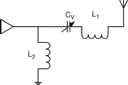
For the impedance curve shown in Figure 2.31a, range of impedance can be matched if a matching network is as shown in Figure 2.32. In this configuration, the antenna is connected by a series varactor Cv, and then followed by a shunt inductor L. The shunt inductor can move any impedance inside the solid line circle area toward the matching point, where the origin of the Smith Chart is. The series varactor can move the other impedance between markers 1 and 2 into the solid line circle. Through the combined effects of the series varactor and shunt inductor, all impedance between markers 1 and 2 can be matched.
Figure 2.32 Matching circuit of the original antenna

Parametric studies and optimizations lead to the conclusion that a meander line antenna element and a varactor with a capacitance ratio of 27.9 (25.1 pF/0.9 pF) are required to achieve the 470–770 MHz bandwidth. To decrease the capacitance ratio required by the varactor, a series inductor L1 is added to the matching network. The final matching circuit layout is shown in Figure 2.33.
Figure 2.33 Diagram of matching circuit
To explain the function of L1, let's reinvestigate the impedance curve shown in Figure 2.31. Besides the impedances between markers 1 and 2 which have been properly matched by a circuit with a series varactor and a shunt inductor, the impedances between markers 2 and 3 also have reasonable return loss and its reactance varies smoothly when the frequency changes. However, this segment of impedance is beyond the reachable tuning range of a matching circuit composed only of a series varactor and a shunt inductor. With the addition of a series inductor, this segment of the impedance line is moved from the bottom to the top of the solid line circle, and thus into the tunable range of the matching circuit. Simulations indicate that the addition of the extra series inductor reduces the required capacitance ratio from 27.9 to 8.2 (7.7 pF/0.94 pF).
To verify the concept of the varactor tuning matching network, a prototype is fabricated and measured. The specific antenna dimensions can be found in Figure 2.34. The antenna element is made of a flat metallic meander line. The element is folded and attached to the outer side of a foam support, whose dimensions are 80∗10∗10 mm3. The antenna is installed on a single-sided FR4 board. The size of the board is 140∗80 mm2, with a thickness of 1.6 mm. The impedance of the antenna without matching has been shown in Figure 2.31.
Figure 2.34 Geometry of meander line antenna: (a) Antenna element (b) Front view (c) Side view (Reprinted from Y. Li, Z. Zhang, W. Chen, Z. Feng and M. Iskander, “A compact DVB-H antenna with varactor-tuned matching circuit,” Microwave and Optical Technology Letters, 52, no. 8, 1786–1789, © 2010, with the permission of John Wiley & Sons, Inc.)

The matching circuit is fabricated on a 10∗10 mm2 double-sided FR4 board shown in Figure 2.35. Most of the components labeled in Figure 2.35 correspond to Figure 2.33, with the exception of Rb and Cp, which are a bias resistor and bypass capacitor supplying bias voltage to the varactor. The varactor used in the experiment is a Skyworks SMV1247-079. The series inductor L1 and shunt inductor L2 used in the experiment are 15 nH and 22 nH, respectively. The back of the matching circuit, a solid piece of copper, which also functions as the ground, is soldered to the big board. Voltage is supplied by three AA batteries. A variable resistor is used to adjust the bias voltage.
Figure 2.35 Layout of matching circuit (Reprinted from Y. Li, Z. Zhang, W. Chen, Z. Feng and M. Iskander, “A compact DVB-H antenna with varactor-tuned matching circuit,” Microwave and Optical Technology Letters, 52, no. 8, 1786–1789, © 2010, with the permission of John Wiley & Sons, Inc.)

Figure 2.36 shows the measured S11 of the antenna with the varactor bias voltage changed from 0 to 3.92 V. Clearly, the operating frequency can be continuously tuned and cover the whole ISDB-T band with S11 better than −10 dB. Based on the specification sheet, the capacitance values are 8.86 pF and 0.78 pF at 0 and 3.92 V bias, respectively. This represents a capacitance ratio of 11.3 rather than the 8.2 obtained in the simulation. It is believed that this discrepancy results from the imperfection of the varactor and parasitic reactance from lumped inductors and circuit board.
Figure 2.36 Measured S11 (Reprinted from Y. Li, Z. Zhang, W. Chen, Z. Feng and M. Iskander, “A compact DVB-H antenna with varactor-tuned matching circuit,” Microwave and Optical Technology Letters, 52, no. 8, 1786–1789, © 2010, with the permission of John Wiley & Sons, Inc.)

Because the capacitance of a varactor is sensitive to the bias voltage, a varactor-based reconfigurable matching circuit is suitable for a receiver-only device or a transceiver with a relatively low transmitting power. If it is used in a high power transmitter, the voltage of the high power input signal is superimposed on the bias voltage, thus, the combined effective bias voltage becomes time-variable and the matching circuit also becomes time-variable and nonlinear. As a consequence, it generates unwanted modulation in the original input signal.
2.4.2 Reconfigurable Matching – Switch-Based
In a varactor-based reconfigurable matching, both the control/bias voltage and the signal voltage are superimposed on the varactor, thus causing a nonlinear problem when the signal is strong. A straightforward solution to this problem is to separate the control voltage and the signal. A switch-based reconfigurable matching is the implementation of such an idea. Unlike the continuously varied bias voltage applied to a varactor, the control voltage of a switch is a discrete digital variable which is either high or low. If a switch is based on a Microelectromechanical systems (MEMS) technology, there is no nonlinear problem at all and the power handling capability is the dominant constraint. If a switch is based on Field-Effect Transistors (FET) or PIN diode technology, the maximum power it can handle depends on the DC voltage applied to the component.
As an example, a switch-based matching circuit is used to design an ISDB-T antenna. ISDB-T is a receive-only standard, and a varactor-based matching circuit is enough to take care of it. The reason for selecting an ISDB-T band as an example is for the purpose of comparison. By using two different technologies to achieve the same goal, the pros and cons of both technologies can easily be compared.
The antenna's radiating element used here is similar to the one shown in Figure 2.34. For the convenience of comparison, most specific dimensions of two devices, such as the PCB board size and antenna size, are identical. The only difference is the total length of radiator elements. To obtain the best coverage, both elements are co-optimized with the corresponding matching circuits and as the consequence they are slightly different.
Without losing the generality, the impedance curve shown in Figure 2.37 is divided into four regions. To match all four regions, the matching circuit needs to be reconfigurable among the four positions. Of course the impedance curve can be divided into fewer or more regions, which means the matching circuit must have less or more working positions.
Figure 2.37 Dividing the impedance curve into four regions

In Figure 2.37, band (1) represents the highest frequency range which covers 690–770 MHz; band (4) is the lowest range which covers 479–550 MHz. As has been discussed in Section 2.2.2, there are up to four different approaches which can match an antenna with two components. Considering there are four regions, the total possible variants of matching circuit can be 16.
One way to implement four matching positions is shown in Figure 2.38. There are two SP4T (Single-Pole 4-Throw) switches. The antenna is connected to the single-pole terminal of one switch. The 50 Ω transmission line is connected to the single-pole terminal of the other switch. All four matching circuits are connected between corresponding 4-throw terminals of both switches. Two SP4T switches are synchronously controlled to select one from four available matching circuits. By using this architecture, all four matching circuits are isolated from one another, and thus can be designed separately. Assuming each matching network uses two components, the matching circuit shown in Figure 2.38 requires eight components and two SP4T switches.
Figure 2.38 Reconfigurable matching circuits with four positions: SP4T architecture

There is another way to obtain the required four positions. In this approach four positions are designed and optimized simultaneously. When selecting matching components and the circuit layout, reuse is the primary consideration. As shown in Figure 2.39, for matching bands (1) to (4), four different matching layouts are selected. Looking from the antenna side, a series capacitor and a shunt capacitor are used to match the band (1); a series capacitor and a shunt inductor are used for band (2); a series inductor and a shunt capacitor are used for band (3); and a series inductor and a shunt inductor are used for band (4).
Figure 2.39 Corresponding matching circuits of four regions

The four positions of matching circuits shown above can be integrated into one circuit as shown in Figure 2.40. This circuit is composed of two SPDT (Single-Pole Double-Throw) switches. There are four components: a series inductor L1, a series capacitor C1, a shunt inductor L2, and a shunt capacitor C2. One SPDT is connected between the antenna port and two series components, and the other SPDT is connected between the 50 Ω output transmission line and two shunt components. There are two switches and each switch has two positions, so the total sets of the circuit are 4 (22). Each combination of switch positions in Figure 2.40 corresponds to a circuit status in Figure 2.39.
Figure 2.40 Reconfigurable matching circuit with four states: SPDT architecture

Unlike the matching network shown in Figure 2.38, where components in each matching branch are independent. Any capacitor/inductor shown in Figure 2.40 has to be used in matching sets. Thus, the simultaneous optimization of all four components across all four frequency regions is necessary. A detailed description of the optimization procedure is beyond the scope of this book and can be found in [16]. Based on the antenna impedance shown in Figure 2.37, the final optimized values of four components are: L1 = 5.1 nH, L2 = 15 nH, C1 = 4.7 pF, C2 = 5.6 pF. Lines (a)–(d) shown in Figure 2.41 correspond to bands (4)–(1) shown in Figure 2.37.
Figure 2.41 Simulated S11

When tuning the matching circuit, each component has its own effect on the antenna's frequency response. The series inductor L1 shifts the resonant frequency of lines (a) and (b), which corresponds to bands (3) and (4). Increasing the value of L1 can lower the resonant frequencies of both. The series capacitor C1 shifts the frequency of lines (c) and (d), which corresponds to bands (1) and (2). Increasing the value of C1 can lower their resonant frequencies. Tuning L2 can simultaneously change the matching of lines (a) and (c). C2 can impact the matching of both lines (b) and (d).
As shown in Figure 2.41, the final achieved S11 by the SPDT type reconfigurable matching is −5 dB across the 470–770 MHz. If adding one more SPDT switch to the circuit shown in Figure 2.40, the total circuit status can reach 8 (23), therefore the total impedance curve can be divided into eight regions and better matching is achievable. Of course, all switches have inherent loss. The efficiency degradation due to the matching circuit eventually will surpass the efficiency gained from improved matching. There is a balance between better matching and higher efficiency.
Compared with the varactor-based matching circuit, which can achieve a better return loss, −10 dB, across the whole band, the switch-based matching technique needs more components and is more complex to design. In exchange for all its complexity, the switch-based matching can handle higher transmitting power and can be controlled directly by digital signals instead of analog bias voltages required by varactors. With the progress of MEMS switches, in the future the loss of MEMS switch circuits might be less than the loss introduced by varactors, therefore switch-based solutions might be able to achieve better overall antenna efficiency.
1. Gonzalez, G. (1996) Microwave Transistor Amplifiers: Analysis and Design, 2nd edn, Prentice Hall.
2. Balanis, C.A. (2005) Antenna Theory: Analysis and Design, 3rd edn, Wiley-Interscience.
3. Iskander, M.F. (2000) Electromagnetic Fields and Waves, 1st edn, Waveland Press Inc.
4. Sadiku, M.O. (2009) Elements of Electromagnetics, 5th edn, Oxford University Press, USA.
5. William Hayt, J.B. (2005) Engineering Electromagnetics, 7th edn, McGraw-Hill Science/Engineering/Math.
6. Cripps, S.C. (2007) “ Chasing Chebyshev,” IEEE Microwave Magazine, 8, 34–44.
7. “Normalized Impedance and Admittance Coordinates, From ZY-01-N. Color by J. Colvin, University of Florida,” (1997) http://rfic.ucsd.edu/files/smith_chart.pdf.
8. Ulaby, F.T., Michielssen, E., and Ravaioli, U. (2010) Fundamentals of Applied Electromagnetics, 6th edn, Prentice Hall.
9. “Advanced Design System (ADS), Agilent Technologies Inc.,” http://www.home.agilent.com/agilent/product.jspx?nid=-34346.0.00. Retrieved 25 October 2010.
10. “Microwave Office, AWR Corporation,” http://web.awrcorp.com/Usa/Products/Microwave-Office/. Retrieved 25 October 2010.
11. “Murata Monolithic Ceramic Capacitors Selection Guides,” http://www.murata.com/products/capacitor/selection_guide/mlcc/index.html. Retrieved 25 October 2010.
12. “Johanson Technology: Multi-Layer High-Q Capacitors, HiQ MLCC, SMD, Low ESR Capacitors,” http://www.johansontechnology.com/zh/rf-capacitors/high-q-multi-layer-capacitors-rohs.html. Retrieved 25 October 2010.
13. “Murata Chip Inductors Selection Guides,” http://www.murata.com/products/inductor/selection_guide/chip_inductor/index.html. Retrieved 25 October 2010.
14. “Coilcraft 0402HP High Performance Wirewound Ceramic Chip Inductors,” http://www.coilcraft.com/0402hp.cfm. Retrieved 25 October 2010.
15. “Johanson Technology: RF Ceramic Chip Inductors,” http://www.johansontechnology.com/zh/rf-inductors/rf-ceramic-chip-inductors/overview-a-pdf.html. Retrieved 25 October 2010.
16. Li, Y., Zhang, Z., Chen, W. et al. (2010) “ Using switchable matching circuits to design compact wideband antennas,” IEEE Transactions on Antennas and Propagation, 58, 2450–3457.